-
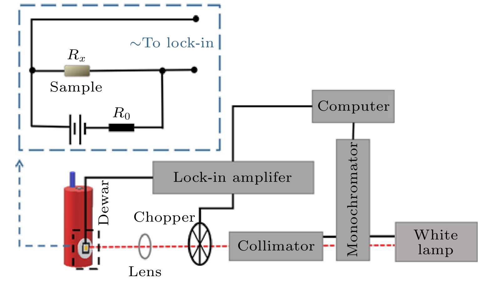
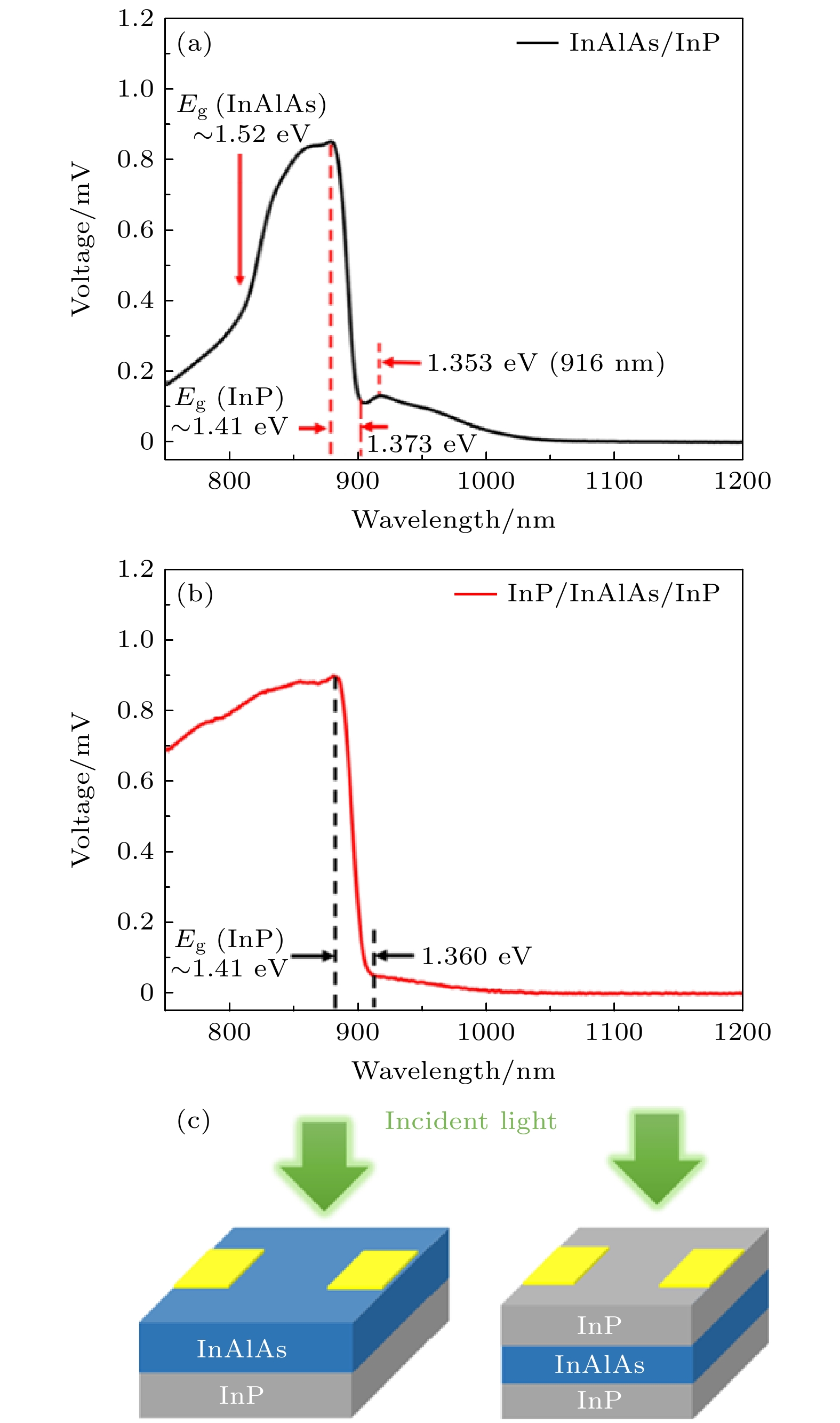
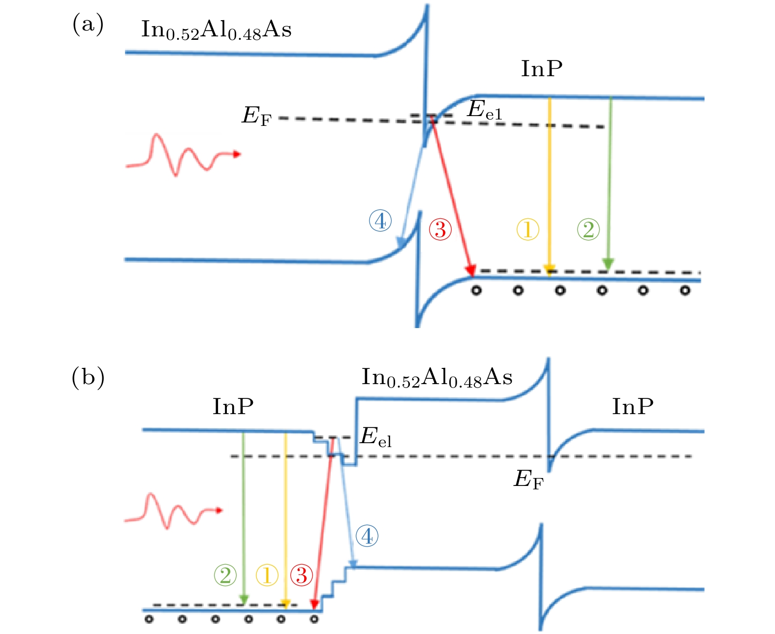
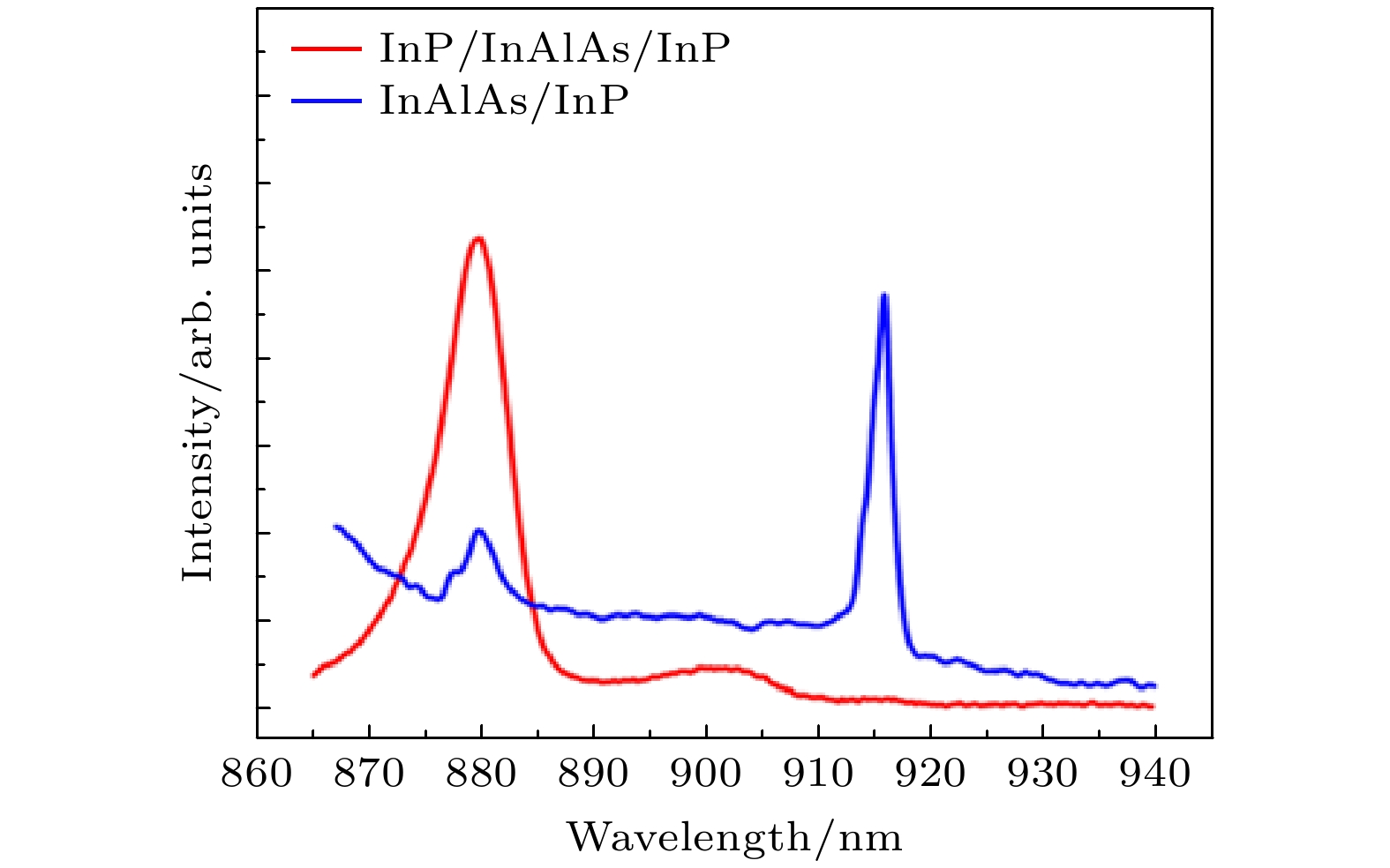
应用光电导谱(PC)和光致发光谱(PL)研究了由分子束外延在InP(100)衬底上生长In0.52Al0.48As获得的两种异质结外延结构, 分别是在InP衬底上生长InAlAs形成的正向异质结样品(样品A: In0.52Al0.48As/InP)和InAlAs层继续生长InP形成的上层为反向异质结的双异质结样品(样品B: InP/In0.52Al0.48As/InP). PL和PC实验采用光从表面入射激发的测量构型, 样品测量温度为77 K. 样品A的PC谱显示, 在激发光能量大于表面In0.52Al0.48As层的带隙时出现了电导陡降的反常变化, 还在916 nm波长处呈现一小的电导峰结构. PL谱对应此波长位置则出现很强的发光峰. 样品B则未观察到上述光谱特征, 该差异可从两类异质结不同的界面电子结构获得解释.Photoconductivity (PC) spectroscopy and photoluminescence (PL) spectroscopy were used to characterize two heterostructure configurations of InAlAs/InP grown by molecular beam epitaxy (MBE) on the InP (100) substrate. The sample A is the type called normal heterostructure, which has an In0.52Al0.48As layer grown on InP, while sample B is called the inverse type formed by an InP cap layer on In0.52Al0.48As. The front excitation was employed in both PC experiment and PL experiment and the measurements were conducted at 77 K. The PC spectrum of sample A shows an abnormal step-like drop when the photon energy is larger than the energy band gap of In0.52Al0.48As. The phenomenon implies that the conductance of sample is a multilayer effect including the contribution of interfacial two-dimensional electron gas (2DEG). Moreover, a conductance peak is observed at 916 nm below the bandgap of InP. Accordingly, an intense luminescent peak at the wavelength manifests in the PL spectrum. The origin of the 916 nm peak is attributed to the recombination of 2DEG electrons with the valence band holes excited near the interface. However, the spectral feature of the above energy does not exist in both PC and PL spectra of sample B. This difference may be explained by the different interface electronic structures of the inverse interface. For the latter case, considering that a graded variation in In-As-P composition is related to the inverse interface of InP/InAlAs, the band bending effect should be weak. In such a case, the bound energy of 2DEG in the interface potential well is raised closer to the conductance band of the bulk. Consequently, the recombination energy of 2DEG at the inverse interface with the holes in the valence band is close to the band-to-band transition of InP bulk and the luminescence is difficult to be distinguished from that of bulk InP. The work also demonstrates that the comparative study with both PC technique and PL technique is helpful to provide a full insight into the interface electronic property.
-
Keywords:
- semiconductor spectroscopy /
- semiconductor interface /
- photoconductance /
- photoluminescence
[1] Burstein L, Shapira Y, Bennett B R, Alamo J A D 1996 J. Appl. Phys 78 7163
 Google Scholar
[2] Holthoff E L, Heaps D A, Pellegrino P M 2010 IEEE Sens. J. 10 572
 Google Scholar
[3] Demir I, Elagoz S 2017 Superlattices Microstruct. 104 140
 Google Scholar
[4] Ramirez D A, Hayat M M, Karve G, Campbell J C, Teich M. C 2005 IEEE Leos Meeting Conference. IEEE Sydney NSW Australia, October 22–28, 2005 p387
[5] Hellara J, Hassen F, Maaref H, Souliere V, Monteil Y 2003 Physica E 17 229
 Google Scholar
[6] Yerino C D, Liang B, Huffaker D L, Simmonds P J, Lee M L, 2017 J. Vac. Sci. Technol., B 35 010801
 Google Scholar
[7] Hellara J, Hassen F, Maaref H, Souliere V, Monteil Y 2002 Mater Sci. Eng. , C 21 231
 Google Scholar
[8] Bohrer J, Krost A, Heitz R, Heinrichsdorff F, Eckey L, Bimberg D, Cerva H 1997 Appl. Phys. Lett. 68 1072
 Google Scholar
[9] Vignaud D, Wallart X, Mollot F, Sermage B 1998 J. Appl. Phys. 84 2138
 Google Scholar
[10] Vignaud D, Wallart X, Mollot F 1998 J. Appl. Phys. 76 2324
 Google Scholar
[11] Duez V, Vanbeìsien O, Lippens D, Vignaud D, Wallart X, Mollot F 1999 J. Appl. Phys. 85 2202
 Google Scholar
[12] Pocas L C, Duarte J L, Dias I F L, Laureto E, Lourenco S A, Filho, Toginho D O, Meneses E A, Mazzaro I, Harmand J C 2002 J. Appl. Phys. 91 8999
 Google Scholar
[13] Gocalinska A M, Mura E E, Manganaro M, Juska G, Pelucchi E 2020 Phys. Rev. B 101 165310
 Google Scholar
[14] Smiri B, Fraj I, Saidi F, Mghaieth R, Maaref H 2018 J. Alloys Compd. 736 29
 Google Scholar
[15] Esmaielpour H, Whiteside V R, Hirst L C, Tischler J G, Walters R J, Sellers I R 2017 J. Appl. Phys. 121 235301
 Google Scholar
[16] Smiri B, Fraj I, Saidi F, Mghaieth R, Maaref H 2019 Appl. Phys. A 125 134
 Google Scholar
[17] Smiri B, Fraj I, Saidi F, Mghaieth R, Maaref H 2020 J. Appl. Phys. 59 022001
 Google Scholar
[18] Madelung O 2004 Semiconductors: Data Handbook (1st Ed.) (New York: Springer-Heidelberg Press) p139
[19] Gong B, Zha F X, 2020 Rev. Sci. Instrum. 91 013105
 Google Scholar
[20] Hurd C M, McAlister S P, McKinnon W R, Stewart B R, Day D J, Mandeville P, SpringThorpe A J 1988 J. Appl. Phys. 63 4706
 Google Scholar
[21] Meng X, Tan C H, Dimler S, David J P R, Ng J S 2014 Opt. Express 22 22608
 Google Scholar
[22] Gilinsky A M, Dmitriev D V, Toropov A I, Zhuravlev K S 2017 Semicond. Sci. Technol. 32 095009
 Google Scholar
[23] Bergman J P, Lundstrom T, Monemar B, Amano H, Akasaki I 1996 Appl. Phys. Lett. 69 3456
 Google Scholar
-
-
[1] Burstein L, Shapira Y, Bennett B R, Alamo J A D 1996 J. Appl. Phys 78 7163
 Google Scholar
[2] Holthoff E L, Heaps D A, Pellegrino P M 2010 IEEE Sens. J. 10 572
 Google Scholar
[3] Demir I, Elagoz S 2017 Superlattices Microstruct. 104 140
 Google Scholar
[4] Ramirez D A, Hayat M M, Karve G, Campbell J C, Teich M. C 2005 IEEE Leos Meeting Conference. IEEE Sydney NSW Australia, October 22–28, 2005 p387
[5] Hellara J, Hassen F, Maaref H, Souliere V, Monteil Y 2003 Physica E 17 229
 Google Scholar
[6] Yerino C D, Liang B, Huffaker D L, Simmonds P J, Lee M L, 2017 J. Vac. Sci. Technol., B 35 010801
 Google Scholar
[7] Hellara J, Hassen F, Maaref H, Souliere V, Monteil Y 2002 Mater Sci. Eng. , C 21 231
 Google Scholar
[8] Bohrer J, Krost A, Heitz R, Heinrichsdorff F, Eckey L, Bimberg D, Cerva H 1997 Appl. Phys. Lett. 68 1072
 Google Scholar
[9] Vignaud D, Wallart X, Mollot F, Sermage B 1998 J. Appl. Phys. 84 2138
 Google Scholar
[10] Vignaud D, Wallart X, Mollot F 1998 J. Appl. Phys. 76 2324
 Google Scholar
[11] Duez V, Vanbeìsien O, Lippens D, Vignaud D, Wallart X, Mollot F 1999 J. Appl. Phys. 85 2202
 Google Scholar
[12] Pocas L C, Duarte J L, Dias I F L, Laureto E, Lourenco S A, Filho, Toginho D O, Meneses E A, Mazzaro I, Harmand J C 2002 J. Appl. Phys. 91 8999
 Google Scholar
[13] Gocalinska A M, Mura E E, Manganaro M, Juska G, Pelucchi E 2020 Phys. Rev. B 101 165310
 Google Scholar
[14] Smiri B, Fraj I, Saidi F, Mghaieth R, Maaref H 2018 J. Alloys Compd. 736 29
 Google Scholar
[15] Esmaielpour H, Whiteside V R, Hirst L C, Tischler J G, Walters R J, Sellers I R 2017 J. Appl. Phys. 121 235301
 Google Scholar
[16] Smiri B, Fraj I, Saidi F, Mghaieth R, Maaref H 2019 Appl. Phys. A 125 134
 Google Scholar
[17] Smiri B, Fraj I, Saidi F, Mghaieth R, Maaref H 2020 J. Appl. Phys. 59 022001
 Google Scholar
[18] Madelung O 2004 Semiconductors: Data Handbook (1st Ed.) (New York: Springer-Heidelberg Press) p139
[19] Gong B, Zha F X, 2020 Rev. Sci. Instrum. 91 013105
 Google Scholar
[20] Hurd C M, McAlister S P, McKinnon W R, Stewart B R, Day D J, Mandeville P, SpringThorpe A J 1988 J. Appl. Phys. 63 4706
 Google Scholar
[21] Meng X, Tan C H, Dimler S, David J P R, Ng J S 2014 Opt. Express 22 22608
 Google Scholar
[22] Gilinsky A M, Dmitriev D V, Toropov A I, Zhuravlev K S 2017 Semicond. Sci. Technol. 32 095009
 Google Scholar
[23] Bergman J P, Lundstrom T, Monemar B, Amano H, Akasaki I 1996 Appl. Phys. Lett. 69 3456
 Google Scholar
计量
- 文章访问数: 4812
- PDF下载量: 191
- 被引次数: 0


 下载:
下载:


