-
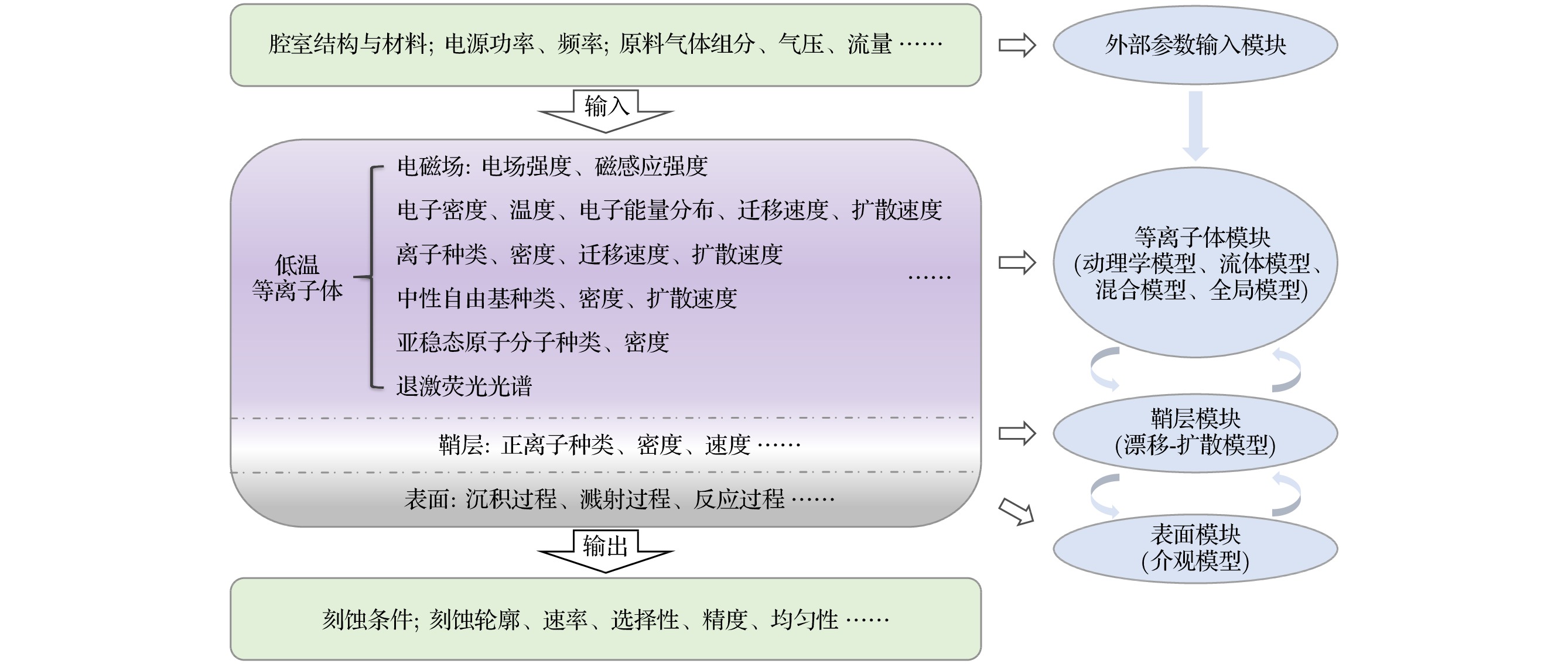
半导体芯片是信息时代的基石, 诸如大数据、机器学习、人工智能等新兴技术领域的快速发展离不开源自芯片层面的算力支撑. 在越来越高的算力需求驱动下, 芯片工艺不断追求更高的集成度与更小的器件体积. 作为芯片制造工序的关键环节, 刻蚀工艺因此面临巨大的挑战. 基于低温等离子体处理技术的干法刻蚀工艺是高精细电路图案刻蚀的首选方案, 借助等离子体仿真模拟, 人们已经能够在很大程度上缩小实验探索的范围, 在海量的参数中找到最优工艺条件. 电子碰撞截面是等离子体刻蚀模型的关键输入参数, 深刻影响着模型预测结果的可靠性. 本文主要介绍了低温等离子体建模的基本理论, 重点强调电子碰撞截面数据在数值模拟中的重要作用. 与此同时, 本文概述了获取刻蚀气体截面数据的理论与实验方法. 最后总结了刻蚀相关原子分子的电子碰撞截面研究现状, 并展望了未来的研究前景.Semiconductor chips are the cornerstone of the information age, which play a vital role in the rapid development of emerging technologies such as big data, machine learning, and artificial intelligence. Driven by the growing demand for computing power, the chip manufacturing industry has been committed to pursuing higher level of integration and smaller device volumes. As a critical step in the chip manufacturing processes, the etching process therefore faces great challenges. Dry etching (or plasma etching) process based on the low-temperature plasma science and technology is the preferred solution for etching the high-precision circuit pattern. In the low-temperature plasma, electrons obtain energy from the external electromagnetic field and transfer the energy to other particles through collision process. After a series of complex physical and chemical reactions, a large number of active particles such as electrons, ions, atoms and molecules in excited states, and radicals are finally generated, providing the material conditions for etching the substrate. Dry etching chamber is a nonlinear system with multiple space-time dimensions, multiple reaction levels and high complexity. Facing such a complex system, only by fully understanding the basic physical and chemical reaction of the etching process can we optimize the process parameters and improve the etching conditions, so as to achieve precision machining of the semiconductor and meet the growing demand of the chip industry for etching rate and yield. In the early days, the process conditions of dry etching were determined through the trial-and-error method, which is characterized by high cost and low yield. However, with the help of plasma simulation, nowadays people have been able to narrow the scope of experiment to a large extent, and find out efficiently the optimal process conditions in a large number of parameters. In this review, we first introduce the basic theory of the mostly used models for plasma simulation including kinetic, fluid dynamic, hybrid and global models, in which the electron collision cross sections are the key input parameters. Since the formation of the low-temperature plasma is driven by the electron-heavy particle collision processes, and the active species for plasma etching are generated in the reactions induced by electron impact, the accuracy and completeness of the cross-section data greatly affect the reliability of the simulation results. Then, the theoretical and experimental methods of obtaining the cross-section data of etching gases are summarized. Finally, the research status of the electron collision cross sections of etching atoms and molecules is summarized, and the future research prospect is discussed.
[1] 张汝京 等 2017 纳米集成电路制造工艺(第二版) (北京: 清华大学出版社)
Zhang R J, et al. 2017 Nanoscale Integrated Circuits — The Manufacturing Process (2nd Ed.) (Beijing: Tsinghua University Press
[2] 张海洋 等 2018 等离子体蚀刻及其在大规模集成电路制造中的应用 (北京: 清华大学出版社)
Zhang H Y, et al. 2018 Plasma Etching and its Application in Large Scale Integrated Circuit Manufacturing (Beijing: Tsinghua University Press
[3] Oehrlein G S 1986 Phys. Today 39 26
 Google Scholar
[4] Manos D M, Flamm D L 1989 Plasma Etching: An Introduction (San Diego: Academic Press
[5] Moore G E 1965 Electronics 38 114
 Google Scholar
[6] Bondur J A 1976 J. Vac. Sci. Technol. 13 1023
 Google Scholar
[7] Jansen H, Gardeniers H, de Boer M, Elwenspoek M, Fluitman J 1996 J. Micromech. Microeng. 6 14
 Google Scholar
[8] Posseme N 2017 Plasma Etching Processes for CMOS Devices Realization (London: ISTE Press
[9] Kambara M, Kawaguchi S, Lee H J, Ikuse K, Hamaguchi S, Ohmori T, Ishikawa K 2023 Jpn. J. Appl. Phys. 62 SA0803
 Google Scholar
[10] Capps N E, Mackie N M, Fisher E R 1998 J. Appl. Phys. 84 4736
 Google Scholar
[11] Cardinaud C 2018 C. R. Chim. 21 723
 Google Scholar
[12] Efremov A, Lee B J, Kwon K H 2021 Materials 14 1432
 Google Scholar
[13] Wang D H, Wang S X, Nie Z W, Wang L H, Xu Y C, Du X J, Zhu L F 2022 Plasma Sources Sci. Technol. 31 045012
 Google Scholar
[14] Capitelli M, Bardsley J N 1990 Nonequilibrium Processes in Partially Ionized Gases (New York: Plenum Press) pp283–290
[15] National Research Council 1996 Database Needs for Modeling and Simulation of Plasma Processing (Washington, D.C.: National Academies Press
[16] Huo W M, Kim Y K 1999 IEEE Trans. Plasma Sci. 27 1225
 Google Scholar
[17] Kline L E, Kushner M J 1989 Crit. Rev. Solid State Mater. Sci. 16 1
 Google Scholar
[18] Sommerer T J, Kushner M J 1992 J. Appl. Phys. 71 1654
 Google Scholar
[19] Lymberopoulos D P, Economou D J 1995 J. Res. Nat. Inst. Stand. Technol. 100 473
 Google Scholar
[20] Li M, Wu H M, Chen Y 1995 IEEE Trans. Plasma Sci. 23 558
 Google Scholar
[21] Kushner M J, Collison W Z, Grapperhaus M J, Holland J P, Barnes M S 1996 J. Appl. Phys. 80 1337
 Google Scholar
[22] Wu H M, Yu B W, Li M, Yang Y 1997 IEEE Trans. Plasma Sci. 25 1
 Google Scholar
[23] Tago K, Kazumi H, Kobayashi K 1998 J. Alloys Compd. 279 60
 Google Scholar
[24] Morgan W L 2000 Adv. At. Mol. Opt. Phys. 43 79
 Google Scholar
[25] Mason N J 2009 J. Phys. D: Appl. Phys. 42 194003
 Google Scholar
[26] Bartschat K, Kushner M J 2016 Proc. Natl. Acad. Sci. U. S. A. 113 7026
 Google Scholar
[27] Carbone E, Graef W, Hagelaar G, Boer D, Hopkins M M, Stephens J C, Yee B T, Pancheshnyi S, van Dijk J, Pitchford L 2021 Atoms 9 16
 Google Scholar
[28] Sakai Y 2002 Appl. Surf. Sci. 192 327
 Google Scholar
[29] Morgan W L 1992 Plasma Chem. Plasma Process. 12 449
 Google Scholar
[30] Morgan W L 1992 Plasma Chem. Plasma Process. 12 477
 Google Scholar
[31] Christophorou L G, Olthoff J K 2001 Adv. At. Mol. Opt. Phys. 44 59
 Google Scholar
[32] Christophorou L G, Olthoff J K 2002 Appl. Surf. Sci. 192 309
 Google Scholar
[33] Pitchford L C, Alves L L, Bartschat K, Biagi S F, Bordage M C, Phelps A V, Ferreira C M, Hagelaar G J M, Morgan W L, Pancheshnyi S, Puech V, Stauffer A, Zatsarinny O 2013 J. Phys. D: Appl. Phys. 46 334001
 Google Scholar
[34] Alves L L, Bartschat K, Biagi S F, Bordage M C, Pitchford L C, Ferreira C M, Hagelaar G J M, Morgan W L, Pancheshnyi S, Phelps A V, Puech V, Zatsarinny O 2013 J. Phys. D: Appl. Phys. 46 334002
 Google Scholar
[35] Bordage M C, Biagi S F, Alves L L, Bartschat K, Chowdhury S, Pitchford L C, Hagelaar G J M, Morgan W L, Puech V, Zatsarinny O 2013 J. Phys. D: Appl. Phys. 46 334003
 Google Scholar
[36] Kawaguchi S, Satoh K, Itoh H 2015 Jpn. J. Appl. Phys. 54 01AC01
 Google Scholar
[37] Alves L L, Coche P, Ridenti M A, Guerra V 2016 Eur. Phys. J. D 70 124
 Google Scholar
[38] Bartschat K, Tennyson J, Zatsarinny O 2017 Plasma Processes Polym. 14 1600093
 Google Scholar
[39] Xu Y C, Du X J, Li T J, Wang L H, Ma Z R, Zhu L F 2020 Plasma Sources Sci. Technol. 29 085005
 Google Scholar
[40] Gupta D 2020 Appl. Sci. Converg. Technol. 29 125
 Google Scholar
[41] Sun Q, Wang S X, Xu Y C, Ma K, Wang L H, Li T J, Zhu L F 2022 J. Electron Spectrosc. Relat. Phenom. 258 147218
 Google Scholar
[42] Colonna G, D’Angola A 2022 Plasma Modeling Methods and Applications (2nd Ed.) (London: IOP Publishing
[43] Alves L L, Bogaerts A, Guerra V, Turner M M 2018 Plasma Sources Sci. Technol. 27 023002
 Google Scholar
[44] Hurlbatt A, Gibson A R, Schröter S, Bredin J, Foote A P S, Grondein P, O’Connell D, Gans T 2017 Plasma Processes Polym. 14 1600138
 Google Scholar
[45] Hagelaar G J M, Pitchford L C 2005 Plasma Sources Sci. Technol. 14 722
 Google Scholar
[46] Petrović Z Lj, Dujko S, Marić D, Malović G, Nikitović Ž, Šašić O, Jovanović J, Stojanović V, Radmilović-Radenović M 2009 J. Phys. D: Appl. Phys. 42 194002
 Google Scholar
[47] Surendra M, Graves D B, Jellum G M 1990 Phys. Rev. A 41 1112
 Google Scholar
[48] Janssen J F J, Pitchford L C, Hagelaar G J M, van Dijk J 2016 Plasma Sources Sci. Technol. 25 055026
 Google Scholar
[49] Kolobov V I, Arslanbekov R R 2006 IEEE Trans. Plasma Sci. 34 895
 Google Scholar
[50] Kolobov V I, Arslanbekov R R 2012 J. Comput. Phys. 231 839
 Google Scholar
[51] Arslanbekov R R, Kolobov V I, Frolova A A 2013 Phys. Rev. E 88 063301
 Google Scholar
[52] Birdsall C K 1991 IEEE Trans. Plasma Sci. 19 65
 Google Scholar
[53] Vahedi V, Surendra M 1995 Comput. Phys. Commun. 87 179
 Google Scholar
[54] Longo S 2000 Plasma Sources Sci. Technol. 9 468
 Google Scholar
[55] Nanbu K 2000 IEEE Trans. Plasma Sci. 28 971
 Google Scholar
[56] Toneli D A, Pessoa R S, Roberto M, Gudmundsson J T 2019 Plasma Sources Sci. Technol. 28 025007
 Google Scholar
[57] Kushner M J 2009 J. Phys. D: Appl. Phys. 42 194013
 Google Scholar
[58] LXCat: Plasma Data Exchange Project Database (http:// fr.lxcat.net/home/) [2023-10-5]
[59] Tejero-del-Caz A, Guerra V, Gonçalves D, Lino da Silva M, Marques L, Pinhão N, Pintassilgo C D, Alves L L 2019 Plasma Sources Sci. Technol. 28 043001
 Google Scholar
[60] COMSOL MULTIPHYSICS (http://cn.comsol.com/) [2023-10-5]
[61] Chutjian A, Garscaddenb A, Wadehra J M 1996 Phys. Rep. 264 393
 Google Scholar
[62] Fabrikant I I, Eden S, Mason N J, Fedor J 2017 Adv. At. Mol. Opt. Phys. 66 545
 Google Scholar
[63] Pshenichnyuk S A, Asfandiarov N L, Vorob’ev A S, Matejčík Š 2022 Phys. Usp. 65 163
 Google Scholar
[64] Underwood-Lemons T, Gergel T J, Moore J H 1995 J. Chem. Phys. 102 119
 Google Scholar
[65] Christophorou L G, Olthoff J K 2001 Int. J. Mass Spectrom. 205 27
 Google Scholar
[66] Fedor J, May O, Allan M 2008 Phys. Rev. A 78 032701
 Google Scholar
[67] Bose D, Rao M, Govindan T R, Meyyappan M 2003 Plasma Sources Sci. Technol. 12 225
 Google Scholar
[68] Zatsarinny O, Bartschat K 2013 J. Phys. B: At. Mol. Opt. Phys. 46 112001
 Google Scholar
[69] Takatsuka K, McKoy V 1981 Phys. Rev. A 24 2473
 Google Scholar
[70] Schneider B I, Rescigno T N 1988 Phys. Rev. A 37 3749
 Google Scholar
[71] Zammit M C, Fursa D V, Savage J S, Bray I 2017 J. Phys. B: At. Mol. Opt. Phys. 50 123001
 Google Scholar
[72] Antony B K, Joshipura K N, Mason N J 2005 J. Phys. B: At. Mol. Opt. Phys. 38 189
 Google Scholar
[73] Kim Y K 2001 Phys. Rev. A 64 032713
 Google Scholar
[74] Kim Y K, Rudd M E 1994 Phys. Rev. A 50 3954
 Google Scholar
[75] Tanaka H, Brunger M J, Campbell L, Kato H, Hoshino M, Rau A R P 2016 Rev. Mod. Phys. 88 025004
 Google Scholar
[76] Bartschat K 2013 J. Phys. D: Appl. Phys. 46 334004
 Google Scholar
[77] de Urquijo J, Arriaga C A, Cisneros C, Alvarez I 1999 J. Phys. D: Appl. Phys. 32 41
 Google Scholar
[78] Liu X J, Zhu L F, Jiang X M, Yuan Z S, Cai B, Chen X J, Xu K Z 2001 Rev. Sci. Instrum. 72 3357
 Google Scholar
[79] Fuss M C, Sanz A G, Blanco F, Oller J C, Limão-Vieira P, Brunger M J, García G 2013 Phys. Rev. A 88 042702
 Google Scholar
[80] Lozano A I, Oller J C, Krupa K, Ferreira da Silva F, Limão-Vieira P, Blanco F, Muñoz A, Colmenares R, García G 2018 Rev. Sci. Instrum. 89 063105
 Google Scholar
[81] Traoré Dubuis A, Costa F, Ferreira da Silva F, Limão-Vieira P, Oller J C, Blanco F, García G 2018 Chem. Phys. Lett. 699 182
 Google Scholar
[82] Costa F, Álvarez L, Lozano A I, Blanco F, Oller J C, Muñoz A, Souza Barbosa A, Bettega M H F, Ferreira da Silva F, Limão-Vieira P, White R D, Brunger M J, García G 2019 J. Chem. Phys. 151 084310
 Google Scholar
[83] Sullivan J P, Gilbert S J, Marler J P, Greaves R G, Buckman S J, Surko C M 2002 Phys. Rev. A 66 042708
 Google Scholar
[84] Mann A, Linder F 1992 J. Phys. B: At. Mol. Opt. Phys. 25 533
 Google Scholar
[85] Boesten L, Tanaka H, Kobayashi H, Dillon M A, Kimura M 1992 J. Phys. B: At. Mol. Opt. Phys. 25 1607
 Google Scholar
[86] Gauf A, Navarro C, Balch G, Hargreaves L R, Khakoo A, Winstead C, McKoy V 2013 Phys. Rev. A 87 012710
 Google Scholar
[87] Read F H, Channing J M 1996 Rev. Sci. Instrum. 67 2372
 Google Scholar
[88] Allan M 2004 Phys. Scr. 2004 161
 Google Scholar
[89] Gote M, Ehrhardt H 1995 J. Phys. B: At. Mol. Opt. Phys. 28 3957
 Google Scholar
[90] Mann A, Linder F 1992 J. Phys. B: At. Mol. Opt. Phys. 25 545
 Google Scholar
[91] Inokuti M 1971 Rev. Mod. Phys. 43 297
 Google Scholar
[92] Kim Y K 2007 J. Chem. Phys. 126 064305
 Google Scholar
[93] Wang S X, Zhu L F 2022 Chin. Phys. B 31 083401
 Google Scholar
[94] Zhong Z P, Feng R F, Xu K Z, Wu S L, Zhu L F, Zhang X J, Ji Q, Shi Q C 1997 Phys. Rev. A 55 1799
 Google Scholar
[95] Lassettre E N, Skerbele A 1971 J. Chem. Phys. 54 1597
 Google Scholar
[96] Zobel J, Mayer U, Jung K, Ehrhardt H 1996 J. Phys. B: At. Mol. Opt. Phys. 29 813
 Google Scholar
[97] Zetner P W, Kanik I, Trajmar S 1998 J. Phys. B: At. Mol. Opt. Phys. 31 2395
 Google Scholar
[98] Kato H, Kawahara H, Hoshino M, Tanaka H, Brunger M J, Kim Y K 2007 J. Chem. Phys. 126 064307
 Google Scholar
[99] Li H H, Wang S X, Zhu J H, Nie Z W, Chen J F, Wang L H, Ma W L, Zhu L F 2023 Plasma Sources Sci. Technol. 32 065011
 Google Scholar
[100] Goto M, Nakamura K, Toyoda H, Sugai H 1994 Jpn. J. Appl. Phys. 33 3602
 Google Scholar
[101] Sugai H, Toyoda H, Nakano T, Goto M 1995 Contrib. Plasma Phys. 35 415
 Google Scholar
[102] Morgan W L, Winstead C, McKoy V 2001 J. Appl. Phys. 90 2009
 Google Scholar
[103] Schülke W 2007 Electron Dynamics by Inelastic X-ray Scattering (Oxford: Oxford University Press
[104] Xie B P, Zhu L F, Yang K, Zhou B, Hiraoka N, Cai Y Q, Yao Y, Wu C Q, Wang E L, Feng D L 2010 Phys. Rev. A 82 032501
 Google Scholar
[105] Zhu L F, Wang L S, Xie B P, Yang K, Hiraoka N, Cai Y Q, Feng D L 2011 J. Phys. B: At. Mol. Opt. Phys. 44 025203
 Google Scholar
[106] Mochizuki Y, Murai H, Kato H, Hoshino M, Tanaka H 2015 J. Phys. Conf. Ser. 635 052048
 Google Scholar
[107] Khakoo M A, Vandeventer P, Childers J G, Kanik I, Fontes C J, Bartschat K, Zeman V, Madison D H, Saxena S, Srivastava R, Stauffer A D 2004 J. Phys. B: At. Mol. Opt. Phys. 37 247
 Google Scholar
[108] Filipović D M, Marinković B P, Pejčev V, Vušković L 2000 J. Phys. B: At. Mol. Opt. Phys. 33 2081
 Google Scholar
[109] Filipović D M, Marinković B P, Pejčev V, Vušković L 2000 J. Phys. B: At. Mol. Opt. Phys. 33 677
 Google Scholar
[110] Chutjian A, Cartwright D C 1981 Phys. Rev. A 23 2178
 Google Scholar
[111] Bull J N, Bart M, Vallance C, Harland P W 2013 Phys. Rev. A 88 062710
 Google Scholar
[112] Karwasz G P, Możejko P, Song M Y 2014 Int. J. Mass Spectrom. 365–366 232
 Google Scholar
[113] Makochekanwa C, Oguri K, Suzuki R, Ishihara T, Hoshino M, Kimura M, Tanaka H 2006 Phys. Rev. A 74 042704
 Google Scholar
[114] Motlagh S, Moore J H 1998 J. Chem. Phys. 109 432
 Google Scholar
[115] Winters H F 1975 J. Chem. Phys. 63 3462
 Google Scholar
[116] Winters H F, Inokuti M 1982 Phys. Rev. A 25 1420
 Google Scholar
[117] Flaherty D W, Kasper M A, Baio J E, Graves D B, Winters H F, Winstead C, McKoy V 2006 J. Phys. D: Appl. Phys. 39 4393
 Google Scholar
[118] Ullrich J, Moshammer R, Dorn A, Dörner R, Schmidt L P H, Schmidt-Böcking H 2003 Rep. Prog. Phys. 66 1463
 Google Scholar
[119] Eppink A T J B, Parker D H 1997 Rev. Sci. Instrum. 68 3477
 Google Scholar
[120] Zhao Y R, Chen J J, Luo Z J, Chang Y, Yang J Y, Zhang W Q, Wu G R, Crane S W, Hansen C S, Ding H B, An F, Hu X X, Xie D Q, Ashfold M N R, Yuan K J, Yang X M 2023 Chem. Sci. 14 2501
 Google Scholar
[121] Adamovich I, Agarwal S, Ahedo E, Alves L L, Baalrud S, Babaeva N, Bogaerts A, Bourdon A, Bruggeman P J, Canal C, Choi E H, Coulombe S, Donkó Z, Graves D B, Hamaguchi S, Hegemann D, Hori M, Kim H H, Kroesen G M W, Kushner M J, Laricchiuta A, Li X, Magin T E, Mededovic Thagard S, Miller V, Murphy A B, Oehrlein G S, Puac N, Sankaran R M, Samukawa S, Shiratani M, Šimek M, Tarasenko N, Terashima K, Thomas Jr E, Trieschmann J, Tsikata S, Turner M M, van der Walt I J, van de Sanden M C M, von Woedtke T 2022 J. Phys. D: Appl. Phys. 55 373001
 Google Scholar
-
图 2 (a)以CHF3为原料气体的ICP刻蚀腔室(作图参考了文献[12]), 匹配器用于匹配电源输出阻抗与等离子体阻抗, 红色与蓝色线条分别代表磁场与电场, 鞘层区域的偏压可以将离子加速到几百eV, 高能离子垂直轰击表面导致各向异性刻蚀. 使用两个射频源, 可实现离子密度与能量的去耦合: 上方电源通过电感耦合供能, 可以控制离子密度; 下方电源通过电容耦合调节鞘层偏压, 可以控制离子的轰击能量; (b) 表面刻蚀部分, CmFn聚合物的钝化效应有助于各向异性刻蚀; (c) 等离子体内部及晶圆表面发生的主要物理化学过程
Fig. 2. (a) ICP etching chamber with CHF3 as feed gas (this picture was made with reference to Ref. [12]), the matching device is used to match the output impedance of the power supply and the plasma impedance, the red and blue lines represent the magnetic and electric fields respectively, the bias voltage in the sheath region can accelerate the ions to several hundred eV, and the high energy ions can vertically bombard the surface, leading to anisotropic etching. Using two RF sources, the decoupling of the ion density and energy can be achieved: the upper power supply can control the ion density through inductive coupling; the lower power supply can control the ion bombardment energy by adjusting the sheath bias through capacitive coupling. (b) The surface etching part, the passivation effect of CmFn polymer contributes to anisotropic etching. (c) The main physical and chemical processes that occur inside the plasma and on the wafer surface.
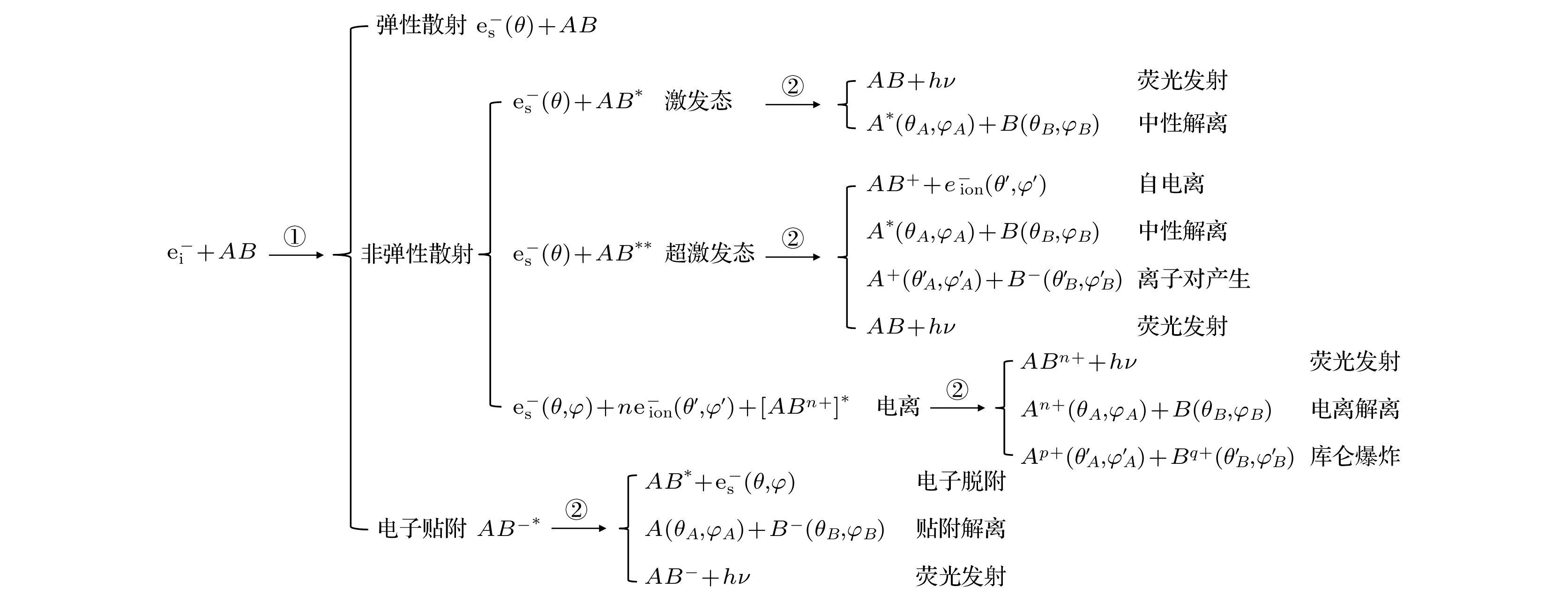
图 5 电子与双原子分子AB相互作用的初级过程①与次级过程②, 原子或多原子分子的情况是类似的. 注意到②中产生的处于激发态的原子分子或离子还会进一步演化
Fig. 5. Primary process ① and secondary process ② of electron interaction with diatomic molecule AB, and the interaction processes for atoms or polyatomic molecules are similar. Note that the excited atoms, molecules, and ions produced in ② will evolve further.
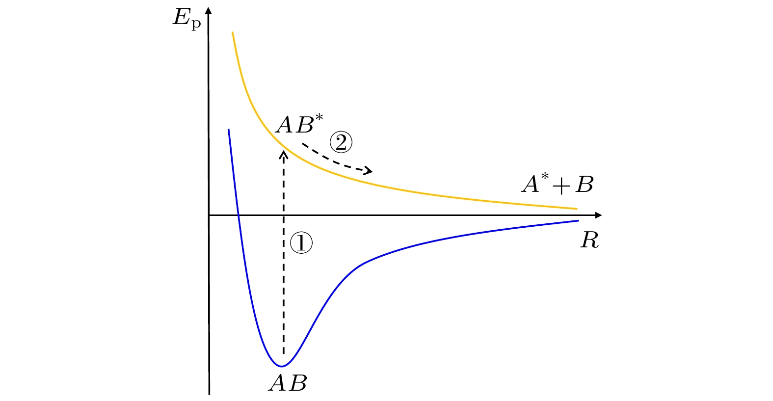
图 6 双原子分子AB的电子碰撞中性解离的两步过程示意图. 处于基态的分子AB首先被激发到解离态AB*, 随后沿着激发态势能曲线解离生成A*+B. 图示表明了次级过程的演化与初级过程无关, 只与原子分子所处激发态的性质(势能曲线)有关
Fig. 6. Schematic diagram of the two-step processes of electron-impact neutral dissociation of diatomic molecule AB. AB in the ground state is first excited to the dissociative state AB*, and then dissociates along the potential curve to form A*+B. The diagram indicates that the evolution of the secondary process is independent of the primary process, which is only related to the properties of the corresponding excited states (e. g. the potential curve).
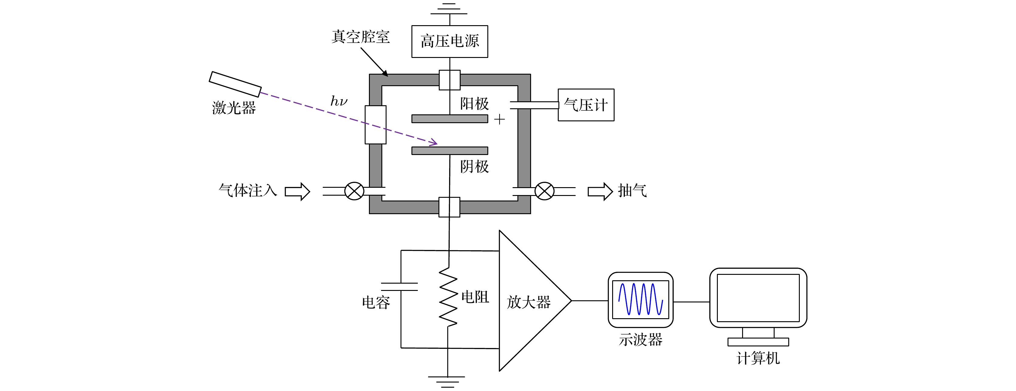
图 7 电子群实验(脉冲汤森装置)示意图[46,77]. 被激光照射后, 阴极放出的电子在电场作用下向阳极漂移, 与背景气体碰撞发生贴附、激发、电离等过程. 产生的电流(包括电子电流和离子电流)由探测电路监控, 背景气体的气压则由气压计检测
Fig. 7. Schematic diagram of swarm experiment (pulsed Townsend apparatus)[46,77]. The electrons released by photoemission drift towards the anode under the electric field, and the collision with the background gas leads to attachment, excitation, ionization, etc. The generated currents (including electronic current and ion current) are monitored by the detection circuit, and the pressure of the background gas is detected by the manometer.
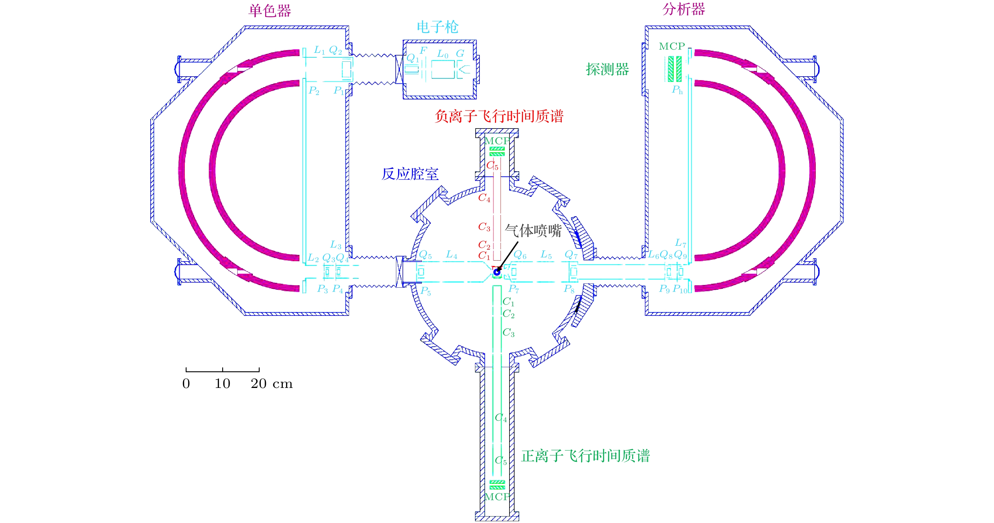
图 8 典型的电子束散射实验装置: 高分辨快电子能量损失谱仪[78]. 由电子枪发出的电子被静电半球单色器单色后在反应腔室中与样品气体碰撞(交叉束布局), 散射电子经过静电半球能量分析器后被位置灵敏探测器探测. 转动分析器可改变测量的散射角. 透镜(F, L)、偏转板(Q)、膜孔(P)等电子光学器件用于电子束的聚焦、准直、加(减)速与监测. 图中还展示了用于测量正、负离子的飞行时间质谱
Fig. 8. A typical apparatus for electron beam scattering experiment: high-resolution fast electron energy loss spectrometer[78]. The electrons emitted by the electron gun are monochromized by the electrostatic hemispherical monochromator and then collide with the sample gas in the reaction chamber (cross-beam layout), and the scattered electrons are detected by a position sensitive detector after passing through the electrostatic hemispherical energy analyzer. The measured scattering angle can be varied by rotating the analyzer. Electron optics such as lens (F, L), deflection plate (Q), and aperture (P) are used for focusing, collimating, acceleration (deceleration) and monitoring of the electron beam. Time-of-flight mass spectrometers used to measure positive and negative ions are also shown.
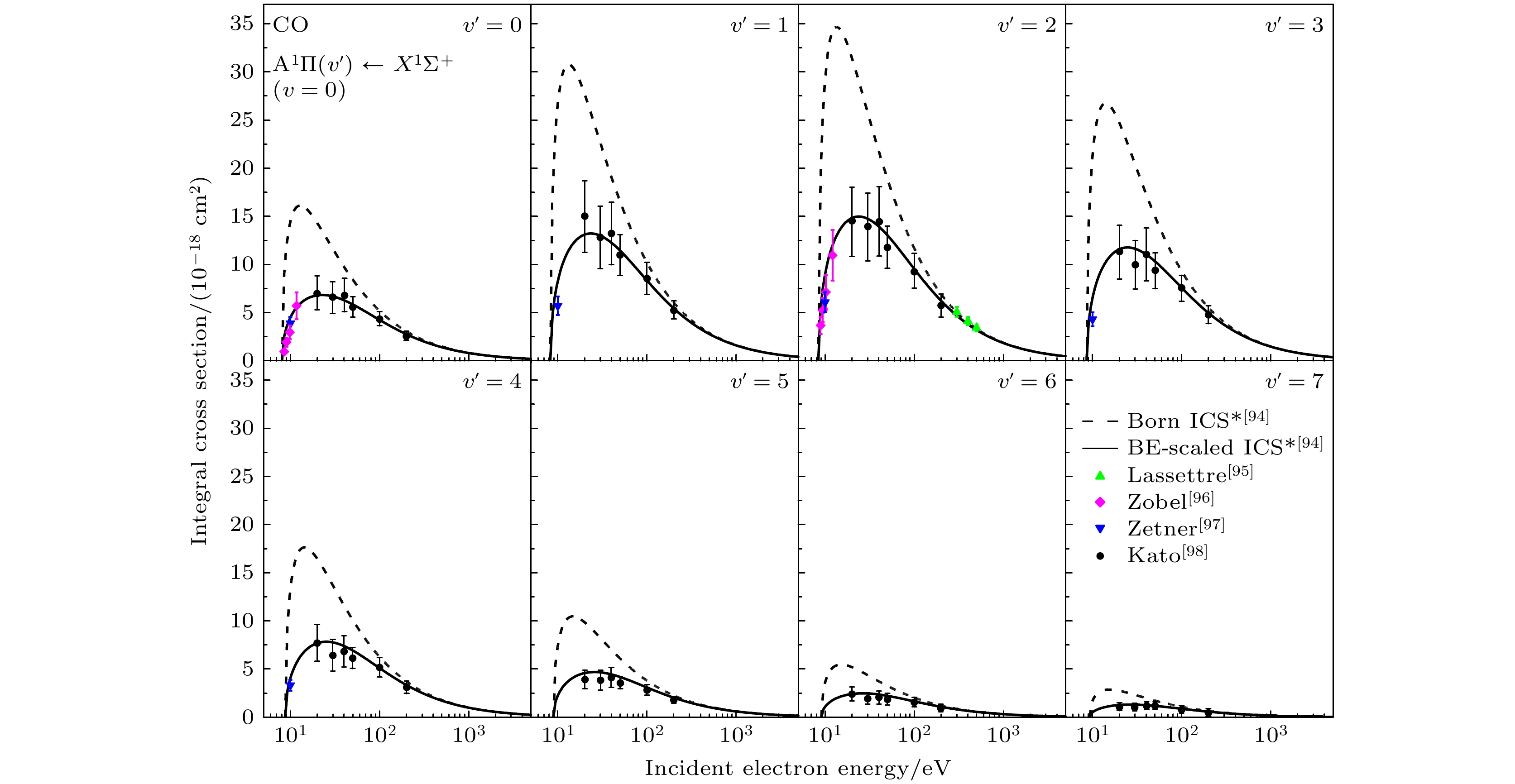
图 9 CO分子A1Π电子激发态不同振动能级的积分截面. *由文献[94]中测量的GOS计算得到. 可以看到, 虽然Born积分截面(虚线)在低能区比积分0°—180°微分散射截面得到的实验值(点)[95–98]大很多, 但是BE-scaled积分截面(实线)与实验值符合得很好
Fig. 9. Integral cross sections of the vibrational states of A1Π in carbon monoxide. * calculated from the GOSs reported in Ref. [94]. It can be seen that although the Born cross sections (dashed line) at the low energy region are much larger than the experimental values obtained by integrating the differential cross sections in the region of 0°–180° (dots)[95–98], the BE-scaled integral cross sections (solid line) agree very well with the experimental values.
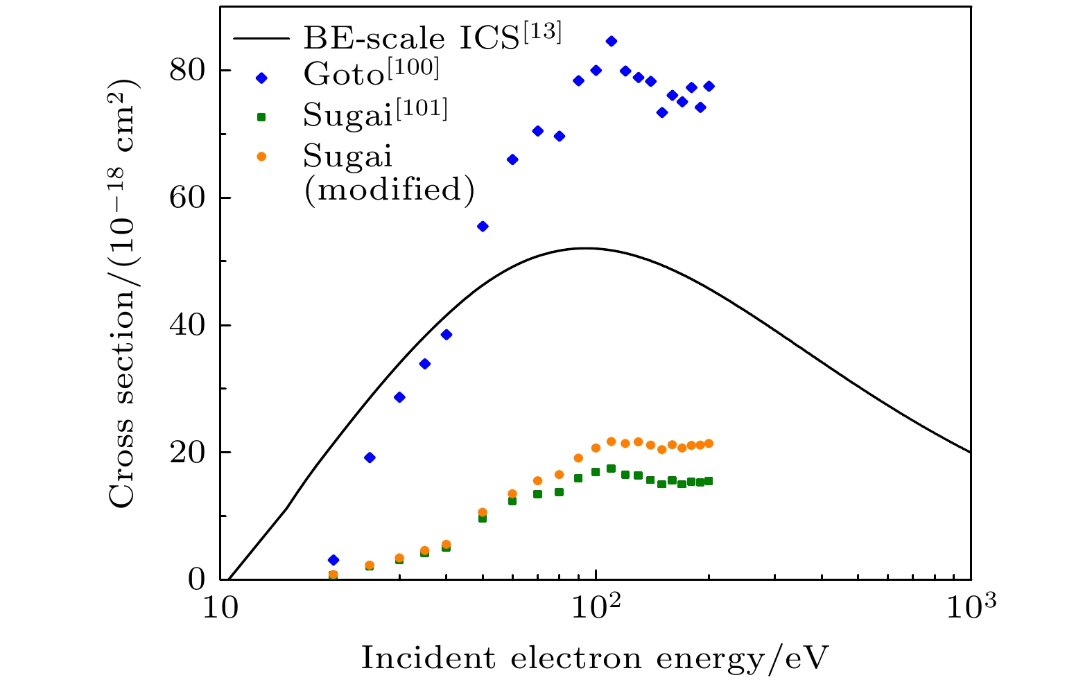
图 10 CHF3总中性解离截面的测量结果[13]. Sugai 等[101] 重新标定了他们之前的测量结果[100], 由于测量仅考虑了中性碎片CFx (x = 1—3), 加入了解离到CHF2和CHF的贡献进行修正
Fig. 10. Measured total dissociation cross sections into neutral species for CHF3[13]. Sugai et al.[101] recalibrated their previous experimental results[100]. Since their measurement only considered neutral fragments CFx (x = 1–3), the contributions of dissociation to CHF2 and CHF were added for correction.
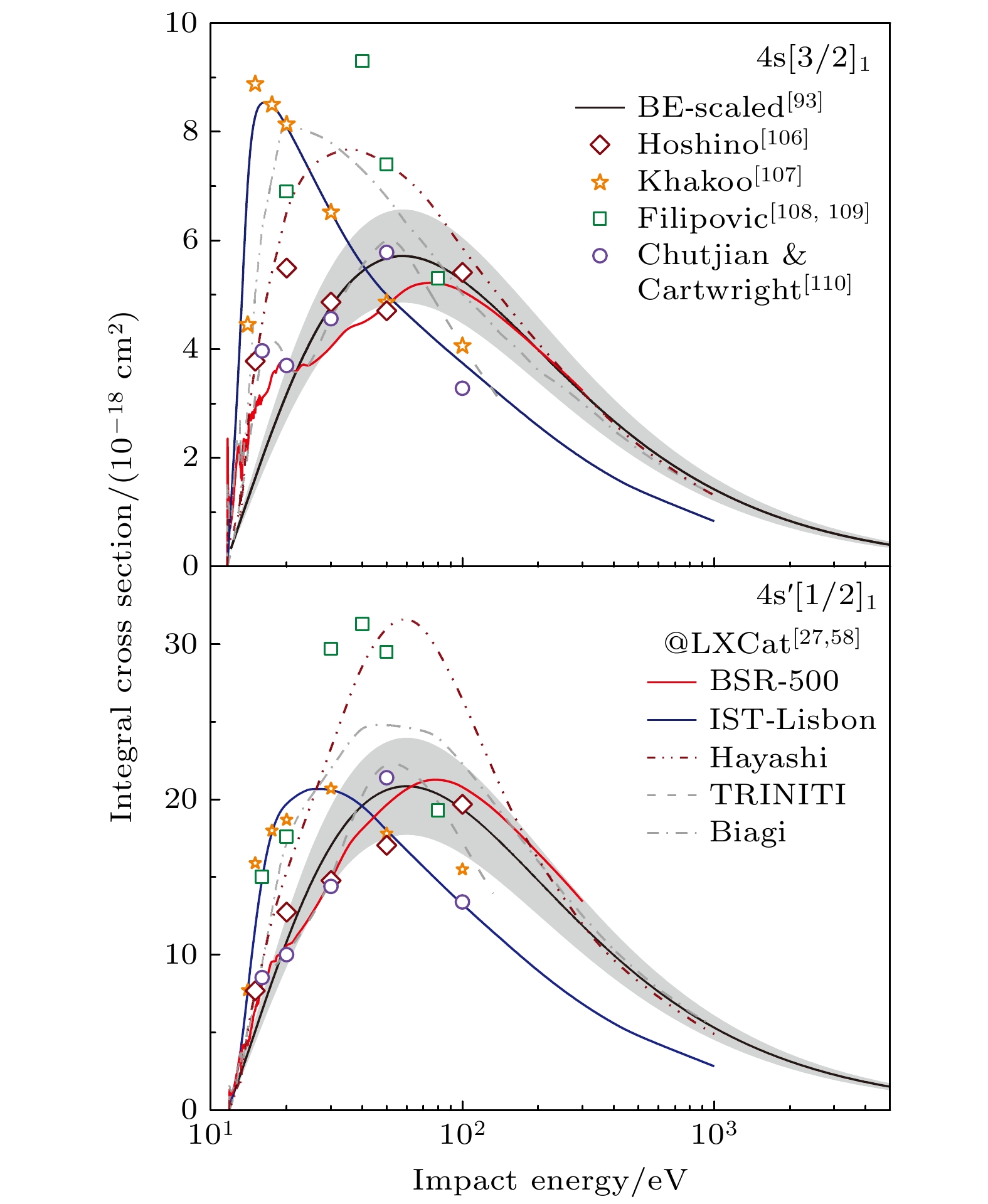
图 11 Ar原子4s[3/2]1, 4s′[1/2]1激发态的积分截面[93]. 数据点是低(中)能电子碰撞的实验结果[106–110]. 阴影区代表了BE-scaled积分截面(黑色实线)15%的实验误差[93], 其他曲线来自LXCat数据库[27,58]
Fig. 11. Integral cross sections for the 4s[3/2]1 and 4s′[1/2]1 states of Ar[93]. Dots are the experimental results measured by low (medium) energy electron impact[106–110]. The shaded areas indicate an experimental uncertainty of 15% of the BE-scaled integral cross sections (black solid lines)[93]. The other lines are the data from the LXCat database[27,58].
表 1 常用刻蚀气体. 等离子体刻蚀建模涉及的对象包含表格中的刻蚀气体本身、相应的解离碎片以及处于亚稳态的原子分子.
Table 1. Commonly used etching gases. The objects involved in plasma etching modeling include the etching gases in the table, the corresponding dissociation fragments, and the atoms and molecules in metastable states.
刻蚀气体 举例 氟碳化合物 CF4, CHF3, CH2F2, CH3F, C2F6,
C3F8, C4F8, C4F6······含氟分子 NF3, SF6, SiF4, CCl2F2······ 含氯与含溴分子 HBr, Cl2, BCl3······ 含氢分子 H2, CH4······ 附加气体 O2, N2, Ar, He······ 表 2 等离子体刻蚀建模所需的电子碰撞截面类型. 表格中的截面描述了低温等离子体中主要的电子碰撞过程
Table 2. Types of electron collision cross sections required for plasma etching modeling. The cross sections in the table describe the main electron collision processes in low temperature plasma.
建模所需截面类型 备注 总截面 与电子输运系数相关 弹性/动量转移截面 与电子输运系数相关 转动/振动激发截面 转动激发能量低, 可包含在弹性
截面中; 振动亚稳态可以是
多步解离(电离)的中间态电子态激发截面 刻蚀分子的电子激发态常常是解离态 解离截面 解离产物具有刻蚀活性 电离截面 电子、正离子产生过程 电子贴附截面 电子损失过程、负离子产生过程 中性解离/电离解离/
贴附解离截面解离为中性/正离子/负离子碎片 -
[1] 张汝京 等 2017 纳米集成电路制造工艺(第二版) (北京: 清华大学出版社)
Zhang R J, et al. 2017 Nanoscale Integrated Circuits — The Manufacturing Process (2nd Ed.) (Beijing: Tsinghua University Press
[2] 张海洋 等 2018 等离子体蚀刻及其在大规模集成电路制造中的应用 (北京: 清华大学出版社)
Zhang H Y, et al. 2018 Plasma Etching and its Application in Large Scale Integrated Circuit Manufacturing (Beijing: Tsinghua University Press
[3] Oehrlein G S 1986 Phys. Today 39 26
 Google Scholar
[4] Manos D M, Flamm D L 1989 Plasma Etching: An Introduction (San Diego: Academic Press
[5] Moore G E 1965 Electronics 38 114
 Google Scholar
[6] Bondur J A 1976 J. Vac. Sci. Technol. 13 1023
 Google Scholar
[7] Jansen H, Gardeniers H, de Boer M, Elwenspoek M, Fluitman J 1996 J. Micromech. Microeng. 6 14
 Google Scholar
[8] Posseme N 2017 Plasma Etching Processes for CMOS Devices Realization (London: ISTE Press
[9] Kambara M, Kawaguchi S, Lee H J, Ikuse K, Hamaguchi S, Ohmori T, Ishikawa K 2023 Jpn. J. Appl. Phys. 62 SA0803
 Google Scholar
[10] Capps N E, Mackie N M, Fisher E R 1998 J. Appl. Phys. 84 4736
 Google Scholar
[11] Cardinaud C 2018 C. R. Chim. 21 723
 Google Scholar
[12] Efremov A, Lee B J, Kwon K H 2021 Materials 14 1432
 Google Scholar
[13] Wang D H, Wang S X, Nie Z W, Wang L H, Xu Y C, Du X J, Zhu L F 2022 Plasma Sources Sci. Technol. 31 045012
 Google Scholar
[14] Capitelli M, Bardsley J N 1990 Nonequilibrium Processes in Partially Ionized Gases (New York: Plenum Press) pp283–290
[15] National Research Council 1996 Database Needs for Modeling and Simulation of Plasma Processing (Washington, D.C.: National Academies Press
[16] Huo W M, Kim Y K 1999 IEEE Trans. Plasma Sci. 27 1225
 Google Scholar
[17] Kline L E, Kushner M J 1989 Crit. Rev. Solid State Mater. Sci. 16 1
 Google Scholar
[18] Sommerer T J, Kushner M J 1992 J. Appl. Phys. 71 1654
 Google Scholar
[19] Lymberopoulos D P, Economou D J 1995 J. Res. Nat. Inst. Stand. Technol. 100 473
 Google Scholar
[20] Li M, Wu H M, Chen Y 1995 IEEE Trans. Plasma Sci. 23 558
 Google Scholar
[21] Kushner M J, Collison W Z, Grapperhaus M J, Holland J P, Barnes M S 1996 J. Appl. Phys. 80 1337
 Google Scholar
[22] Wu H M, Yu B W, Li M, Yang Y 1997 IEEE Trans. Plasma Sci. 25 1
 Google Scholar
[23] Tago K, Kazumi H, Kobayashi K 1998 J. Alloys Compd. 279 60
 Google Scholar
[24] Morgan W L 2000 Adv. At. Mol. Opt. Phys. 43 79
 Google Scholar
[25] Mason N J 2009 J. Phys. D: Appl. Phys. 42 194003
 Google Scholar
[26] Bartschat K, Kushner M J 2016 Proc. Natl. Acad. Sci. U. S. A. 113 7026
 Google Scholar
[27] Carbone E, Graef W, Hagelaar G, Boer D, Hopkins M M, Stephens J C, Yee B T, Pancheshnyi S, van Dijk J, Pitchford L 2021 Atoms 9 16
 Google Scholar
[28] Sakai Y 2002 Appl. Surf. Sci. 192 327
 Google Scholar
[29] Morgan W L 1992 Plasma Chem. Plasma Process. 12 449
 Google Scholar
[30] Morgan W L 1992 Plasma Chem. Plasma Process. 12 477
 Google Scholar
[31] Christophorou L G, Olthoff J K 2001 Adv. At. Mol. Opt. Phys. 44 59
 Google Scholar
[32] Christophorou L G, Olthoff J K 2002 Appl. Surf. Sci. 192 309
 Google Scholar
[33] Pitchford L C, Alves L L, Bartschat K, Biagi S F, Bordage M C, Phelps A V, Ferreira C M, Hagelaar G J M, Morgan W L, Pancheshnyi S, Puech V, Stauffer A, Zatsarinny O 2013 J. Phys. D: Appl. Phys. 46 334001
 Google Scholar
[34] Alves L L, Bartschat K, Biagi S F, Bordage M C, Pitchford L C, Ferreira C M, Hagelaar G J M, Morgan W L, Pancheshnyi S, Phelps A V, Puech V, Zatsarinny O 2013 J. Phys. D: Appl. Phys. 46 334002
 Google Scholar
[35] Bordage M C, Biagi S F, Alves L L, Bartschat K, Chowdhury S, Pitchford L C, Hagelaar G J M, Morgan W L, Puech V, Zatsarinny O 2013 J. Phys. D: Appl. Phys. 46 334003
 Google Scholar
[36] Kawaguchi S, Satoh K, Itoh H 2015 Jpn. J. Appl. Phys. 54 01AC01
 Google Scholar
[37] Alves L L, Coche P, Ridenti M A, Guerra V 2016 Eur. Phys. J. D 70 124
 Google Scholar
[38] Bartschat K, Tennyson J, Zatsarinny O 2017 Plasma Processes Polym. 14 1600093
 Google Scholar
[39] Xu Y C, Du X J, Li T J, Wang L H, Ma Z R, Zhu L F 2020 Plasma Sources Sci. Technol. 29 085005
 Google Scholar
[40] Gupta D 2020 Appl. Sci. Converg. Technol. 29 125
 Google Scholar
[41] Sun Q, Wang S X, Xu Y C, Ma K, Wang L H, Li T J, Zhu L F 2022 J. Electron Spectrosc. Relat. Phenom. 258 147218
 Google Scholar
[42] Colonna G, D’Angola A 2022 Plasma Modeling Methods and Applications (2nd Ed.) (London: IOP Publishing
[43] Alves L L, Bogaerts A, Guerra V, Turner M M 2018 Plasma Sources Sci. Technol. 27 023002
 Google Scholar
[44] Hurlbatt A, Gibson A R, Schröter S, Bredin J, Foote A P S, Grondein P, O’Connell D, Gans T 2017 Plasma Processes Polym. 14 1600138
 Google Scholar
[45] Hagelaar G J M, Pitchford L C 2005 Plasma Sources Sci. Technol. 14 722
 Google Scholar
[46] Petrović Z Lj, Dujko S, Marić D, Malović G, Nikitović Ž, Šašić O, Jovanović J, Stojanović V, Radmilović-Radenović M 2009 J. Phys. D: Appl. Phys. 42 194002
 Google Scholar
[47] Surendra M, Graves D B, Jellum G M 1990 Phys. Rev. A 41 1112
 Google Scholar
[48] Janssen J F J, Pitchford L C, Hagelaar G J M, van Dijk J 2016 Plasma Sources Sci. Technol. 25 055026
 Google Scholar
[49] Kolobov V I, Arslanbekov R R 2006 IEEE Trans. Plasma Sci. 34 895
 Google Scholar
[50] Kolobov V I, Arslanbekov R R 2012 J. Comput. Phys. 231 839
 Google Scholar
[51] Arslanbekov R R, Kolobov V I, Frolova A A 2013 Phys. Rev. E 88 063301
 Google Scholar
[52] Birdsall C K 1991 IEEE Trans. Plasma Sci. 19 65
 Google Scholar
[53] Vahedi V, Surendra M 1995 Comput. Phys. Commun. 87 179
 Google Scholar
[54] Longo S 2000 Plasma Sources Sci. Technol. 9 468
 Google Scholar
[55] Nanbu K 2000 IEEE Trans. Plasma Sci. 28 971
 Google Scholar
[56] Toneli D A, Pessoa R S, Roberto M, Gudmundsson J T 2019 Plasma Sources Sci. Technol. 28 025007
 Google Scholar
[57] Kushner M J 2009 J. Phys. D: Appl. Phys. 42 194013
 Google Scholar
[58] LXCat: Plasma Data Exchange Project Database (http:// fr.lxcat.net/home/) [2023-10-5]
[59] Tejero-del-Caz A, Guerra V, Gonçalves D, Lino da Silva M, Marques L, Pinhão N, Pintassilgo C D, Alves L L 2019 Plasma Sources Sci. Technol. 28 043001
 Google Scholar
[60] COMSOL MULTIPHYSICS (http://cn.comsol.com/) [2023-10-5]
[61] Chutjian A, Garscaddenb A, Wadehra J M 1996 Phys. Rep. 264 393
 Google Scholar
[62] Fabrikant I I, Eden S, Mason N J, Fedor J 2017 Adv. At. Mol. Opt. Phys. 66 545
 Google Scholar
[63] Pshenichnyuk S A, Asfandiarov N L, Vorob’ev A S, Matejčík Š 2022 Phys. Usp. 65 163
 Google Scholar
[64] Underwood-Lemons T, Gergel T J, Moore J H 1995 J. Chem. Phys. 102 119
 Google Scholar
[65] Christophorou L G, Olthoff J K 2001 Int. J. Mass Spectrom. 205 27
 Google Scholar
[66] Fedor J, May O, Allan M 2008 Phys. Rev. A 78 032701
 Google Scholar
[67] Bose D, Rao M, Govindan T R, Meyyappan M 2003 Plasma Sources Sci. Technol. 12 225
 Google Scholar
[68] Zatsarinny O, Bartschat K 2013 J. Phys. B: At. Mol. Opt. Phys. 46 112001
 Google Scholar
[69] Takatsuka K, McKoy V 1981 Phys. Rev. A 24 2473
 Google Scholar
[70] Schneider B I, Rescigno T N 1988 Phys. Rev. A 37 3749
 Google Scholar
[71] Zammit M C, Fursa D V, Savage J S, Bray I 2017 J. Phys. B: At. Mol. Opt. Phys. 50 123001
 Google Scholar
[72] Antony B K, Joshipura K N, Mason N J 2005 J. Phys. B: At. Mol. Opt. Phys. 38 189
 Google Scholar
[73] Kim Y K 2001 Phys. Rev. A 64 032713
 Google Scholar
[74] Kim Y K, Rudd M E 1994 Phys. Rev. A 50 3954
 Google Scholar
[75] Tanaka H, Brunger M J, Campbell L, Kato H, Hoshino M, Rau A R P 2016 Rev. Mod. Phys. 88 025004
 Google Scholar
[76] Bartschat K 2013 J. Phys. D: Appl. Phys. 46 334004
 Google Scholar
[77] de Urquijo J, Arriaga C A, Cisneros C, Alvarez I 1999 J. Phys. D: Appl. Phys. 32 41
 Google Scholar
[78] Liu X J, Zhu L F, Jiang X M, Yuan Z S, Cai B, Chen X J, Xu K Z 2001 Rev. Sci. Instrum. 72 3357
 Google Scholar
[79] Fuss M C, Sanz A G, Blanco F, Oller J C, Limão-Vieira P, Brunger M J, García G 2013 Phys. Rev. A 88 042702
 Google Scholar
[80] Lozano A I, Oller J C, Krupa K, Ferreira da Silva F, Limão-Vieira P, Blanco F, Muñoz A, Colmenares R, García G 2018 Rev. Sci. Instrum. 89 063105
 Google Scholar
[81] Traoré Dubuis A, Costa F, Ferreira da Silva F, Limão-Vieira P, Oller J C, Blanco F, García G 2018 Chem. Phys. Lett. 699 182
 Google Scholar
[82] Costa F, Álvarez L, Lozano A I, Blanco F, Oller J C, Muñoz A, Souza Barbosa A, Bettega M H F, Ferreira da Silva F, Limão-Vieira P, White R D, Brunger M J, García G 2019 J. Chem. Phys. 151 084310
 Google Scholar
[83] Sullivan J P, Gilbert S J, Marler J P, Greaves R G, Buckman S J, Surko C M 2002 Phys. Rev. A 66 042708
 Google Scholar
[84] Mann A, Linder F 1992 J. Phys. B: At. Mol. Opt. Phys. 25 533
 Google Scholar
[85] Boesten L, Tanaka H, Kobayashi H, Dillon M A, Kimura M 1992 J. Phys. B: At. Mol. Opt. Phys. 25 1607
 Google Scholar
[86] Gauf A, Navarro C, Balch G, Hargreaves L R, Khakoo A, Winstead C, McKoy V 2013 Phys. Rev. A 87 012710
 Google Scholar
[87] Read F H, Channing J M 1996 Rev. Sci. Instrum. 67 2372
 Google Scholar
[88] Allan M 2004 Phys. Scr. 2004 161
 Google Scholar
[89] Gote M, Ehrhardt H 1995 J. Phys. B: At. Mol. Opt. Phys. 28 3957
 Google Scholar
[90] Mann A, Linder F 1992 J. Phys. B: At. Mol. Opt. Phys. 25 545
 Google Scholar
[91] Inokuti M 1971 Rev. Mod. Phys. 43 297
 Google Scholar
[92] Kim Y K 2007 J. Chem. Phys. 126 064305
 Google Scholar
[93] Wang S X, Zhu L F 2022 Chin. Phys. B 31 083401
 Google Scholar
[94] Zhong Z P, Feng R F, Xu K Z, Wu S L, Zhu L F, Zhang X J, Ji Q, Shi Q C 1997 Phys. Rev. A 55 1799
 Google Scholar
[95] Lassettre E N, Skerbele A 1971 J. Chem. Phys. 54 1597
 Google Scholar
[96] Zobel J, Mayer U, Jung K, Ehrhardt H 1996 J. Phys. B: At. Mol. Opt. Phys. 29 813
 Google Scholar
[97] Zetner P W, Kanik I, Trajmar S 1998 J. Phys. B: At. Mol. Opt. Phys. 31 2395
 Google Scholar
[98] Kato H, Kawahara H, Hoshino M, Tanaka H, Brunger M J, Kim Y K 2007 J. Chem. Phys. 126 064307
 Google Scholar
[99] Li H H, Wang S X, Zhu J H, Nie Z W, Chen J F, Wang L H, Ma W L, Zhu L F 2023 Plasma Sources Sci. Technol. 32 065011
 Google Scholar
[100] Goto M, Nakamura K, Toyoda H, Sugai H 1994 Jpn. J. Appl. Phys. 33 3602
 Google Scholar
[101] Sugai H, Toyoda H, Nakano T, Goto M 1995 Contrib. Plasma Phys. 35 415
 Google Scholar
[102] Morgan W L, Winstead C, McKoy V 2001 J. Appl. Phys. 90 2009
 Google Scholar
[103] Schülke W 2007 Electron Dynamics by Inelastic X-ray Scattering (Oxford: Oxford University Press
[104] Xie B P, Zhu L F, Yang K, Zhou B, Hiraoka N, Cai Y Q, Yao Y, Wu C Q, Wang E L, Feng D L 2010 Phys. Rev. A 82 032501
 Google Scholar
[105] Zhu L F, Wang L S, Xie B P, Yang K, Hiraoka N, Cai Y Q, Feng D L 2011 J. Phys. B: At. Mol. Opt. Phys. 44 025203
 Google Scholar
[106] Mochizuki Y, Murai H, Kato H, Hoshino M, Tanaka H 2015 J. Phys. Conf. Ser. 635 052048
 Google Scholar
[107] Khakoo M A, Vandeventer P, Childers J G, Kanik I, Fontes C J, Bartschat K, Zeman V, Madison D H, Saxena S, Srivastava R, Stauffer A D 2004 J. Phys. B: At. Mol. Opt. Phys. 37 247
 Google Scholar
[108] Filipović D M, Marinković B P, Pejčev V, Vušković L 2000 J. Phys. B: At. Mol. Opt. Phys. 33 2081
 Google Scholar
[109] Filipović D M, Marinković B P, Pejčev V, Vušković L 2000 J. Phys. B: At. Mol. Opt. Phys. 33 677
 Google Scholar
[110] Chutjian A, Cartwright D C 1981 Phys. Rev. A 23 2178
 Google Scholar
[111] Bull J N, Bart M, Vallance C, Harland P W 2013 Phys. Rev. A 88 062710
 Google Scholar
[112] Karwasz G P, Możejko P, Song M Y 2014 Int. J. Mass Spectrom. 365–366 232
 Google Scholar
[113] Makochekanwa C, Oguri K, Suzuki R, Ishihara T, Hoshino M, Kimura M, Tanaka H 2006 Phys. Rev. A 74 042704
 Google Scholar
[114] Motlagh S, Moore J H 1998 J. Chem. Phys. 109 432
 Google Scholar
[115] Winters H F 1975 J. Chem. Phys. 63 3462
 Google Scholar
[116] Winters H F, Inokuti M 1982 Phys. Rev. A 25 1420
 Google Scholar
[117] Flaherty D W, Kasper M A, Baio J E, Graves D B, Winters H F, Winstead C, McKoy V 2006 J. Phys. D: Appl. Phys. 39 4393
 Google Scholar
[118] Ullrich J, Moshammer R, Dorn A, Dörner R, Schmidt L P H, Schmidt-Böcking H 2003 Rep. Prog. Phys. 66 1463
 Google Scholar
[119] Eppink A T J B, Parker D H 1997 Rev. Sci. Instrum. 68 3477
 Google Scholar
[120] Zhao Y R, Chen J J, Luo Z J, Chang Y, Yang J Y, Zhang W Q, Wu G R, Crane S W, Hansen C S, Ding H B, An F, Hu X X, Xie D Q, Ashfold M N R, Yuan K J, Yang X M 2023 Chem. Sci. 14 2501
 Google Scholar
[121] Adamovich I, Agarwal S, Ahedo E, Alves L L, Baalrud S, Babaeva N, Bogaerts A, Bourdon A, Bruggeman P J, Canal C, Choi E H, Coulombe S, Donkó Z, Graves D B, Hamaguchi S, Hegemann D, Hori M, Kim H H, Kroesen G M W, Kushner M J, Laricchiuta A, Li X, Magin T E, Mededovic Thagard S, Miller V, Murphy A B, Oehrlein G S, Puac N, Sankaran R M, Samukawa S, Shiratani M, Šimek M, Tarasenko N, Terashima K, Thomas Jr E, Trieschmann J, Tsikata S, Turner M M, van der Walt I J, van de Sanden M C M, von Woedtke T 2022 J. Phys. D: Appl. Phys. 55 373001
 Google Scholar
计量
- 文章访问数: 15541
- PDF下载量: 1194
- 被引次数: 0


 下载:
下载:

