


-
利用低温扫描隧道显微镜(STM)研究了各种覆盖度下酞菁氧钒(VOPc)分子在Ag2Sb/Ag (111)上的吸附行为和组装结构. 不同于Ag (111)表面, 当分子覆盖度在一个单层之内, 吸附的VOPc分子均组装为有序的薄膜, 呈现出规则排列的空隙和正方形单胞. 通过扫描亚分子分辨的STM形貌图, 揭示了正方形单胞由一个中心分子和四个对称排列的角分子组成; 所有VOPc分子均采用O-up构型, 并呈现出两种吸附取向, 分子横轴相对于单胞侧边分别旋转约11°和21°. 因分子间的偶极-偶极相互作用, 进一步沉积的VOPc分子组装为具有O-down和O-up构型交替堆积的分子膜, 在分子层内分子轨道沿π堆积方向发生重叠. 该研究为调控金属表面功能有机分子组装膜的结构和组装行为提供了一种新途径.Fabricating ordered molecular films and further tuning their assembly behavior is important for constructing organic devices with diverse performances. By using high-resolution scanning tunneling microscopy, in this work, we demonstrate that well-organized vanadyl phthalocyanine (VOPc) films can be formed via ‘bottom-up’ molecular self-assembly on a binary alloy Ag2Sb/Ag(111). The Ag2Sb monolayer is prepared by evaporating Sb atoms on clean Ag(111) and followed by annealing. The VOPc molecules are deposited on the Ag2Sb layer via thermal evaporation. The molecular configuration, structural and orbital characteristics of VOPc are clearly clarified at a submolecular level. It is found that initially the ordered VOPc membrane only exhibits the O-up adsorption configuration. Its square-shaped unit cell consists of five VOPc molecules where two adsorption orientations coexist with the horizontal axis of VOPc which is rotated by about 11° or 21° relative to the side of the unit cell. Due to the molecular dipole-dipole interaction, further-deposited molecules result in the assembly of the second-layer VOPc films with the O-down configuration and the square-shaped unit cell that contains only one VOPc molecule. Subsequently, due to the dipole-dipole interaction between layered molecules, following VOPc molecular layers adopt alternating O-up and O-down configurations as well as the square-shaped unit cell, similar to the case of the second layer. In addition, we find that the molecular orbitals overlap in each assembled molecular layer due to the π-π interaction which could facilitate the charge transport along the π stacking direction of VOPc. This research provides possibility to regulate the adsorption configuration and assembly behavior of functional organic molecules on metal surfaces by forming surface alloys.
-
Keywords:
- vanadyl phthalocyanine /
- scanning tunneling microscopy /
- structures /
- orientations
[1] Crone B, Dodabalapur A, Lin Y Y, Filas R W, Bao Z, Laduca A, Sarpeshkar R, Katz H E, Li W 2000 Nature 403 521
 Google Scholar
[2] Tortech L, Fichou D, Proust A, Izzet G, Alaaeddine M 2014 Inorg. Chem. Front. 1 682
Google Scholar
[3] Blom P W M, Mihailetchi V D, Koster L J A, Markov D E 2007 Adv. Mater. 19 1551
Google Scholar
[4] Walter M G, Rudine A B, Wamser C C 2010 J. Porphyr. Phthalocya. 14 759
Google Scholar
[5] Wang H B, Song D, Yang J L, Bo Y, Geng Y H, Yan D H 2007 Appl. Phys. Lett. 90 253510
Google Scholar
[6] Ohta H, Kambayashi T, Hirano M, Hoshi H, Ishikawa K, Takezoe H, Hosono H 2003 Adv. Mater. 15 1258
Google Scholar
[7] Whitesides G M, Grzybowski B 2002 Science 295 2418
Google Scholar
[8] Xing L B, Peng Z T, Li W T, Wu K 2019 Acc. Chem. Res. 52 1048
Google Scholar
[9] Song H J, Zhu H, Huang Z C, Zhang Y J, Zhao W H, Liu J, Chen Q W, Yin C, Xing L B, Peng Z T, Liao P L, Wang Y F, Wang Y, Wu K 2019 Acs. Nano 13 7202
Google Scholar
[10] Yamaguchi S, Sasaki Y 2000 Chem. Phys. Lett. 323 35
Google Scholar
[11] Mizuguchi J, Rihs G, Karfunkel H R 1995 J. Phys. Chem. 99 16217
Google Scholar
[12] Eguchi K, Takagi Y, Nakagawa T, Yokoyama T 2013 J. Phys. Chem. C 117 22843
Google Scholar
[13] Zhu H, Song H J, Zhao W H, Peng Z T, Liu D, Xing L B, Dai J X, Huang Z C, Liao P L, Wang Y, Wu K 2019 Phys. Chem. Chem. Phys. 21 16323
Google Scholar
[14] Niu T, Zhang J, Chen W 2014 J. Phys. Chem. C 118 4151
Google Scholar
[15] Zhao W H, Zhu H, Song H J, Liu J, Chen Q, Wang Y, Wu K 2018 J. Phys. Chem. C 122 7695
Google Scholar
[16] Zhu H, Song H J, Zhao W H, Peng Z T, Liu D, Di B, Xing L B, Chen H, Huang Z C, Wang Y, Wu K 2019 J. Phys. Chem. C 123 17390
Google Scholar
[17] Blowey P, Maurer R, Rochford L, Duncan D, Kang J, Warr D, Ramadan A, Lee T, Thakur P, Costantini G 2019 J. Phys. Chem. C 123 8101
Google Scholar
[18] Lu S Z, Huang M, Qin Z H, Yu Y H, Guo Q M, Cao G Y 2018 Nanotechnology 29 315301
Google Scholar
[19] Luke A R, Alexandra J R, D Phil W, Sandrine H, Tim S J 2015 Phys. Chem. Chem. Phys. 17 29747
Google Scholar
[20] Malavolti L, Briganti M, Hänze M, Serrano G, Cimatti I, McMurtrie G, Otero E, Ohresser P, Totti F, Mannini M, Sessoli R, Loth S 2018 Nano Lett. 18 7955
Google Scholar
[21] Zhang P, Ma C, Sheng S X, Liu H R, Gao J S, Liu Z J, Cheng P, Feng B J, Chen L, Wu K H 2022 Phys. Rev. Mater. 6 074002
Google Scholar
[22] Yu Y H, Sagisaka K, Fujita D 2009 Phys. Rev. B 79 235427
Google Scholar
[23] Giordano L, Cinquini F, Pacchioni G 2006 Phys. Rev. B 73 045414
Google Scholar
[24] Shao Y, Liu Z L, Cheng C, Wu X, Liu H, Liu C, Wang J O, Zhu S Y, Wang Y Q, Shi D X, Ibrahim K, Sun J T, Wang Y L, Gao H J 2018 Nano Lett. 18 2133
Google Scholar
[25] Liu K, Bai K, Wang J, Song J, Liu Y 2022 Front. Phys. 10 856526
Google Scholar
[26] Yu Y H, Tang Z, Jiang Y, Fujita D 2008 Surf. Sci. 602 3358
Google Scholar
[27] Zhang K H L, McLeod I M, Lu Y H, Dhanak V R, Matilainen A, Lahti M, Pussi K, Egdell R G, Wang X S, Wee A T S, Chen W 2011 Phys. Rev. B 83 235418
Google Scholar
[28] Osiecki J R, Uhrberg R I G 2013 Phys. Rev. B. 87 075441
Google Scholar
[29] She L M, Yu Y H, Wu P, Zhang Y, Qin Z H, Huang M, Cao G Y 2012 J. Chem. Phys. 136 144707
Google Scholar
[30] Mattioli G, Filippone F, Amore Bonapasta A 2010 J. Phys. Chem. Lett. 1 2757
Google Scholar
[31] Fernandez L, Thussing S, Manz A, Sundermeyer J, Witte G, Jakob P 2017 Phys. Chem. Chem. Phys. 19 2495
Google Scholar
[32] Kolotovska V, Friedrich M, Zahn D R T, Salvan G 2006 J. Cryst. Growth. 291 166
Google Scholar
-
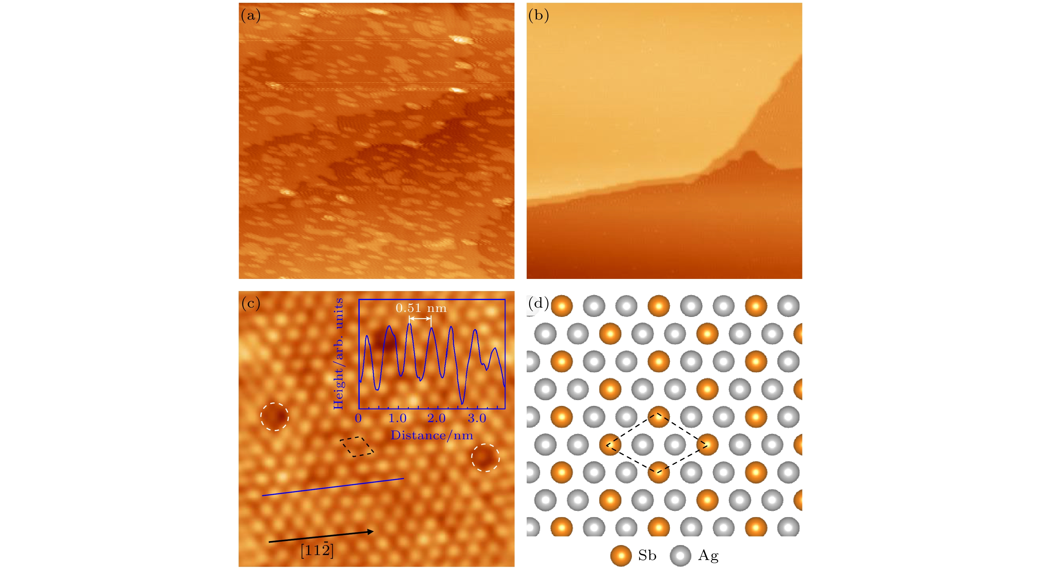
图 1 (a)室温下在Ag (111)上沉积锑原子形成纳米岛的STM形貌图(U = 1.50 V, I = 0.2 nA, 75 nm × 75 nm); (b) Ag (111)上形成Ag2Sb合金单层的大尺寸STM相貌图(U = 1.50 V, I = 0.2 nA, 65 nm × 65 nm); (c)Ag (111)上形成Ag2Sb合金单层时获得的原子分辨STM图像, 菱形表示单胞, 插图为沿着黑线测量的线轮廓 (U = 0.1 V, I = 0.1 nA, 7.4 nm × 7.4 nm); (d) Ag2Sb合金相的原子排布模型, 灰色和橙色球分别代表Ag2Sb合金相中的Ag 和Sb原子
Fig. 1. (a) STM morphology of antimony atoms deposited on Ag (111) at room temperature to form nano islands (U = 1.50 V, I = 0.2 nA, 75 nm × 75 nm); (b) large scale STM phase diagram of Ag2Sb alloy monolayer formed on Ag (111) (U = 1.50 V, I = 0.2 nA, 65 nm × 65 nm); (c) atomic resolved STM images obtained when Ag2Sb alloy monolayer is formed on Ag (111), the diamond represents a single cell, the illustration shows the contour of the line measured along the black line (U = 0.1 V, I = 0.1 nA, 7.4 nm×7.4 nm); (d) atomic arrangement model of Ag2Sb alloy phase, the gray and orange spheres represent Ag and Sb atoms in the Ag2Sb alloy phase, respectively.

图 2 (a) VOPc分子结构的侧视图和俯视图; (b)在~0.8 ML覆盖度下获得的STM形貌图 (65 nm × 65 nm, U = –1.50 V, I = –0.1 nA); (c)在~1.0 ML覆盖度下获得的STM图, 除存在少量空位外, 分子膜几乎覆盖了整个表面, 插图为相应的FFT图像 (51 nm × 51 nm, U = –0.50 V, I = –0.1 nA)
Fig. 2. (a) Side view and top view of the molecular structure of VOPc; (b) STM image obtained at the coverage of ~0.8 ML (65 nm × 65 nm, U = –1.5 V, I = –0.1 nA); (c) STM topography obtained at the coverage of ~1.0 ML, the molecular membrane covers the whole surface except the existence of small amount of vacancies, the inset shows the corresponding FFT image (51 nm × 51 nm, U = –0.50 V, I = –0.1 nA) .
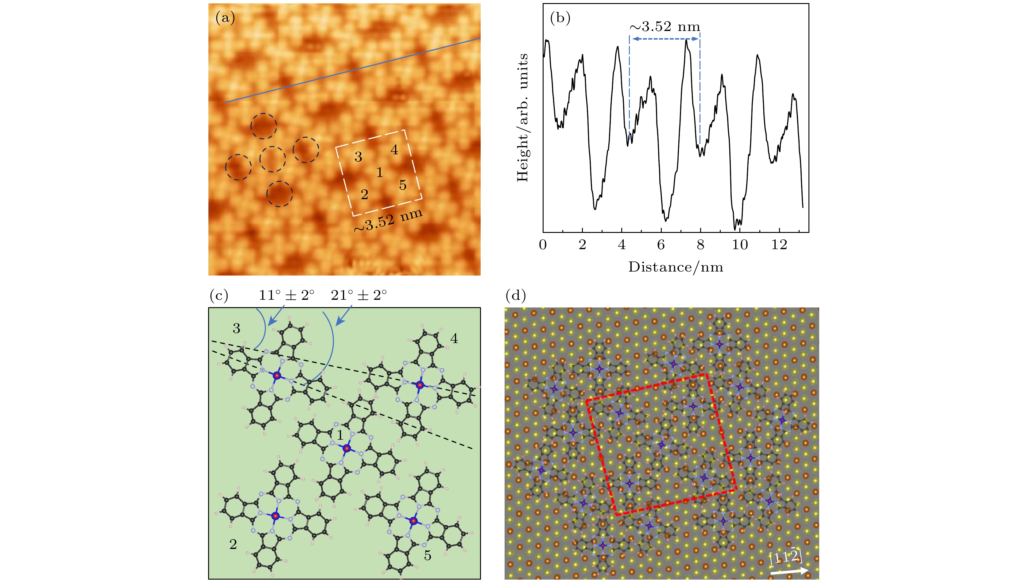
图 3 (a) VOPc分子组装结构的高分辨STM图 (14 nm×14 nm, U = –0.50 V, I = –0.1 nA); (b)沿图(a)中的蓝线测量得到的线轮廓; (c) VOPc分子膜单胞内的分子排布模型, 每个单胞由5个相互作用的分子组成, 分别用数字“1—5”表示, 分子横轴的旋转角分别为11°±2°和21°±2°; (d)在Ag2Sb/Ag(111)上, 组装VOPc分子膜的可能结构模型, 绿色和橙色球分别代表Ag2Sb合金单层中的Ag和Sb原子
Fig. 3. (a) High resolution STM image of VOPc molecular assembly structure (14 nm×14 nm, U = –0.50 V, I = –0.1 nA); (b) the line profile measured along the blue line in (a); (c) schematic molecular model of the unit cell of the assembled VOPc membrane, the unit cell consists of five molecules that are marked by the numbers “1–5”, the rotation angles of the molecular axis are about 11°±2° and 21±2°; (d) a possible structural model for assembling VOPc molecular membranes on Ag2Sb/Ag (111), the green and orange spheres represent Ag and Sb atoms in the Ag2Sb alloy monolayer, respectively.
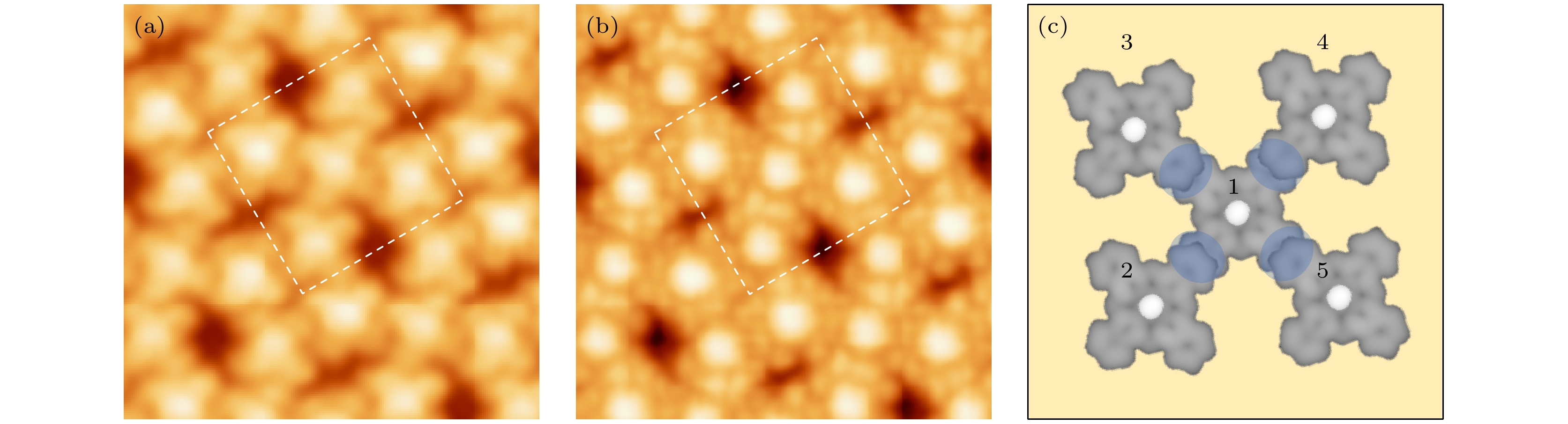
图 4 在同一区域获得的不同扫描参数VOPc分子膜的STM形貌图 (a) 8.3 nm × 8.3 nm, U = –0.50 V, I = –0.1 nA; (b) 8.3 nm × 8.3 nm, U = 0.50 V, I = 0.1 nA; (c) 分子轨道电子态分布示意图
Fig. 4. The STM morphology of VOPc molecular membranes obtained in the same region, scanning parameters: (a) 8.3 nm × 8.3 nm, U = –0.50 V, I = –0.1 nA; (b) 8.3 nm × 8.3 nm, U = 0.50 V, I = 0.1 nA; (c) schematic diagram of the electronic state distribution of molecular orbitals.
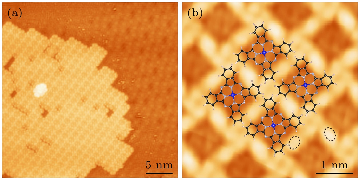
图 5 (a)在VOPc覆盖度约为1.5 ML时Ag2Sb合金单层上获得的STM形貌图(U = 1.0 V, I = 0.1 nA, 35 nm × 35 nm); (b)放大的STM图像, 虚线正方形表示单胞, 所有分子取向一致, 每个单胞只包含一个VOPc分子 (U = 1.5 V, I = 0.1 nA, 5.1 nm × 5.1 nm)
Fig. 5. (a) STM image of the VOPc molecules recorded at the coverage of about 1.5 ML on the Ag2Sb alloy (U = 1.0 V, I= 0.1 nA, 35 nm × 35 nm); (b) zoomed STM image, the dotted square denotes the unit cell (U = 1.5 V, I = 0.1 nA, 5.1 nm × 5.1 nm).
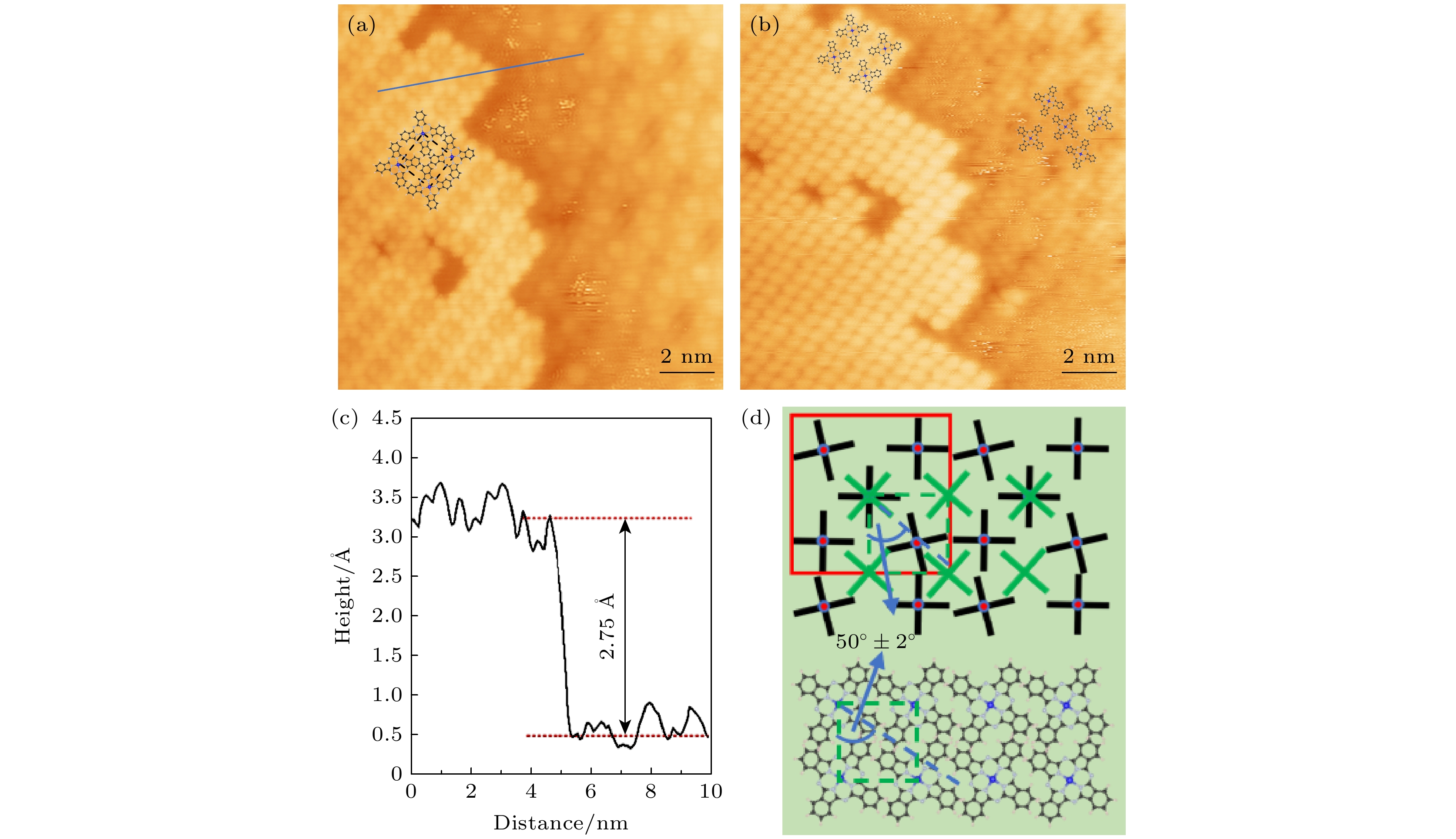
图 6 (a)同时分辨第1层分子和第2层分子的STM图像 (U = 1.0 V, I = 0.1 nA, 16.0 nm × 16.0 nm); (b)与(a)图相同区域获得的STM形貌图, 扫描偏压为负偏压 (U = –1.5 V, I = –0.1 nA, 16.0 nm × 16.0 nm); (c)沿图(a)中的蓝线测量获得的线轮廓; (d)上下两层VOPc分子排布的模型示意图, 十字叉代表VOPc分子, 第1层分子采用O-up构型(黑色十字叉), 第2层分子采用O-down构型(绿色十字叉), 两层分子的单胞分别由红色和绿色虚线正方形表示
Fig. 6. (a) STM topography obtained at a positive bias of 1.0 V, the first and second layers of VOPc molecules are simultaneously resolved (U = 1.0 V, I= 0.1 nA, 16.0 nm × 16.0 nm); (b) STM topography obtained at a negative bias of –1.5 V (U = –1.5 V, I = –0.1 nA, 16.0 nm × 16.0 nm); (c) line profile measured along the blue line in (a); (d) schematic model of the first and second layers of VOPc molecules, the forks represent the VOPc molecules, the molecules in the first layer (black forks) adopt the O-up configuration, and the molecules in the second layer (green forks) adopt the O-down configuration, the unit cells of both layers are highlighted by the red and green dotted squares, respectively.
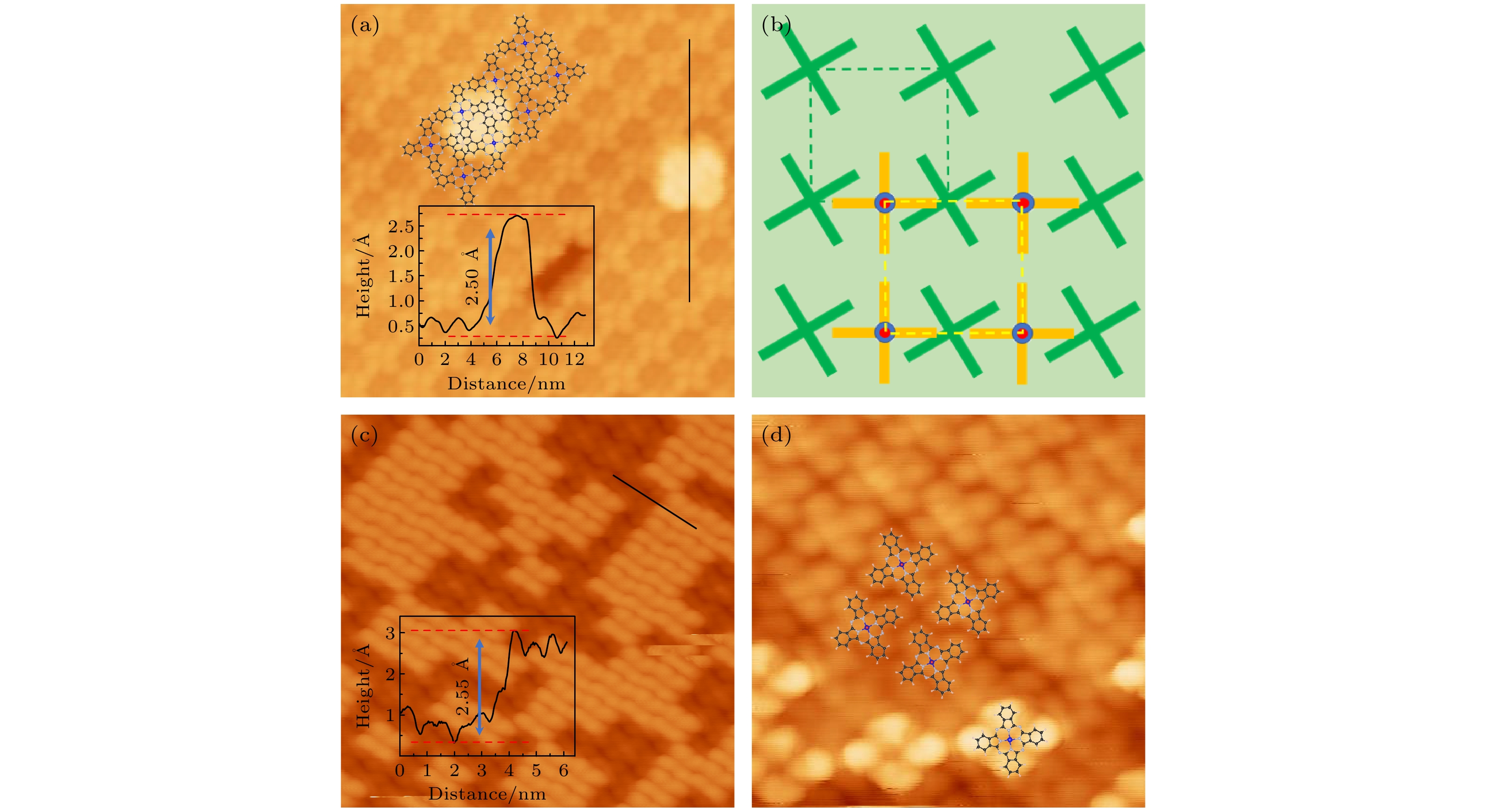
图 7 (a) 在VOPc覆盖度约为2.1 ML时获得的STM图像(U =1.0 V, I = 0.1 nA, 12.0 nm × 12.0 nm); (b)第3层分子相对第2层的结构模型, 上下两层VOPc分子用黄色和绿色十字叉表示, 虚线正方形表示相应的单胞; (c) 在VOPc覆盖度约为3.1 ML时获得的STM形貌图 (U = –1.5 V, I = –0.1 nA, 15.6 nm× 15.6 nm); (d) 在VOPc覆盖度约为3.1 ML时获得的较小尺寸的STM形貌图 (U = –1.5 V, I = –0.1 nA, 7 nm× 7 nm)
Fig. 7. (a) STM image obtained at VOPc coverage of approximately 2.1 ML (U = 1.0 V, I = 0.1 nA, 12.0 nm × 12.0 nm); (b) the structural model of the third layer molecule relative to the second layer, the upper and lower layers of VOPc molecules are represented by yellow and green crosses, the dashed square represents the corresponding unit cell; (c) STM morphology obtained at a VOPc coverage of approximately 3.1 ML (U = 1.0 V, I = 0.1 nA, 15.6 nm ×15.6 nm); (d) a smaller size STM morphology image was obtained at a VOPc coverage of approximately 3.1 ML (U = 1.0 V, I = 0.1 nA, 7 nm× 7 nm).
-
[1] Crone B, Dodabalapur A, Lin Y Y, Filas R W, Bao Z, Laduca A, Sarpeshkar R, Katz H E, Li W 2000 Nature 403 521
Google Scholar
[2] Tortech L, Fichou D, Proust A, Izzet G, Alaaeddine M 2014 Inorg. Chem. Front. 1 682
Google Scholar
[3] Blom P W M, Mihailetchi V D, Koster L J A, Markov D E 2007 Adv. Mater. 19 1551
Google Scholar
[4] Walter M G, Rudine A B, Wamser C C 2010 J. Porphyr. Phthalocya. 14 759
Google Scholar
[5] Wang H B, Song D, Yang J L, Bo Y, Geng Y H, Yan D H 2007 Appl. Phys. Lett. 90 253510
Google Scholar
[6] Ohta H, Kambayashi T, Hirano M, Hoshi H, Ishikawa K, Takezoe H, Hosono H 2003 Adv. Mater. 15 1258
Google Scholar
[7] Whitesides G M, Grzybowski B 2002 Science 295 2418
Google Scholar
[8] Xing L B, Peng Z T, Li W T, Wu K 2019 Acc. Chem. Res. 52 1048
Google Scholar
[9] Song H J, Zhu H, Huang Z C, Zhang Y J, Zhao W H, Liu J, Chen Q W, Yin C, Xing L B, Peng Z T, Liao P L, Wang Y F, Wang Y, Wu K 2019 Acs. Nano 13 7202
Google Scholar
[10] Yamaguchi S, Sasaki Y 2000 Chem. Phys. Lett. 323 35
Google Scholar
[11] Mizuguchi J, Rihs G, Karfunkel H R 1995 J. Phys. Chem. 99 16217
Google Scholar
[12] Eguchi K, Takagi Y, Nakagawa T, Yokoyama T 2013 J. Phys. Chem. C 117 22843
Google Scholar
[13] Zhu H, Song H J, Zhao W H, Peng Z T, Liu D, Xing L B, Dai J X, Huang Z C, Liao P L, Wang Y, Wu K 2019 Phys. Chem. Chem. Phys. 21 16323
Google Scholar
[14] Niu T, Zhang J, Chen W 2014 J. Phys. Chem. C 118 4151
Google Scholar
[15] Zhao W H, Zhu H, Song H J, Liu J, Chen Q, Wang Y, Wu K 2018 J. Phys. Chem. C 122 7695
Google Scholar
[16] Zhu H, Song H J, Zhao W H, Peng Z T, Liu D, Di B, Xing L B, Chen H, Huang Z C, Wang Y, Wu K 2019 J. Phys. Chem. C 123 17390
Google Scholar
[17] Blowey P, Maurer R, Rochford L, Duncan D, Kang J, Warr D, Ramadan A, Lee T, Thakur P, Costantini G 2019 J. Phys. Chem. C 123 8101
Google Scholar
[18] Lu S Z, Huang M, Qin Z H, Yu Y H, Guo Q M, Cao G Y 2018 Nanotechnology 29 315301
Google Scholar
[19] Luke A R, Alexandra J R, D Phil W, Sandrine H, Tim S J 2015 Phys. Chem. Chem. Phys. 17 29747
Google Scholar
[20] Malavolti L, Briganti M, Hänze M, Serrano G, Cimatti I, McMurtrie G, Otero E, Ohresser P, Totti F, Mannini M, Sessoli R, Loth S 2018 Nano Lett. 18 7955
Google Scholar
[21] Zhang P, Ma C, Sheng S X, Liu H R, Gao J S, Liu Z J, Cheng P, Feng B J, Chen L, Wu K H 2022 Phys. Rev. Mater. 6 074002
Google Scholar
[22] Yu Y H, Sagisaka K, Fujita D 2009 Phys. Rev. B 79 235427
Google Scholar
[23] Giordano L, Cinquini F, Pacchioni G 2006 Phys. Rev. B 73 045414
Google Scholar
[24] Shao Y, Liu Z L, Cheng C, Wu X, Liu H, Liu C, Wang J O, Zhu S Y, Wang Y Q, Shi D X, Ibrahim K, Sun J T, Wang Y L, Gao H J 2018 Nano Lett. 18 2133
Google Scholar
[25] Liu K, Bai K, Wang J, Song J, Liu Y 2022 Front. Phys. 10 856526
Google Scholar
[26] Yu Y H, Tang Z, Jiang Y, Fujita D 2008 Surf. Sci. 602 3358
Google Scholar
[27] Zhang K H L, McLeod I M, Lu Y H, Dhanak V R, Matilainen A, Lahti M, Pussi K, Egdell R G, Wang X S, Wee A T S, Chen W 2011 Phys. Rev. B 83 235418
Google Scholar
[28] Osiecki J R, Uhrberg R I G 2013 Phys. Rev. B. 87 075441
Google Scholar
[29] She L M, Yu Y H, Wu P, Zhang Y, Qin Z H, Huang M, Cao G Y 2012 J. Chem. Phys. 136 144707
Google Scholar
[30] Mattioli G, Filippone F, Amore Bonapasta A 2010 J. Phys. Chem. Lett. 1 2757
Google Scholar
[31] Fernandez L, Thussing S, Manz A, Sundermeyer J, Witte G, Jakob P 2017 Phys. Chem. Chem. Phys. 19 2495
Google Scholar
[32] Kolotovska V, Friedrich M, Zahn D R T, Salvan G 2006 J. Cryst. Growth. 291 166
Google Scholar

 下载:
下载:
计量
- 文章访问数: 4083
- PDF下载量: 79
- 被引次数: 0
