


-
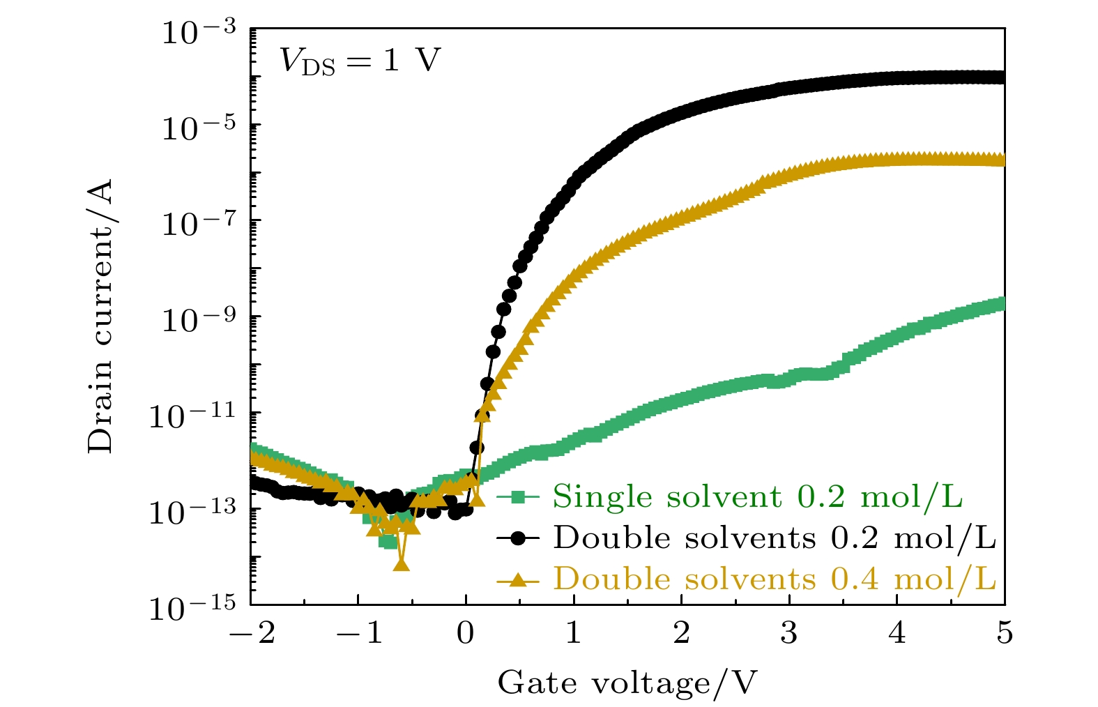
采用喷墨打印工艺制备了铟锌锡氧化物(indium-zinc-tin-oxide, IZTO)半导体薄膜, 并应用于底栅顶接触结构薄膜晶体管(thin-film transistor, TFT). 研究了墨水的溶剂成分以及溶质浓度对打印薄膜图案轮廓的影响. 结果表明二元溶剂IZTO墨水中乙二醇溶剂可有效平衡溶质向内的马兰戈尼回流与向外的毛细管流, 避免了单一溶剂墨水下溶质流动不平衡造成IZTO薄膜的咖啡环状沉积轮廓图案, 获得均匀平坦的薄膜图案轮廓和良好接触特性, 接触电阻为820 Ω, 优化后IZTO TFT器件的饱和迁移率达到16.6 cm2/(V·s), 阈值电压为0.84 V, 开关比高达3.74×10⁹, 亚阈值摆幅为0.24 V/dec. 通过打印薄膜凝胶化模型解释了IZTO墨水溶剂成分、溶质浓度与最终薄膜形貌的关系.Metal oxide thin film transistor has been widely used in flat panel display industry because of its low leakage current, high mobility and large area uniformity. Besides, with the development of printed display technology, inkjet printing process can fabricate the customizable patterns on diverse substrates with no need of vacuum or lithography to be used, thus significantly reducing cost and receiving more and more attention. In this paper, we use inkjet printing technology to prepare a bottom gate bottom contact thin film transistor (TFT) by using indium-zinc-tin-oxide (IZTO) semiconductor. The surface morphology of the printed IZTO film is modified by adjusting the solvent composition and solute concentration of the printing precursor ink. The experimental result show that the use of binary solvents can effectively overcome the coffee ring shape caused by the accumulation of solute edge in the volatilization process of a single solvent, ultimately presenting a uniform and flat contour surface. Further increase in solute concentration is in favor of formation of convex surface topology. The reason for the formation of the flat surface of the oxide film is the balance between the inward Marangoni reflux of the solute and the outward capillary flow during volatilization. In addition, IZTO thin film transistor printed with binary solvents exhibits excellent electrical properties. The ratio of width/length = 50/30 exhibits a high on-off ratio of 1.21×10⁹, a high saturation field-effect mobility is 16.6 cm2/(V·s), a low threshold voltage is 0.84 V, and subthreshold swing is 0.24 V/dec. The uniform and flat active layer thin film pattern can form good contact with the source leakage electrode, and the contact resistances of TFT devices with different width-to-length ratios are less than 1000 Ω, which can reach the basic conditions of high mobility thin film transistors prepared by inkjet printing. Therefore, using solvent mixture provides a universal and simple way to print oxide films with required surface topology, and present a visible path for inkjet printing of high-mobility thin film transistors.
[1] 荆斌, 徐萌, 彭聪, 陈龙龙, 张建华, 李喜峰 2022 物理学报 71 138502
 Google Scholar
Jing B, Xu M, Peng C, Chen L L, Zhang J H, Li X F 2022 Acta Phys. Sin. 71 138502
Google Scholar
[2] Chu S, Hollberg L, Bjorkholm J E, Bolot S, Fuchs P, Knobelspies S, Temel O, Sevilla G T, Gilshtein E, Andres C, Shorubalko I, Liu Y, Troester G, Tiwari A A N, Romanyuk Y E 2019 Adv. Electron. Mater. 5 1800843
Google Scholar
[3] Song O, Rhee D, Kim J, Jeon Y, Mazánek V, Söll A, Kwon Y A, Cho J H, Kim Y H, Kang J, Sofer Z 2022 npj 2D Mater. Appl. 6 64
Google Scholar
[4] Liang K, Li D W, Ren H H, Zhao M M, Wang H, Ding M F, Xu G W, Zhao X L, Long S B, Zhu S Y, Sheng P, Li W B, Lin X, Zhu B W 2021 Nano-Micro Lett. 13 164
Google Scholar
[5] Kwon J, Baek S, Lee Y, Tokito S, Jung S 2021 Langmuir 37 10692
Google Scholar
[6] Deegan R D, Bakajin O, Dupont T F, Huber G, Nagel S R, Witten T A 1997 Nature 389 827
Google Scholar
[7] 兰林峰, 陈宝中, 彭俊彪, 曹镛 2021 高分子材料科学与工程 37 150
Google Scholar
Lan L F, Chen B Z, Peng J B, Cao Y 2021 Polym. Mater. Sci. Eng. 37 150
Google Scholar
[8] Li Y Z, Lan L F, Gao P, He P H, Dai X, Cao H, Liang L, Peng J B 2019 IEEE Electron Device Lett. 40 228
Google Scholar
[9] Ryu S O, Ha C H, Jun H Y, Ryu S O 2020 J. Electron. Mater. 49 2003
Google Scholar
[10] Gillan L, Li S, Lahtinen J, Chang C H, Alastalo A, Leppäniemi J 2021 Adv. Mater. Interfaces 8 2100728
Google Scholar
[11] Matavz A, Ursic U, Mocivnik J, Richter D, Humar M, Copar S, Malic B, Bobnar V 2022 J. Colloid Interface Sci. 608 1718
Google Scholar
[12] Sun D W, Chen C H, Zhang J, Wu X M, Chen H P, Guo T L 2018 Appl. Phys. Lett. 112 012102
Google Scholar
[13] Zhu Z N, Zhang J H, Zhou Z W, Ning H L, Cai W, Wei J L, Zhou S X, Yao R H, Lu X B, Peng J B A 2019 ACS Appl. Mater. Interfaces 11 5193
Google Scholar
[14] Zhu Z N, Ning H L, Cai W, Wei J L, Zhou S X, Yao R H, Lu X B, Zhang J H, Zhou Z W, Peng J B A 2018 Langmuir 34 6413
Google Scholar
[15] Still T, Yunker P J, Yodh A G 2012 Langmuir 28 4984
Google Scholar
[16] Hu H L, Zhu J G, Chen M S, Guo T L, Li F S 2018 Appl. Surf. Sci. 441 295
Google Scholar
[17] Zhong X, Duan F 2016 Eur. Phys. J. B 39 18
Google Scholar
[18] Oh G, Jeong W, Jung N, Kang S H, Weon B M 2022 Phys. Rev. Appl. 17 024010
Google Scholar
[19] Kim D, Jeong S, Park B K, Moon J 2006 Appl. Phys. Lett. 89 264101
Google Scholar
[20] Kim M G, Kim H S, Ha Y G, He J Q, Kanatzidis M G, Facchetti A, Marks T J 2010 J. Am. Chem. Soc. 132 10352
Google Scholar
[21] 朱乐永, 高娅娜, 李喜峰, 张建华 2015 物理学报 64 168501
Google Scholar
Zhu L Y, Gao Y N, Zhang J H, Li X F 2015 Acta Phys. Sin. 64 168501
Google Scholar
[22] Choi S, Kim K T, Park S K, Kim Y H 2019 Materials 12 852
Google Scholar
[23] Friederich A, Binder J R, Bauer W 2013 J. Am. Ceram. Soc. 96 2093
Google Scholar
[24] Ishizuka H, Fukai J 2018 Exp. Fluids 59 4
Google Scholar
[25] Li Y Z, He P H, Chen S T, Lan L F, Dai X Q, Peng J B 2019 ACS Appl. Mater. Interfaces 11 28052
Google Scholar
[26] Park J, Moon J 2006 Langmuir 22 3506
Google Scholar
[27] Huang H, Hu H L, Zhu J G, Guo T L 2017 J. Electron. Mater. 46 4497
Google Scholar
[28] 陶洪, 罗浩德, 宁洪龙, 姚日晖, 蔡炜, 郑喜凤, 汪洋, 王铂, 曹慧, 彭俊彪 2021 液晶与显示 36 663
Google Scholar
Tao H, Luo H D, Ning H L, Yao R H, Cai W, Zheng X F, Wang Y, Wang B, Cao H, Peng, J B 2021 Chin. J. Liq. Cryst. Disp. 36 663
Google Scholar
[29] Chen S T, Li Y Z, Lin Y L, He P H, Long T, Deng C H, Chen Z, Chen G S, Tao H, Lan L F, Peng J B 2020 Coatings 10 425
Google Scholar
[30] Fan C L, Hsin T C, Yu X W, Lin Z C 2024 Mater. Sci. Semicond. Process. 172 1396
Google Scholar
[31] Weber C, Oberberg M, Weber D, Bock C, Pham D V, Kunze U 2014 Adv. Mater. Interfaces 1 1400137
Google Scholar
[32] 林奕龙, 陈思婷, 吴永波, 兰林锋, 彭俊彪 2021 液晶与显示 36 1239
Google Scholar
Lin Y L, Chen S T, Wu Y B, Lan L F, Peng J B A 2021 Chin. J. Liq. Cryst. Disp. 36 1239
Google Scholar
-

图 1 IZTO TFT器件的光学显微镜图像, 插图显示截面示意图
Fig. 1. Microscope images of the IZTO TFT device, where the inset shows the schematic cross section.
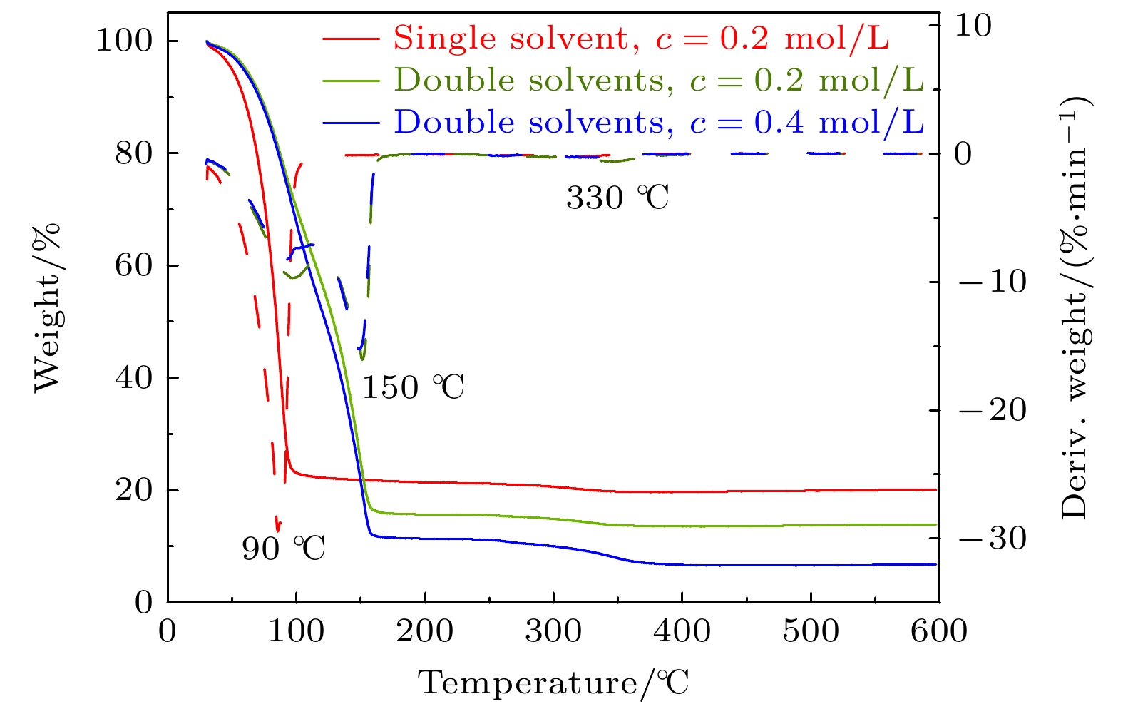
图 2 IZTO前驱体墨水的热重曲线(实线)和热重微分曲线(虚线)
Fig. 2. The TGA curve (solid lines) and DTG curve (dotted lines) of IZTO precursor ink.
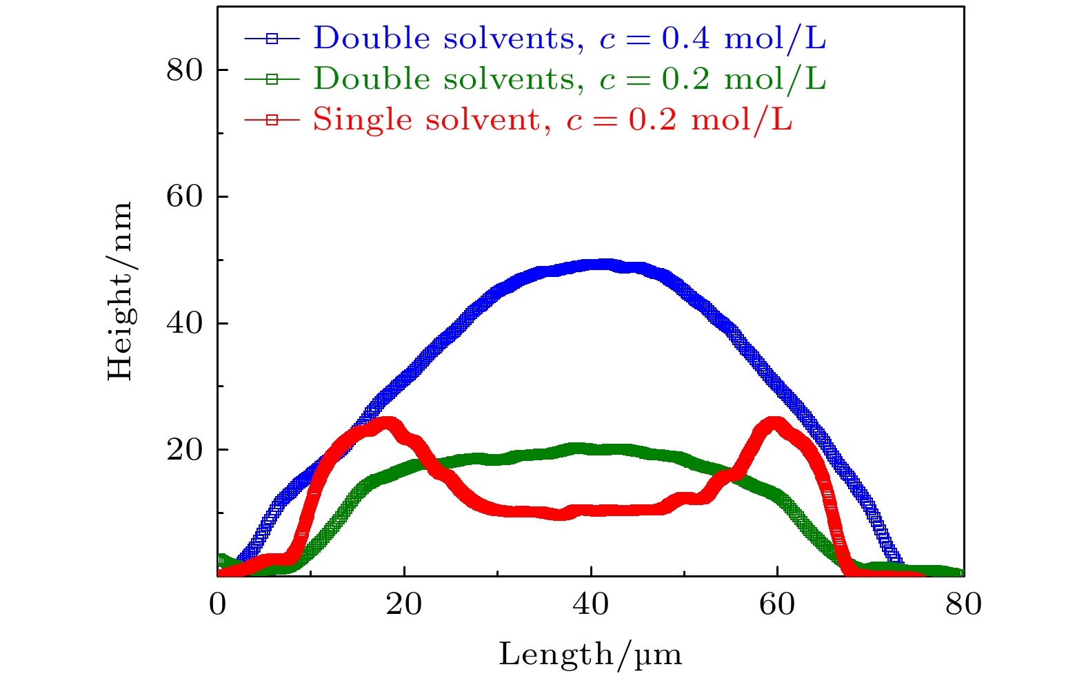
图 3 不同溶剂、不同浓度下的IZTO薄膜的表面轮廓图
Fig. 3. Surface profiles of IZTO films with different solvents and concentrations.

图 5 (a) 单溶剂和(b)二元溶剂制备IZTO薄膜的O 1s峰的XPS光谱
Fig. 5. XPS spectra of O 1s peaks of IZTO films prepared with (a) single solvent and (b) binary solvents.
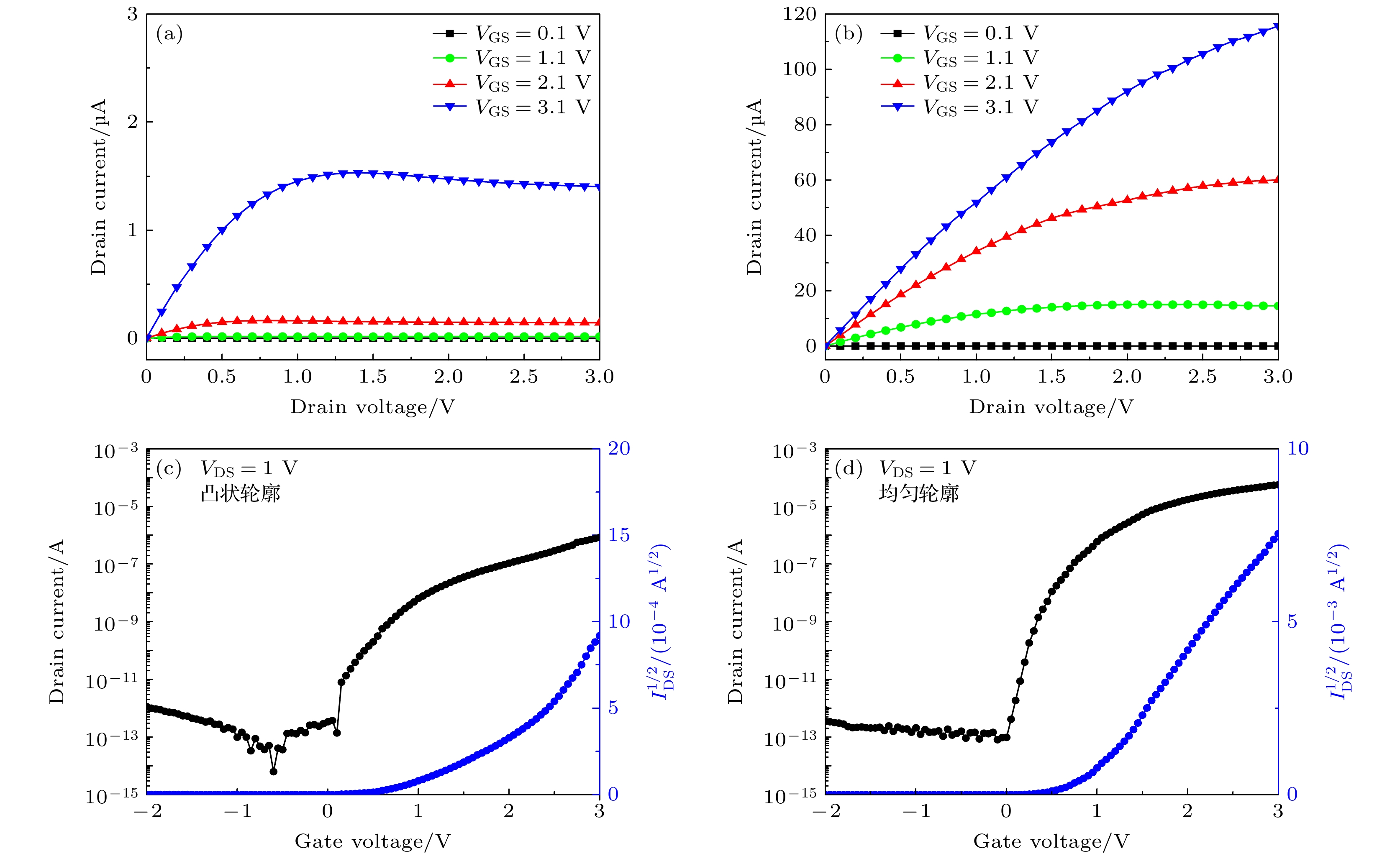
图 7 IZTO TFT器件的(a), (b)输出与(c), (d)转移曲线 (a), (c)凸状轮廓; (b), (d)平坦轮廓
Fig. 7. (a), (b) Output and (c), (d) transfer curves of IZTO TFT device: (a), (c) Convex profile and (b), (d) uniform flat profile.
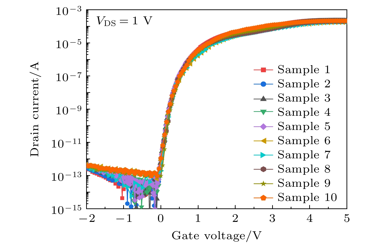
图 8 喷墨打印10个IZTO TFT器件的转移特性曲线汇总图
Fig. 8. Summary of transfer characteristic curves of 10 IZTO TFT devices fabricated by inkjet printing.
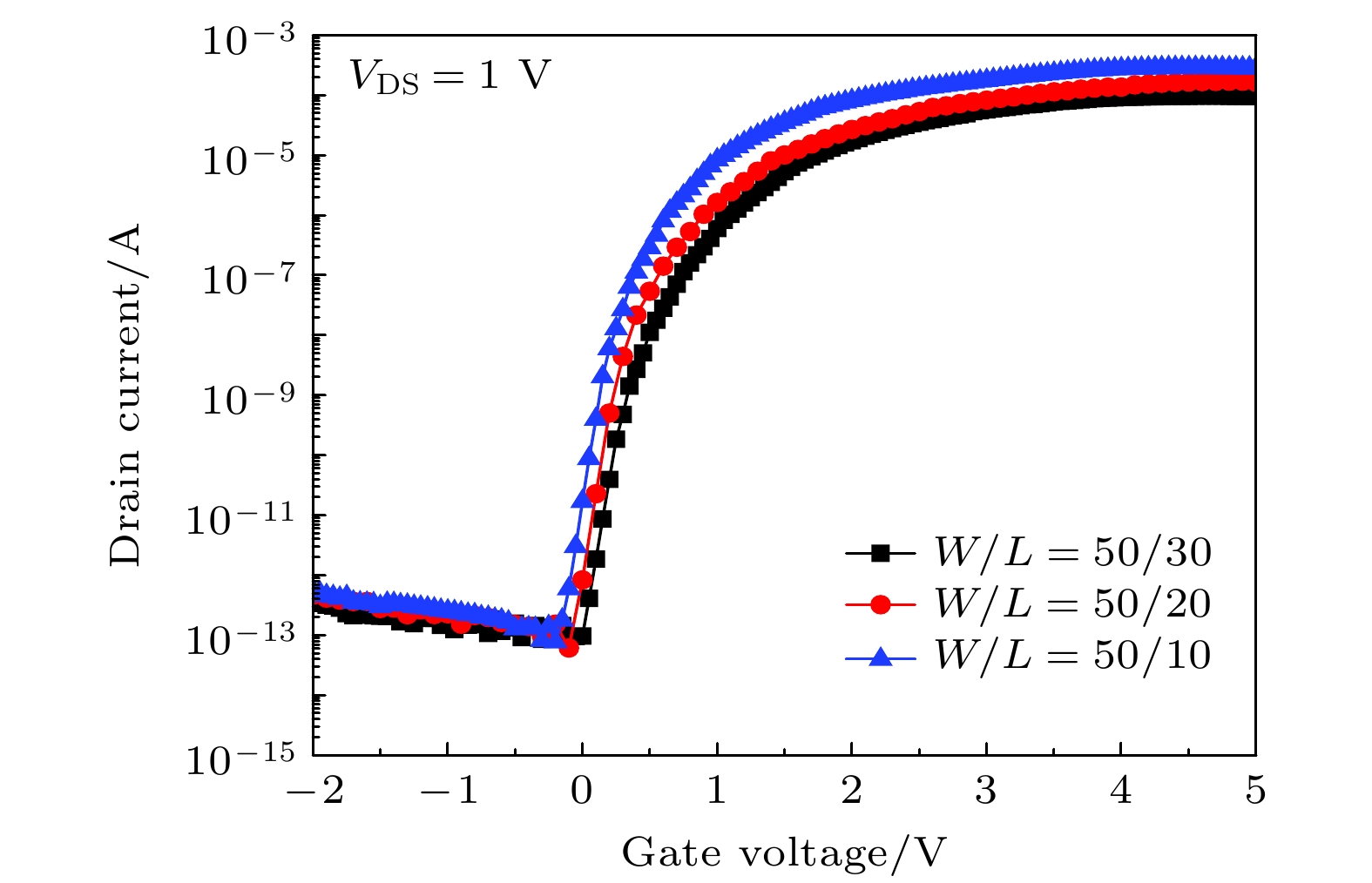
图 9 不同沟道宽长比的IZTO TFT器件的转移特性曲线
Fig. 9. Transfer characteristic curves of IZTO TFT devices with different aspect ratios.
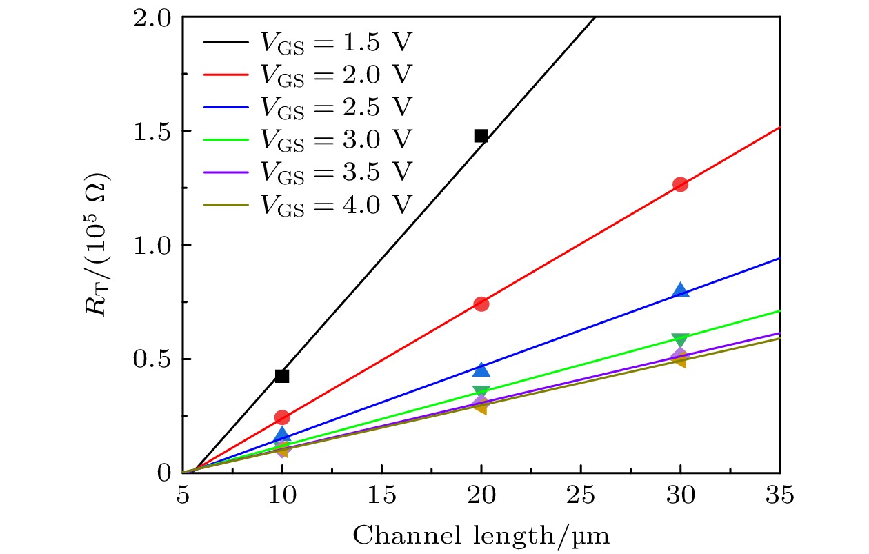
图 10 沟道长度为10—30 μm时IZTO TFT 获得的总电阻与沟道长度(RT-L)图
Fig. 10. Total resistance vs. channel length (RT-L) plots obtained from IZTO TFTs with a channel length of 10–30 μm.
表 1 不同浓度、溶剂下对应的IZTO墨水的物理参数
Table 1. Structural parameters of IZTO ink of different concentration and solvents.
IZTO墨水样品 ρ/(g·cm–3) η/cP γ/(mN·m–1) Z c = 0.2 mol/L,
2-MOE1.04 4.05 34.4 6.59 c = 0.2 mol/L,
2-MOE+EG1.07 6.90 38.1 4.14 c = 0.4 mol/L,
2-MOE+EG1.10 8.44 39.1 3.48  下载: 导出CSV
表 2 喷墨打印法制备TFT器件的性能对比
Table 2. Performance comparison of TFT devices prepared by inkjet printing method.
下载: 导出CSV
表 3 喷墨打印IZTO TFT的电性能参数平均值
Table 3. Average electrical performance parameters of inkjet printed IZTO TFT.
μ/(cm2·V–1·s–1) VTH/V S.S/(mV·dec–1) Average value 11 ± 2 0.6 ± 0.15 90 ± 15
下载: 导出CSV
表 4 不同沟道宽长比的IZTO为有源层TFT器件性能对比
Table 4. Structural parameters of IZTO TFT devices with different aspect ratios.
W/L μsat/
(cm2·V–1·s–1)VTH/
VS.S/(V·dec–1) Ion/Ioff 50/30 16.6 0.84 0.24 1.21×10⁹ 50/20 14.9 0.73 0.15 2.79×10⁹ 50/10 11.5 0.57 0.10 3.74×10⁹
下载: 导出CSV
-
[1] 荆斌, 徐萌, 彭聪, 陈龙龙, 张建华, 李喜峰 2022 物理学报 71 138502
Google Scholar
Jing B, Xu M, Peng C, Chen L L, Zhang J H, Li X F 2022 Acta Phys. Sin. 71 138502
Google Scholar
[2] Chu S, Hollberg L, Bjorkholm J E, Bolot S, Fuchs P, Knobelspies S, Temel O, Sevilla G T, Gilshtein E, Andres C, Shorubalko I, Liu Y, Troester G, Tiwari A A N, Romanyuk Y E 2019 Adv. Electron. Mater. 5 1800843
Google Scholar
[3] Song O, Rhee D, Kim J, Jeon Y, Mazánek V, Söll A, Kwon Y A, Cho J H, Kim Y H, Kang J, Sofer Z 2022 npj 2D Mater. Appl. 6 64
Google Scholar
[4] Liang K, Li D W, Ren H H, Zhao M M, Wang H, Ding M F, Xu G W, Zhao X L, Long S B, Zhu S Y, Sheng P, Li W B, Lin X, Zhu B W 2021 Nano-Micro Lett. 13 164
Google Scholar
[5] Kwon J, Baek S, Lee Y, Tokito S, Jung S 2021 Langmuir 37 10692
Google Scholar
[6] Deegan R D, Bakajin O, Dupont T F, Huber G, Nagel S R, Witten T A 1997 Nature 389 827
Google Scholar
[7] 兰林峰, 陈宝中, 彭俊彪, 曹镛 2021 高分子材料科学与工程 37 150
Google Scholar
Lan L F, Chen B Z, Peng J B, Cao Y 2021 Polym. Mater. Sci. Eng. 37 150
Google Scholar
[8] Li Y Z, Lan L F, Gao P, He P H, Dai X, Cao H, Liang L, Peng J B 2019 IEEE Electron Device Lett. 40 228
Google Scholar
[9] Ryu S O, Ha C H, Jun H Y, Ryu S O 2020 J. Electron. Mater. 49 2003
Google Scholar
[10] Gillan L, Li S, Lahtinen J, Chang C H, Alastalo A, Leppäniemi J 2021 Adv. Mater. Interfaces 8 2100728
Google Scholar
[11] Matavz A, Ursic U, Mocivnik J, Richter D, Humar M, Copar S, Malic B, Bobnar V 2022 J. Colloid Interface Sci. 608 1718
Google Scholar
[12] Sun D W, Chen C H, Zhang J, Wu X M, Chen H P, Guo T L 2018 Appl. Phys. Lett. 112 012102
Google Scholar
[13] Zhu Z N, Zhang J H, Zhou Z W, Ning H L, Cai W, Wei J L, Zhou S X, Yao R H, Lu X B, Peng J B A 2019 ACS Appl. Mater. Interfaces 11 5193
Google Scholar
[14] Zhu Z N, Ning H L, Cai W, Wei J L, Zhou S X, Yao R H, Lu X B, Zhang J H, Zhou Z W, Peng J B A 2018 Langmuir 34 6413
Google Scholar
[15] Still T, Yunker P J, Yodh A G 2012 Langmuir 28 4984
Google Scholar
[16] Hu H L, Zhu J G, Chen M S, Guo T L, Li F S 2018 Appl. Surf. Sci. 441 295
Google Scholar
[17] Zhong X, Duan F 2016 Eur. Phys. J. B 39 18
Google Scholar
[18] Oh G, Jeong W, Jung N, Kang S H, Weon B M 2022 Phys. Rev. Appl. 17 024010
Google Scholar
[19] Kim D, Jeong S, Park B K, Moon J 2006 Appl. Phys. Lett. 89 264101
Google Scholar
[20] Kim M G, Kim H S, Ha Y G, He J Q, Kanatzidis M G, Facchetti A, Marks T J 2010 J. Am. Chem. Soc. 132 10352
Google Scholar
[21] 朱乐永, 高娅娜, 李喜峰, 张建华 2015 物理学报 64 168501
Google Scholar
Zhu L Y, Gao Y N, Zhang J H, Li X F 2015 Acta Phys. Sin. 64 168501
Google Scholar
[22] Choi S, Kim K T, Park S K, Kim Y H 2019 Materials 12 852
Google Scholar
[23] Friederich A, Binder J R, Bauer W 2013 J. Am. Ceram. Soc. 96 2093
Google Scholar
[24] Ishizuka H, Fukai J 2018 Exp. Fluids 59 4
Google Scholar
[25] Li Y Z, He P H, Chen S T, Lan L F, Dai X Q, Peng J B 2019 ACS Appl. Mater. Interfaces 11 28052
Google Scholar
[26] Park J, Moon J 2006 Langmuir 22 3506
Google Scholar
[27] Huang H, Hu H L, Zhu J G, Guo T L 2017 J. Electron. Mater. 46 4497
Google Scholar
[28] 陶洪, 罗浩德, 宁洪龙, 姚日晖, 蔡炜, 郑喜凤, 汪洋, 王铂, 曹慧, 彭俊彪 2021 液晶与显示 36 663
Google Scholar
Tao H, Luo H D, Ning H L, Yao R H, Cai W, Zheng X F, Wang Y, Wang B, Cao H, Peng, J B 2021 Chin. J. Liq. Cryst. Disp. 36 663
Google Scholar
[29] Chen S T, Li Y Z, Lin Y L, He P H, Long T, Deng C H, Chen Z, Chen G S, Tao H, Lan L F, Peng J B 2020 Coatings 10 425
Google Scholar
[30] Fan C L, Hsin T C, Yu X W, Lin Z C 2024 Mater. Sci. Semicond. Process. 172 1396
Google Scholar
[31] Weber C, Oberberg M, Weber D, Bock C, Pham D V, Kunze U 2014 Adv. Mater. Interfaces 1 1400137
Google Scholar
[32] 林奕龙, 陈思婷, 吴永波, 兰林锋, 彭俊彪 2021 液晶与显示 36 1239
Google Scholar
Lin Y L, Chen S T, Wu Y B, Lan L F, Peng J B A 2021 Chin. J. Liq. Cryst. Disp. 36 1239
Google Scholar

 下载:
下载:
计量
- 文章访问数: 5352
- PDF下载量: 144
- 被引次数: 0
