-
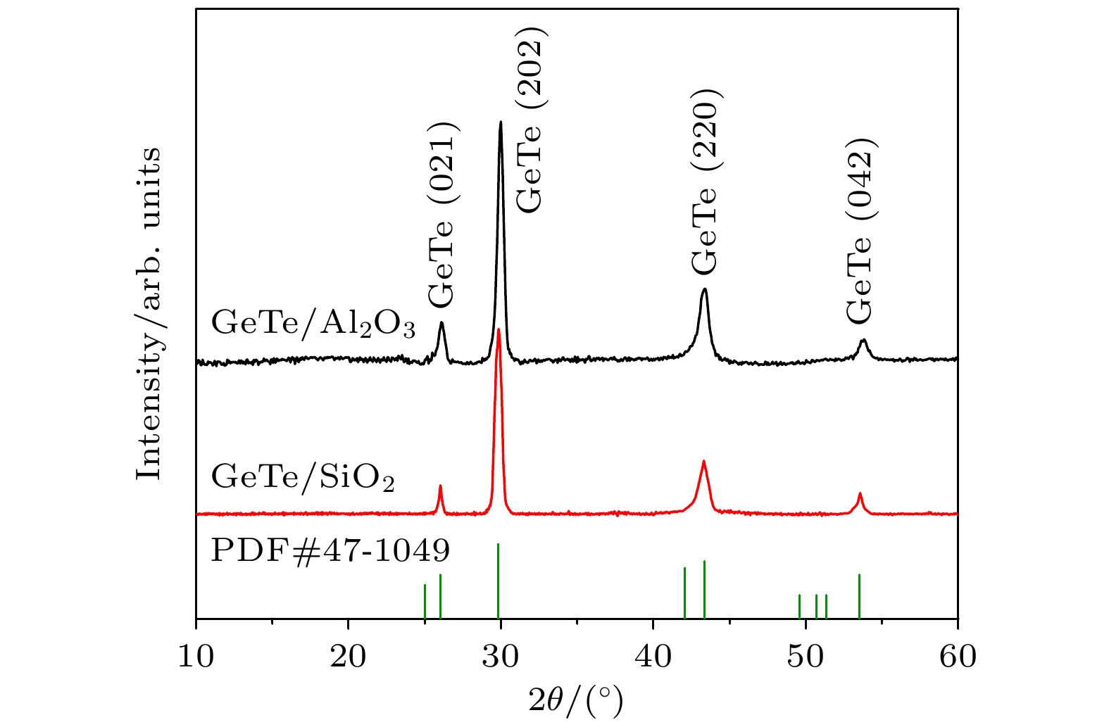
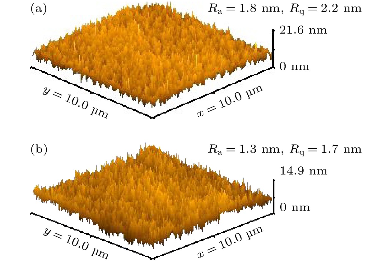
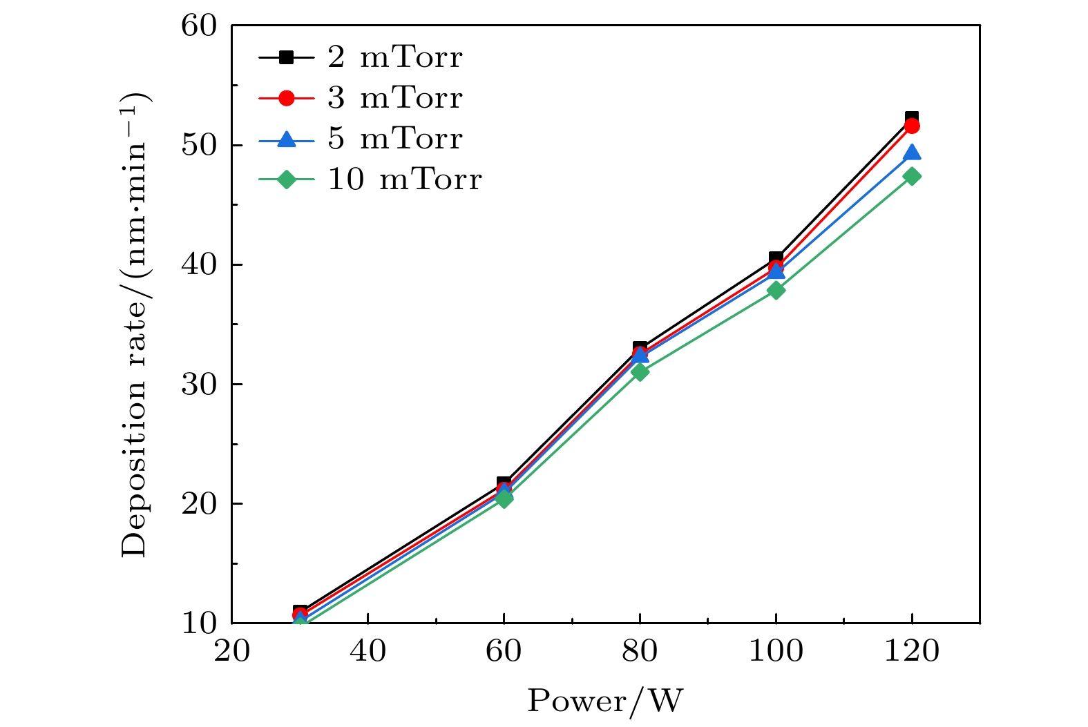
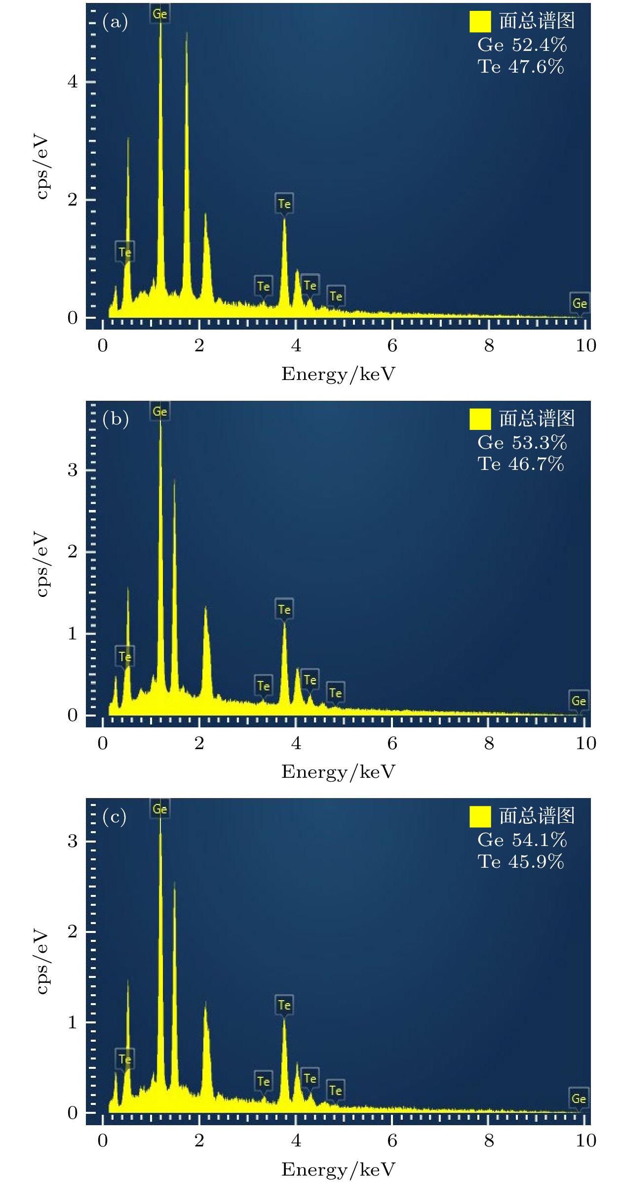
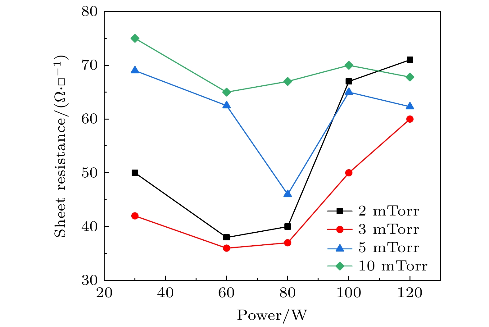
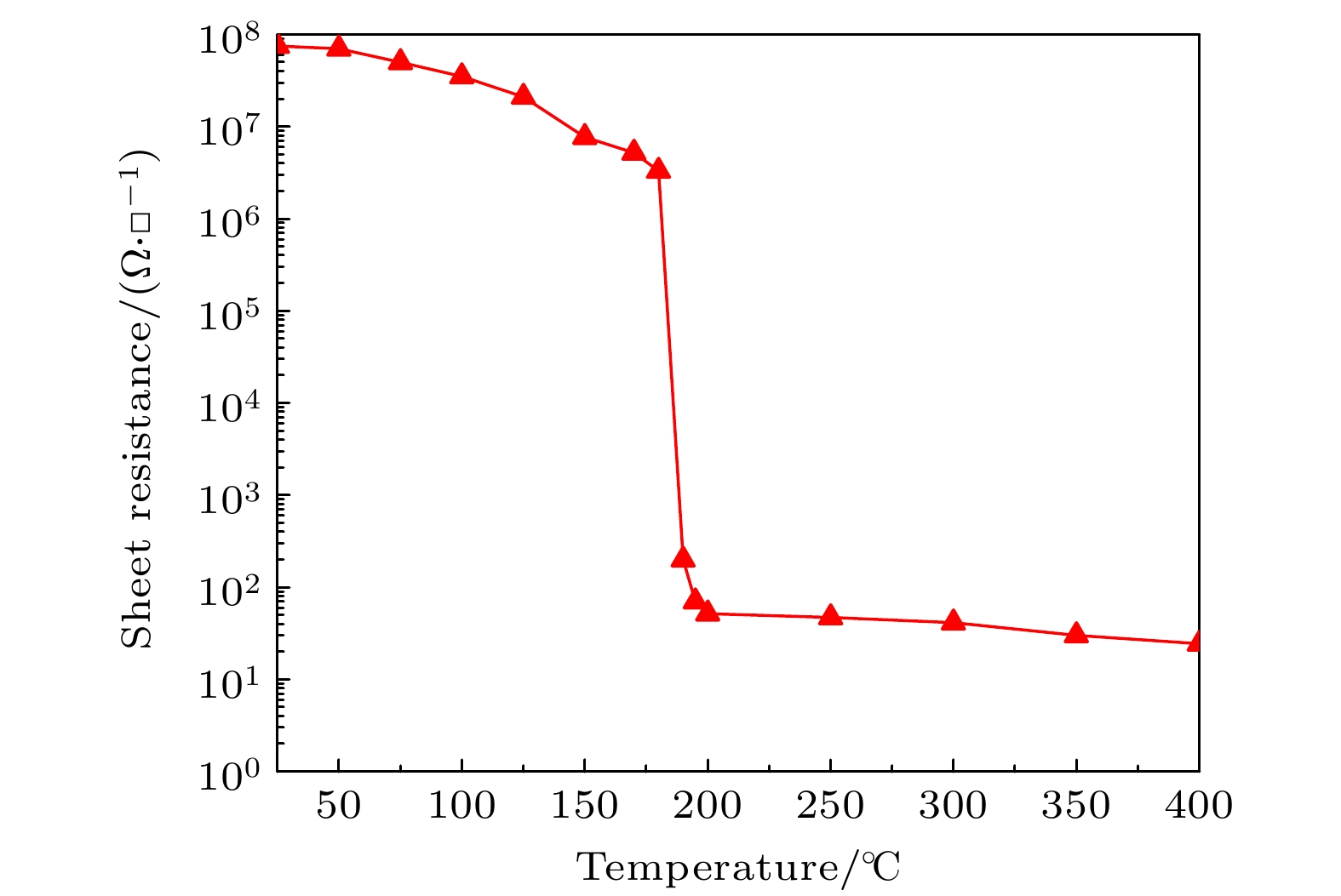
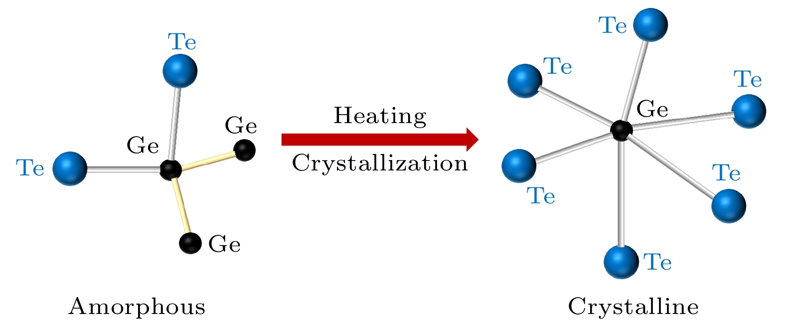
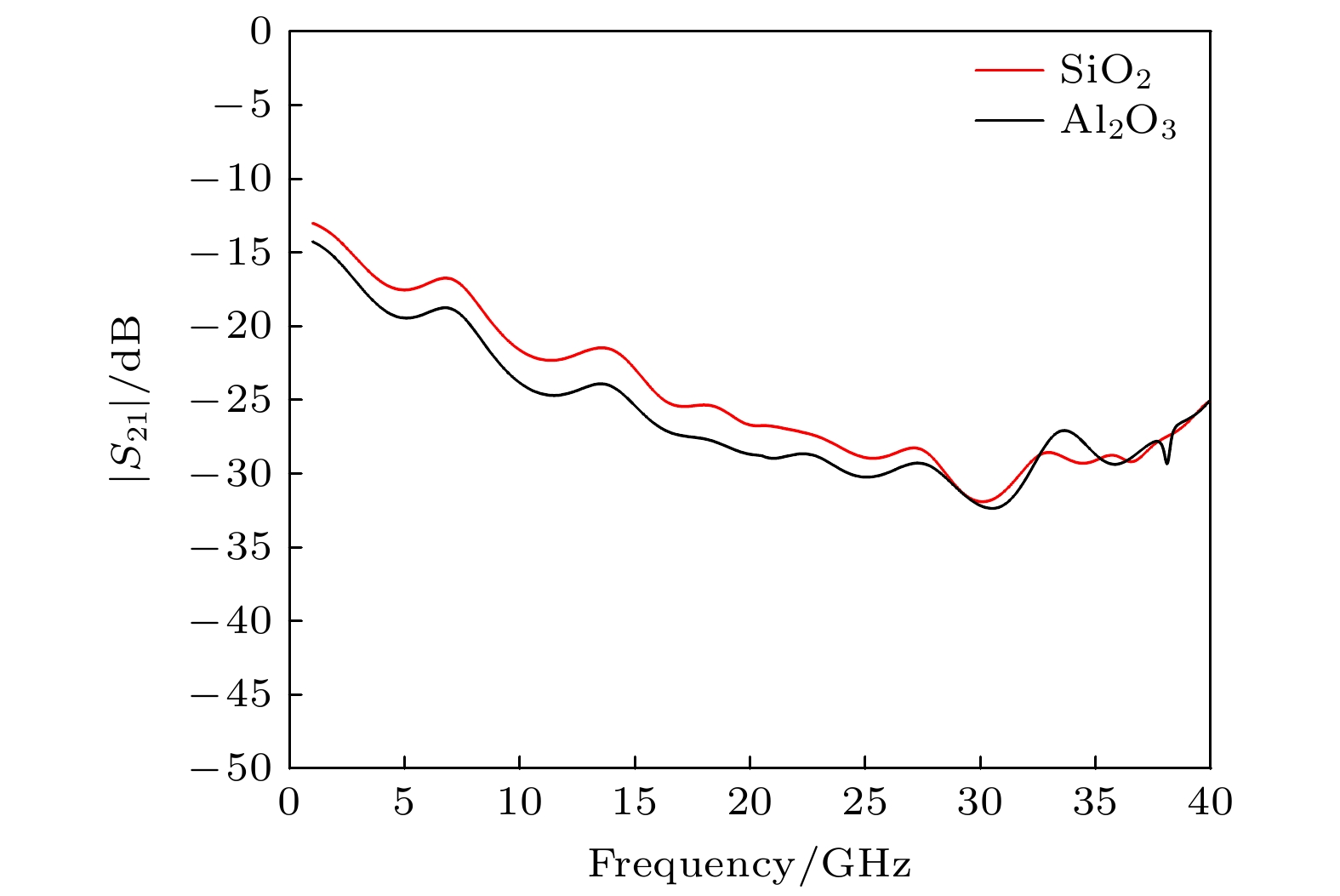
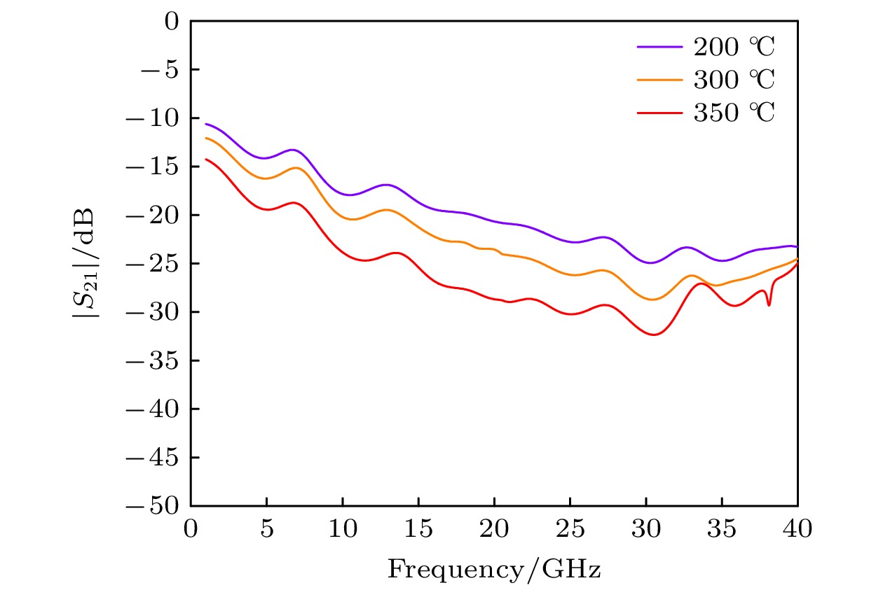
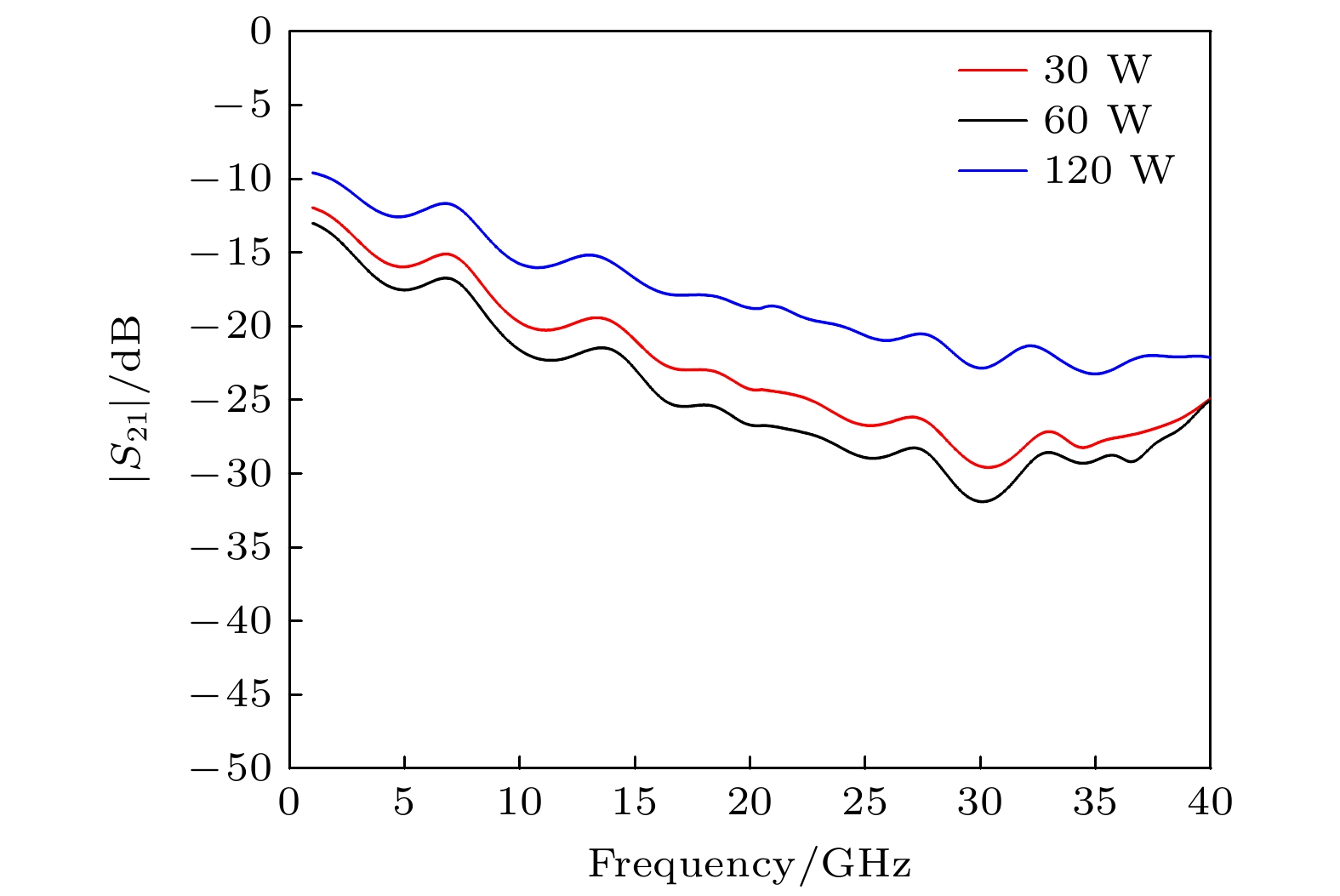
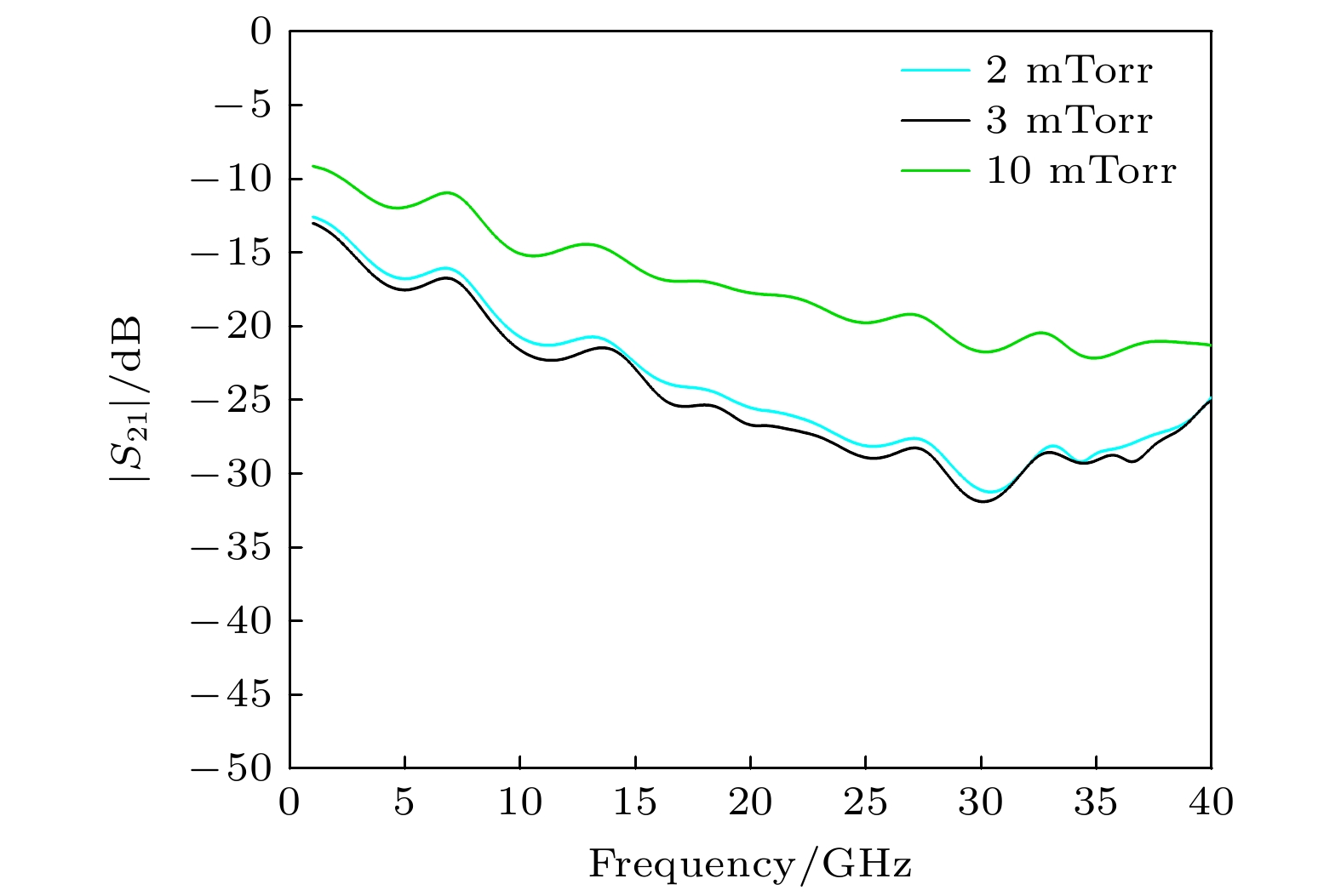
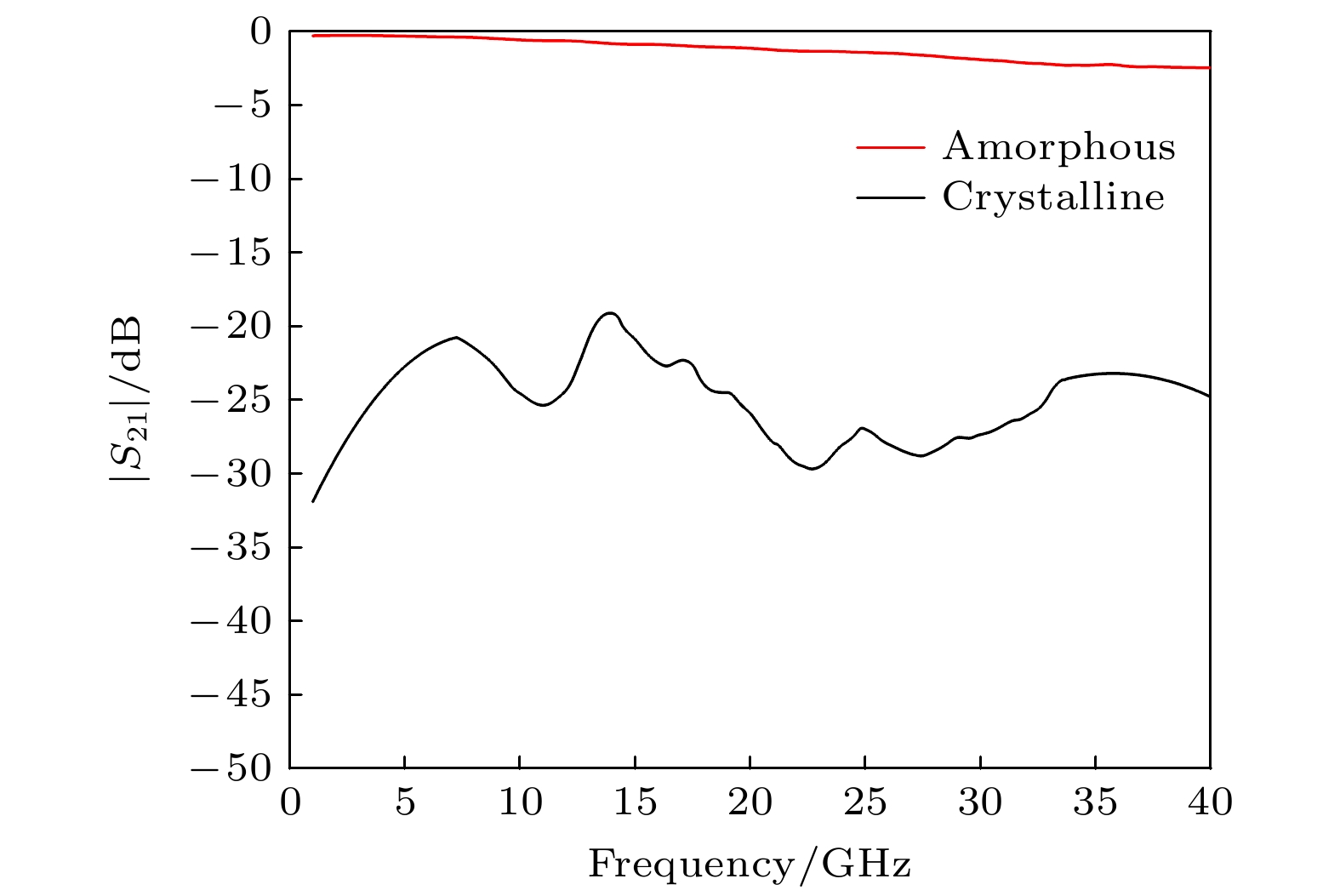
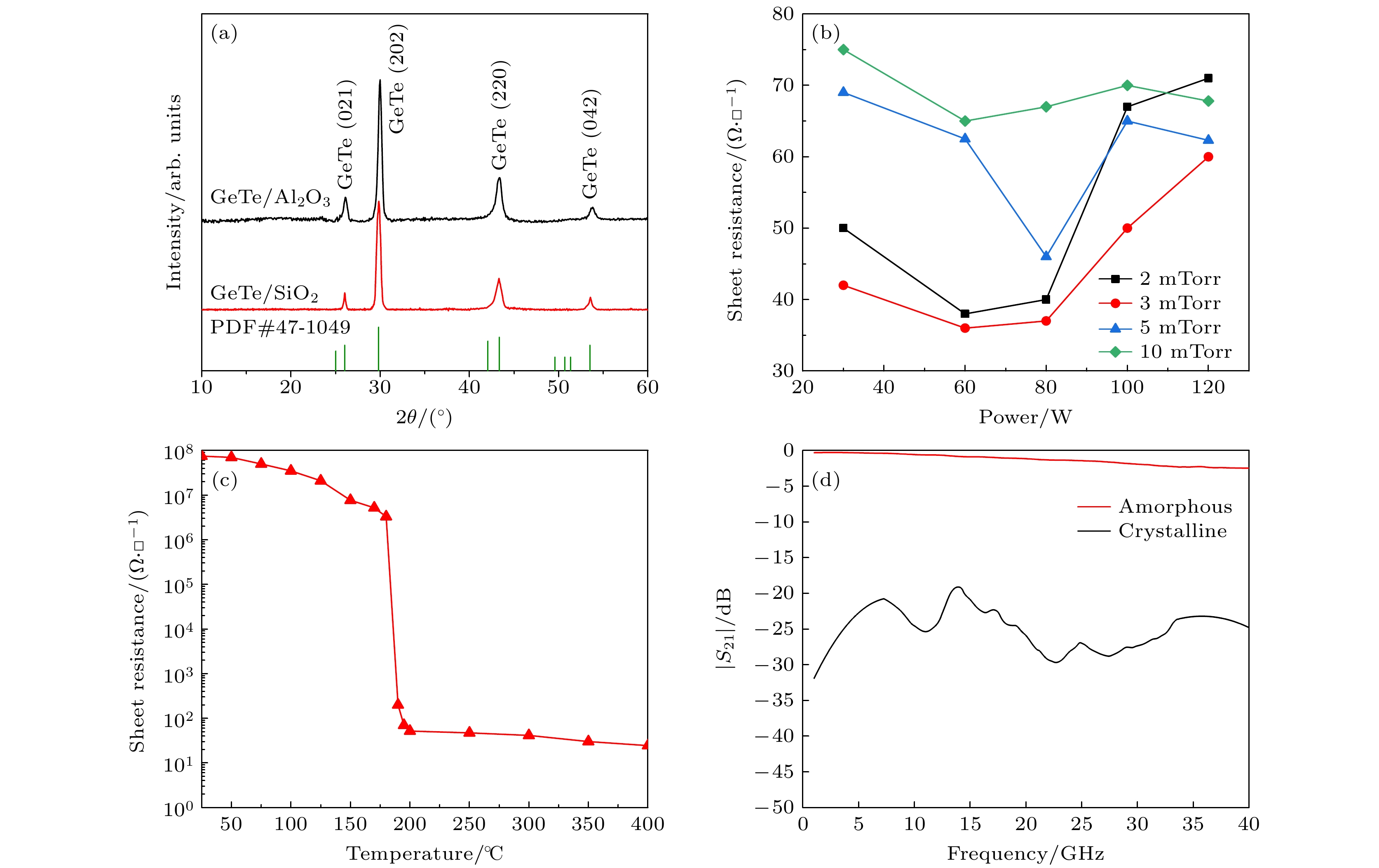
GeTe属于硫系相变材料中的一种, 利用热致相变特性可以动态实现低电阻率的晶态与高电阻率的非晶态之间可逆切换, 是忆阻器和非易失射频开关领域的重要功能材料. 本文以面向射频开关应用为出发点, 重点对磁控溅射制备的GeTe薄膜进行电性能优化研究. 通过综合分析衬底材料、溅射条件以及退火条件等因素对晶态GeTe薄膜电阻率的影响, 探索出低电阻率GeTe薄膜的有效制备条件. 结果表明, 制备的GeTe薄膜最低晶态电阻率达到3.6×10⁻⁶ Ω·m, 电阻比大于106. 此外, 基于规则的方形薄膜切片, 构建了一款零静态功耗并联型毫米波开关, 在1—40 GHz频带内, 插损小于2.4 dB, 隔离度大于19 dB, 展示了GeTe薄膜在宽带高性能分立式非易失射频开关领域的应用潜力.GeTe belongs to a chalcogenide phase change material, which can dynamically achieve reversible switching between the crystalline state of low resistivity and the amorphous state of high resistivity by utilizing the thermally induced phase change characteristics. The GeTe is an important functional material in the fields of memristors and nonvolatile radio frequency (RF) switches. For RF switch applications, this paper focuses on optimizing the electrical performance of GeTe thin films prepared by magnetron sputtering. By comprehensively analyzing the effects of substrate materials, sputtering conditions, and annealing conditions on the resistivity of crystalline GeTe films, effective conditions for preparing low resistivity GeTe films are explored. Fig. (a) shows that compared with the GeTe film on a SiO2 substrate, the film on an Al2O3 substrate can obtain higher crystallinity and lower resistivity. For the deposition power and pressure shown in Fig. (b), the combination of medium power (50–80 W) and low pressure (2–3 mTorr) is beneficial for low crystalline resistivity of GeTe film. Additionally, Fig. (c) shows that higher annealing temperature (350–400 ℃) can realize lower film resistivity. Finally, the experimental results show that the lowest crystalline resistivity of the prepared GeTe thin film reaches 3.6×10⁻⁶ Ω·m, and the resistance ratio is more than 106. Based on rectangular chips of GeTe film, a parallel millimeter-wave switch with zero static power is also constructed. As shown in Fig. (d), the insertion loss is less than 2.4 dB, and the isolation is greater than 19 dB in a 1–40 GHz frequency band, demonstrating the potential application of GeTe thin films in the field of broadband high-performance discrete nonvolatile RF switches.
-
Keywords:
- GeTe film /
- thermally induced phase change /
- radio frequency switch /
- discrete
[1] Rangan S, Rappaport T S, Erkip E 2014 Proc. IEEE 102 366
 Google Scholar
[2] Wu Z Y, Lu W, Bao X Y, Meng F B, Yang Z B, Sun Q, Zhao F Z, Wang Y T 2021 Int. J. Mod. Phys. B 35 15017
 Google Scholar
[3] Sun P, Upadhyaya P, Jeong D, Jeong D H, Heo D, La Rue G S 2007 IEEE Microw. Wirel. Co. 17 352
 Google Scholar
[4] Doan C H, Emami S, Niknejad A M, Brodersen R W 2005 IEEE J. Solid-State Circuits 40 144
 Google Scholar
[5] Wolf R, Joseph A, Botula A, Slinkman J 2009 IEEE Topical Meeting on Silicon Monolithic Integrated Circuits in RF Systems San Diego, USA, January 19–21, 2009 p1
[6] Campbell C F, Dumka D C 2010 IEEE MTT-S International Microwave Symposium Anaheim, USA, May 23–28, 2010 p145
[7] Daneshmand M, Mansour R R 2011 IEEE Microw. Mag. 12 92
 Google Scholar
[8] Boles T, Brogle J, Hoag D, Curcio D 2011 IEEE International Conference on Microwaves, Communications, Antennas and Electronic Systems (COMCAS 2011) Tel Aviv, Israel, November 7–9, 2011 p1
[9] Jaffe M, Abou-Khalil M, Botula A, Ellis-Monaghan J, Gambino J, Gross J, He Z X, Joseph A, Phelps R, Shank S, Slinkman J, Wolf R 2015 IEEE 15th Topical Meeting on Silicon Monolithic Integrated Circuits in RF Systems San Diego, USA, January 26–28, 2015 p30
[10] Stefanini R, Chatras M, Blondy P, Rebeiz G M 2011 IEEE MTT-S International Microwave Symposium Digest, Baltimore MD, USA, June 5–10, 2011 p1
[11] Grant P, Denhoff M, Mansour R R 2004 Proceedings of the IEEE International Conference on MEMS, NANO and Smart Systems (ICMENS) Banff, Canada, August 25–27, 2004 p515
[12] Tabata O, Tsuchiya T 2014 Reliability of MEMS: Testing of Materials and Devices (Hoboken: John Wiley & Sons) pp124–130
[13] Pan K, Wang W, Shin E, Freeman K, Subramanyam G 2015 IEEE T. Electron Dev. 62 2959
 Google Scholar
[14] Morin F J 1959 Phys. Rev. Lett. 3 34
 Google Scholar
[15] Bahl S K, Chopra K L 1970 J. Appl. Phys. 41 2196
 Google Scholar
[16] Raoux S, Cheng H Y, Munoz B, Jordan-Sweet J 2009 European Phase Change and Ovonic Science Symposium, 2009 p91
[17] Raoux S, Ielmini D, Wuttig M, Karpov I 2012 MRS Bull. 37 118
 Google Scholar
[18] Raoux S, Cheng H Y, Caldwell M A, Wong H S P 2009 Appl. Phys. Lett. 95 071910
 Google Scholar
[19] Fantini P 2020 J. Phys. D Appl. Phys. 53 283002
 Google Scholar
[20] Chua K, Shi L P, Zhao R, Lim K G, Chong T C, Schlesinger T E, Bain J A 2010 Appl. Phys. Lett. 97 183506
 Google Scholar
[21] Wuttig M 2005 Nat. Mater. 4 265
 Google Scholar
[22] Iwasaki H, Ide Y, Harigaya M, Kageyama Y, Fujimura I 1992 J. Appl. Phys. 31 461
 Google Scholar
[23] Singh T, Mansour R R 2018 IEEE MTT-S International Microwave Workshop Series on Advanced Materials and Processes for RF and THz Applications (IMWS-AMP) Ann Arbor, USA, July 16–18, 2018 p3
[24] Bettoumi I, Gall N L, Blondy P 2022 IEEE Microw. Wirel. Co 32 52
 Google Scholar
[25] Cruz L D L, Ivanov T, Birdwell A G, Weil J D, Kingkeo K, Zaghloul M 2023 IEEE Electron Device Lett. 70 4178
 Google Scholar
[26] Charlet I, Guerber S, Naoui A, Charbonnier B, Dupré C, Lugo-Alvarez J, Hellion C, Allain M, Podevin F, Perret E 2024 IEEE Electron Device Lett. 45 500
 Google Scholar
[27] Kolobov A V, Fons P, Frenkel A I, Ankudinov A L, Tominaga J, Uruga T 2004 Nat. Mater. 3 703
 Google Scholar
-
表 1 不同衬底的GeTe薄膜方阻
Table 1. Sheet resistance of GeTe Films for different substrates.
序
号衬底
类型溅射条件 退火条件 方阻/
($\Omega\cdot \square^{-1} $)1 SiO2 120 W, 10 mTorr 350 ℃, 30 min 67.8 2 Al2O3 120 W, 10 mTorr 350 ℃, 30 min 66 3 SiO2 80 W, 4 mTorr 350 ℃, 30 min 37.2 4 Al2O3 80 W, 4 mTorr 350 ℃, 30 min 33.8 5 SiO2 60 W, 3 mTorr 350 ℃, 30 min 36 6 Al2O3 60 W, 3 mTorr 350 ℃, 30 min 30 -
[1] Rangan S, Rappaport T S, Erkip E 2014 Proc. IEEE 102 366
 Google Scholar
[2] Wu Z Y, Lu W, Bao X Y, Meng F B, Yang Z B, Sun Q, Zhao F Z, Wang Y T 2021 Int. J. Mod. Phys. B 35 15017
 Google Scholar
[3] Sun P, Upadhyaya P, Jeong D, Jeong D H, Heo D, La Rue G S 2007 IEEE Microw. Wirel. Co. 17 352
 Google Scholar
[4] Doan C H, Emami S, Niknejad A M, Brodersen R W 2005 IEEE J. Solid-State Circuits 40 144
 Google Scholar
[5] Wolf R, Joseph A, Botula A, Slinkman J 2009 IEEE Topical Meeting on Silicon Monolithic Integrated Circuits in RF Systems San Diego, USA, January 19–21, 2009 p1
[6] Campbell C F, Dumka D C 2010 IEEE MTT-S International Microwave Symposium Anaheim, USA, May 23–28, 2010 p145
[7] Daneshmand M, Mansour R R 2011 IEEE Microw. Mag. 12 92
 Google Scholar
[8] Boles T, Brogle J, Hoag D, Curcio D 2011 IEEE International Conference on Microwaves, Communications, Antennas and Electronic Systems (COMCAS 2011) Tel Aviv, Israel, November 7–9, 2011 p1
[9] Jaffe M, Abou-Khalil M, Botula A, Ellis-Monaghan J, Gambino J, Gross J, He Z X, Joseph A, Phelps R, Shank S, Slinkman J, Wolf R 2015 IEEE 15th Topical Meeting on Silicon Monolithic Integrated Circuits in RF Systems San Diego, USA, January 26–28, 2015 p30
[10] Stefanini R, Chatras M, Blondy P, Rebeiz G M 2011 IEEE MTT-S International Microwave Symposium Digest, Baltimore MD, USA, June 5–10, 2011 p1
[11] Grant P, Denhoff M, Mansour R R 2004 Proceedings of the IEEE International Conference on MEMS, NANO and Smart Systems (ICMENS) Banff, Canada, August 25–27, 2004 p515
[12] Tabata O, Tsuchiya T 2014 Reliability of MEMS: Testing of Materials and Devices (Hoboken: John Wiley & Sons) pp124–130
[13] Pan K, Wang W, Shin E, Freeman K, Subramanyam G 2015 IEEE T. Electron Dev. 62 2959
 Google Scholar
[14] Morin F J 1959 Phys. Rev. Lett. 3 34
 Google Scholar
[15] Bahl S K, Chopra K L 1970 J. Appl. Phys. 41 2196
 Google Scholar
[16] Raoux S, Cheng H Y, Munoz B, Jordan-Sweet J 2009 European Phase Change and Ovonic Science Symposium, 2009 p91
[17] Raoux S, Ielmini D, Wuttig M, Karpov I 2012 MRS Bull. 37 118
 Google Scholar
[18] Raoux S, Cheng H Y, Caldwell M A, Wong H S P 2009 Appl. Phys. Lett. 95 071910
 Google Scholar
[19] Fantini P 2020 J. Phys. D Appl. Phys. 53 283002
 Google Scholar
[20] Chua K, Shi L P, Zhao R, Lim K G, Chong T C, Schlesinger T E, Bain J A 2010 Appl. Phys. Lett. 97 183506
 Google Scholar
[21] Wuttig M 2005 Nat. Mater. 4 265
 Google Scholar
[22] Iwasaki H, Ide Y, Harigaya M, Kageyama Y, Fujimura I 1992 J. Appl. Phys. 31 461
 Google Scholar
[23] Singh T, Mansour R R 2018 IEEE MTT-S International Microwave Workshop Series on Advanced Materials and Processes for RF and THz Applications (IMWS-AMP) Ann Arbor, USA, July 16–18, 2018 p3
[24] Bettoumi I, Gall N L, Blondy P 2022 IEEE Microw. Wirel. Co 32 52
 Google Scholar
[25] Cruz L D L, Ivanov T, Birdwell A G, Weil J D, Kingkeo K, Zaghloul M 2023 IEEE Electron Device Lett. 70 4178
 Google Scholar
[26] Charlet I, Guerber S, Naoui A, Charbonnier B, Dupré C, Lugo-Alvarez J, Hellion C, Allain M, Podevin F, Perret E 2024 IEEE Electron Device Lett. 45 500
 Google Scholar
[27] Kolobov A V, Fons P, Frenkel A I, Ankudinov A L, Tominaga J, Uruga T 2004 Nat. Mater. 3 703
 Google Scholar
计量
- 文章访问数: 4573
- PDF下载量: 103
- 被引次数: 0


 下载:
下载:

