-
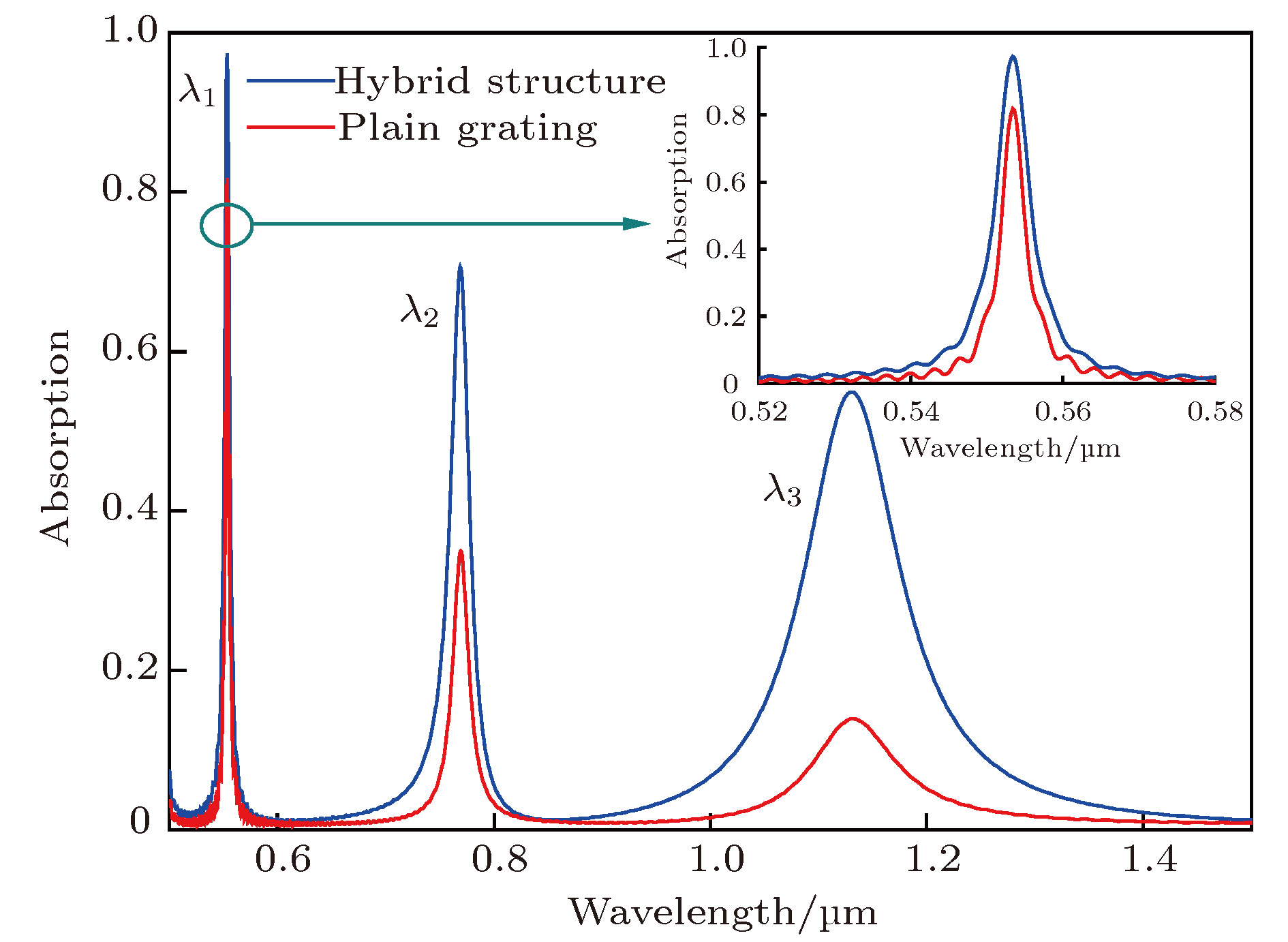
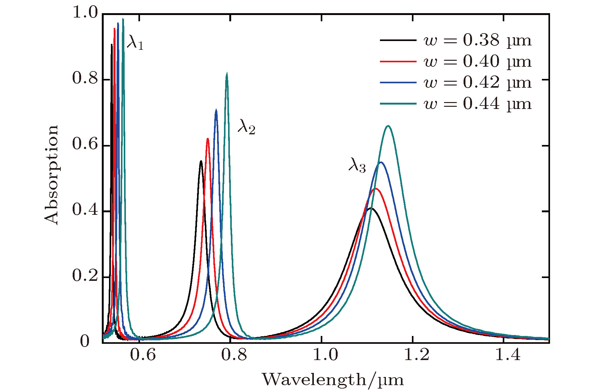
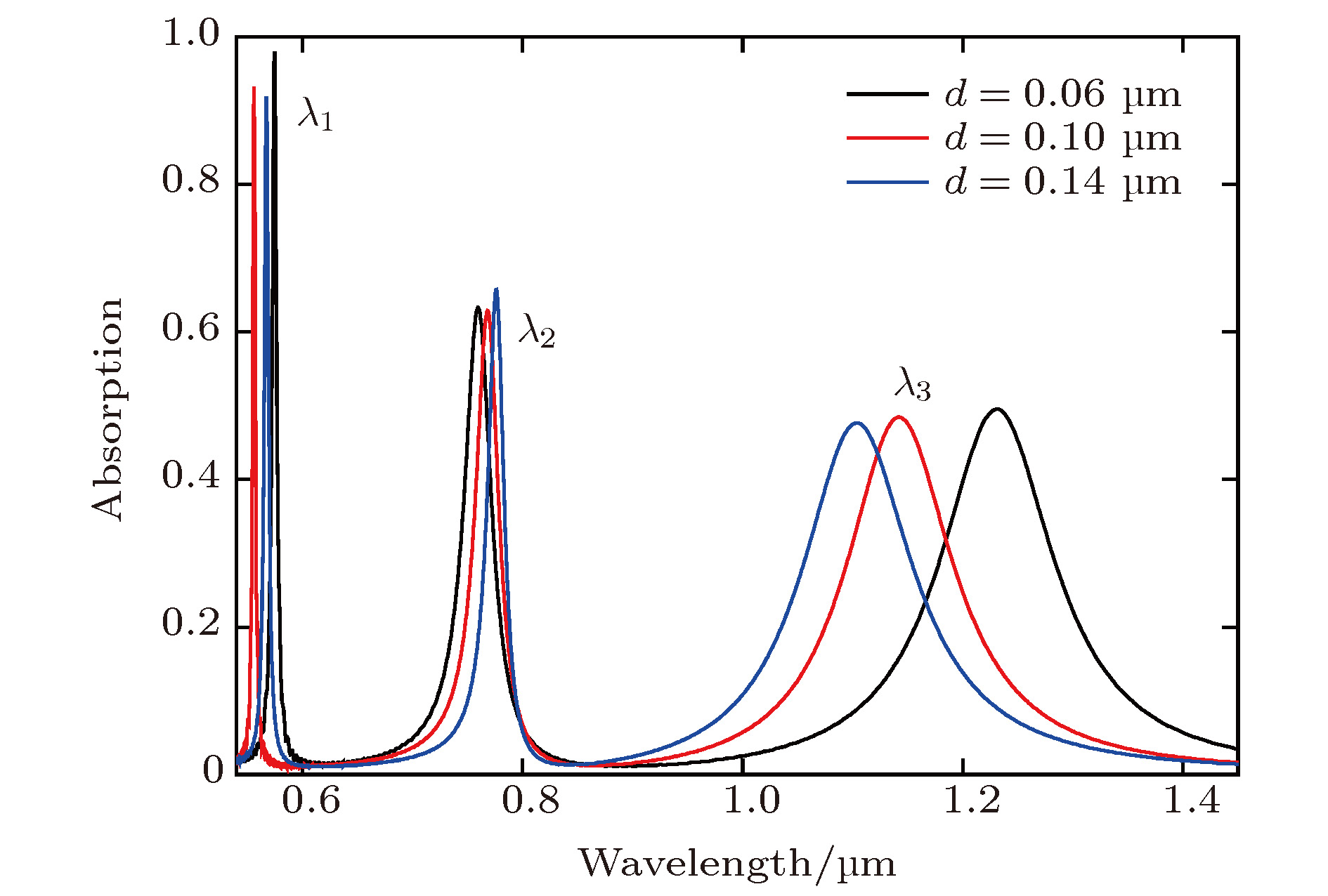
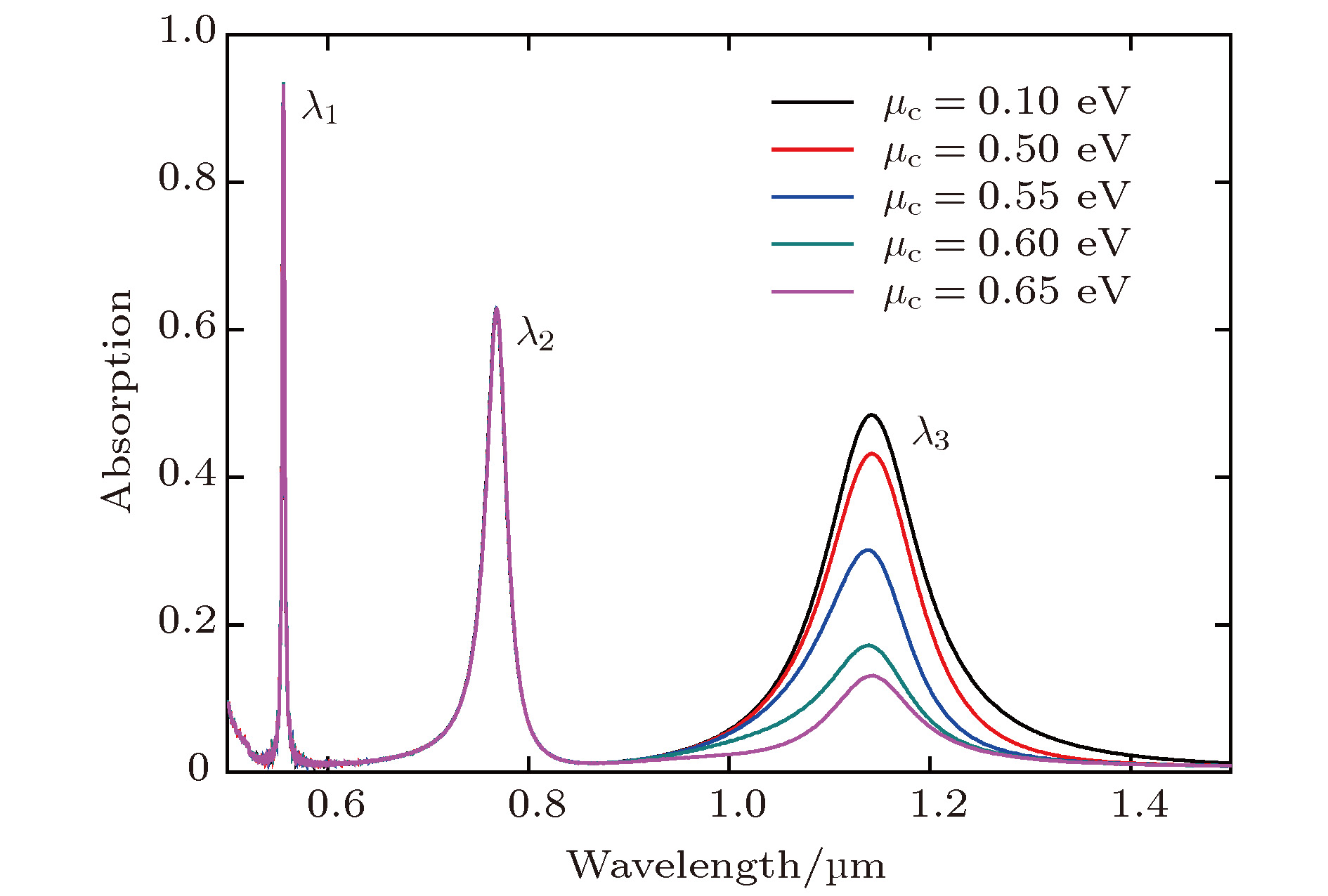
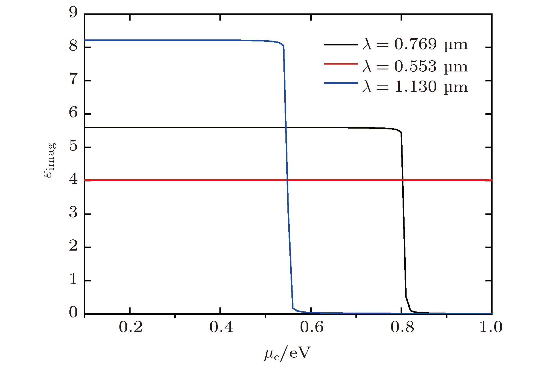
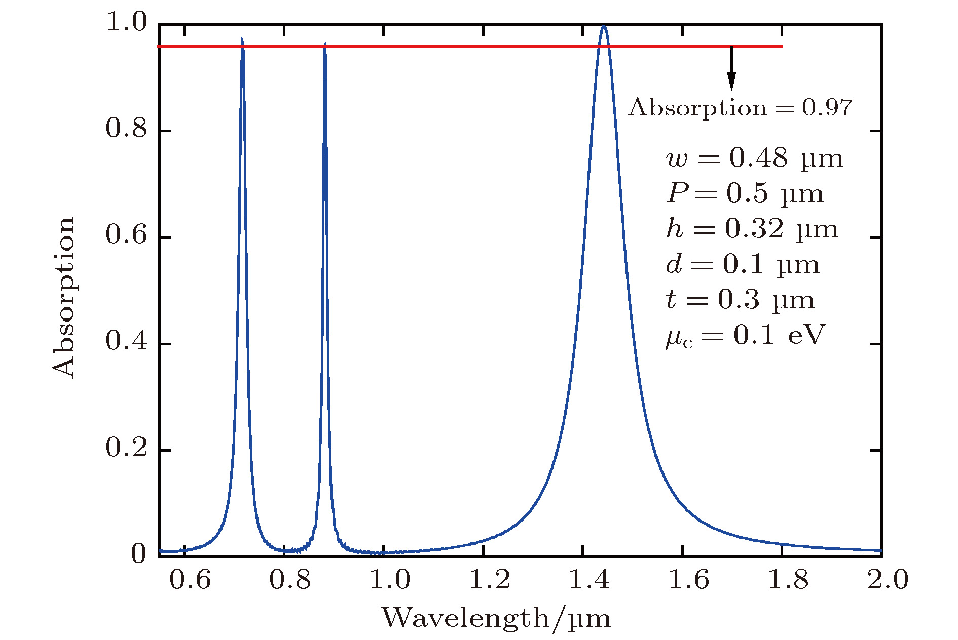
As an emerging new material, graphene has aroused the great research interest. How to improve its absorption efficiency is one of the hot research topics. However, currently most of the studies concentrate in THz band or middle-to-far-infrared region: the research in the visible and near-infrared regions is rare, which greatly limits the applications of graphene in opto-electric fields. In order to improve the absorption efficiency of single-layered graphene in visible and near-infrared band and realize multi-channel optical absorption enhancement, we propose a hybrid structure consisting of graphene-metal grating-dielectric layer-metal substrate. The proposed structure can realize three-channel light absorption enhancement at wavelengths λ1 = 0.553 μm, λ2 = 0.769 μm, and λ3 = 1.130 μm. The maximum absorption efficiency of graphene is 41%, which is 17.82 times that of single-layered graphene. The magnetic field distributions of the hybrid structure at three resonance wavelengths are calculated respectively. It can be found that for the resonance peak λ1, the energy of light field is distributed mainly on the surface of metal grating, which is the characteristic of surface plasmon polariton (SPP) resonance. Therefore, it can be judged that the enhancement of graphene absorption in this channel is due to the SPP resonance stimulated by metal grating. For the resonance peak λ2, the energy of the optical field is mainly confined into the metal grating groove, which is the remarkable resonance characteristic of the Fabry-Pérot (FP) cavity, it can be concluded that the enhancement of the optical absorption of graphene at the resonance peak λ2 is due to the resonance of the FP cavity. When the resonance peak is λ3, the energy of the light field mainly concentrates on the upper and lower edges of the metal grating and permeates into the SiO2 layer, and it can be observed that there are energy concentration points (reddish) at the left end and the right end of the metal grating edge, which is a typical magnetic polariton (MP) resonance feature. Therefore, the enhancement of absorption of graphene at the resonance peak λ3 is caused by the MP resonance induced by the metal grating. We also analyze the absorption characteristic (resonance wavelength and absorption efficiency) dependence on structure parameters by using the finite-difference time-domain (FDTD) simulation. Our study reveals that by increasing grating width, all the three resonance wavelengths are red-shifted, and the absorption efficiency at λ2 and λ3 are both enhanced whereas the absorption efficiency at λ1 almost keeps unchanged. By increasing dielectric layer thickness, λ2 will be red-shifted and λ3 will be blue-shifted, whereas the absorption efficiency at the three resonance wavelengths all remain constant. By increasing graphene chemical potential, none of the wavelengths of the three absorption peaks is shifted, and the absorption efficiency at λ3 decreases. According to our findings, we optimize structure parameters and achieve the light absorption efficiency larger than 97% at the three channels simultaneously, which can make metamaterial absorbers.
[1] Zhao B, Zhao J M, Zhang Z M 2014 Appl. Phys. Lett. 105 031905
[2] Lee C, Wei X, Kysar J W, Hone J 2008 Science 321 385
 Google Scholar
[3] Du X, Skachko I, Barker A, Andrei E Y 2008 Nature Nanotechnol. 3 491
 Google Scholar
[4] 梁振江, 刘海霞, 牛燕雄, 尹贻恒 2016 物理学报 65 138501
 Google Scholar
Liang Z J, Liu H X, Niu Y X, Yin Y H 2016 Acta Phys. Sin. 65 138501
 Google Scholar
[5] Sukosin T, Frank H L K, Javier G D A 2012 Phys. Rev. Lett. 108 47401
 Google Scholar
[6] Zhao Z, Li G, Yu F, Yang H, Chen X, Lu W 2018 Plasmonics 13 2267
[7] 梁振江, 刘海霞, 牛燕雄, 刘凯铭, 尹贻恒 2016 物理学报 65 168101
 Google Scholar
Liang Z J, Liu H X, Niu Y X, Liu K M,Yin Y H 2016 Acta Phys. Sin. 65 168101
 Google Scholar
[8] Gao Y, Zhou G, Zhao N, Tsang H K, Shu C 2018 Opt. Lett. 43 1399
 Google Scholar
[9] Ferrari A, Ferrante C, Virga A, Benfatto L, Martinati M, Fazio D D 2018 Nat. Commun. 9 308
 Google Scholar
[10] Sun Z, Hasan T, Torrisi F, Popa D, Privitera G, Wang F 2010 Acs Nano 4 803
 Google Scholar
[11] Qiu J, Shang Y, Chen X, Li S, Ma W, Wan X 2018 J. Mater. Sci. Technol. 34 2197
[12] Zhang L, Ding Z C, Tong T, Liu J 2017 Nanoscale 9 3524
 Google Scholar
[13] Hsiao T J, Eyassu T, Henderson K, Kim T, Lin C T 2013 Nanotechnology 24 395401
 Google Scholar
[14] Lu H, Cumming B P, Gu M 2015 Opt. Lett. 40 3647
 Google Scholar
[15] Fang Z Y, Wang Y M, Schlather A E, Liu Z, Ajayan P M 2014 Nano Lett. 14 299
 Google Scholar
[16] 张会云, 黄晓燕, 陈琦, 丁春峰, 李彤彤 吕欢欢 徐世林 张晓 张玉萍 姚建铨 2016 物理学报 65 018101
 Google Scholar
Zhang H Y, Huang X Y, Chen Q, Ding C F, Li T T, Lü H H, Xu S L, Zhang X, Zhang Y P, Yao J 2016 Acta Phys. Sin. 65 018101
 Google Scholar
[17] Sang T, Wang R, Li J L, Zhou J Y, Wang Y K 2018 Opt. Commun. 413 255
 Google Scholar
[18] Wang B, Qin C, Huang H, Long H, Wang K, Lu P 2014 Opt. Express 22 25324
 Google Scholar
[19] Nair R R, Blake P, Grigorenko A N, Novoselov K S, Booth T J 2008 Science 320 1308
 Google Scholar
[20] Liu Y, Chadha A, Zhao D, Piper J R 2014 Appl. Phys. Lett. 105 181105
 Google Scholar
[21] Furchi M, Urich A, Pospischil A, Lilley G, Unterrainer K 2012 Nano Lett. 12 2273
[22] Liu J T, Liu N H, Li J, Li X J, Huang J H 2012 Appl. Phys. Lett. 101 052104
 Google Scholar
[23] Zhang L, Tang L, Wei W, Cheng X, Wang W, Zhang H 2016 Opt. Express 24 20002
 Google Scholar
[24] Fang Z, Wang Y, Zheng L, Schlather A, Ajayan P M 2012 Acs Nano 6 10222
 Google Scholar
[25] Xia S X, Zhai X, Huang Y, Liu J Q, Wang L L, Wen S C 2017 Opt. Lett. 42 3052
 Google Scholar
[26] Thareja V, Kang J H, Yuan H, Milaninia K M, Hwang H Y, Cui Y 2015 Nano Lett. 15 1570
 Google Scholar
[27] 高健, 桑田, 李俊浪, 王啦 2018 物理学报 67 184210
 Google Scholar
Gao J, Sang T, Li J L, Wang L 2018 Acta Phys. Sin. 67 184210
 Google Scholar
[28] Liu B, Tang C, Chen J Pei M, Wang Q 2017 Opt. Express 25 12061
 Google Scholar
[29] 陈浩, 张晓霞, 王鸿, 姬月华 2018 物理学报 67 118101
 Google Scholar
Chen H, Zhang X X, Wang H, Ji Y H. 2018 Acta Phys. Sin. 67 118101
 Google Scholar
[30] Bao Q, Zhang H, Wang B, Ni Z, Wang Y 2011 Nature Photo. 5 411
 Google Scholar
[31] Zhao B, Zhao J M, Zhang Z M 2015 J. Opt. Soc. Am. B 32 1176
 Google Scholar
[32] Wang L P, Zhang Z M 2009 Appl. Phys. Lett. 95 111904
 Google Scholar
[33] Garciavidal F J, Sanchezdehesa J, Dechelette A 2002 J. Lightwave Technol. 11 2191
[34] 叶胜威 2018 博士学位论文(成都: 电子科技大学)
[35] Su Z, Yin J, Zhao X 2015 Opt. Express 23 1679
 Google Scholar
[36] Luo C, Ling F, Yao G 2016 Opt. Express 24 1518
 Google Scholar
-
-
[1] Zhao B, Zhao J M, Zhang Z M 2014 Appl. Phys. Lett. 105 031905
[2] Lee C, Wei X, Kysar J W, Hone J 2008 Science 321 385
 Google Scholar
[3] Du X, Skachko I, Barker A, Andrei E Y 2008 Nature Nanotechnol. 3 491
 Google Scholar
[4] 梁振江, 刘海霞, 牛燕雄, 尹贻恒 2016 物理学报 65 138501
 Google Scholar
Liang Z J, Liu H X, Niu Y X, Yin Y H 2016 Acta Phys. Sin. 65 138501
 Google Scholar
[5] Sukosin T, Frank H L K, Javier G D A 2012 Phys. Rev. Lett. 108 47401
 Google Scholar
[6] Zhao Z, Li G, Yu F, Yang H, Chen X, Lu W 2018 Plasmonics 13 2267
[7] 梁振江, 刘海霞, 牛燕雄, 刘凯铭, 尹贻恒 2016 物理学报 65 168101
 Google Scholar
Liang Z J, Liu H X, Niu Y X, Liu K M,Yin Y H 2016 Acta Phys. Sin. 65 168101
 Google Scholar
[8] Gao Y, Zhou G, Zhao N, Tsang H K, Shu C 2018 Opt. Lett. 43 1399
 Google Scholar
[9] Ferrari A, Ferrante C, Virga A, Benfatto L, Martinati M, Fazio D D 2018 Nat. Commun. 9 308
 Google Scholar
[10] Sun Z, Hasan T, Torrisi F, Popa D, Privitera G, Wang F 2010 Acs Nano 4 803
 Google Scholar
[11] Qiu J, Shang Y, Chen X, Li S, Ma W, Wan X 2018 J. Mater. Sci. Technol. 34 2197
[12] Zhang L, Ding Z C, Tong T, Liu J 2017 Nanoscale 9 3524
 Google Scholar
[13] Hsiao T J, Eyassu T, Henderson K, Kim T, Lin C T 2013 Nanotechnology 24 395401
 Google Scholar
[14] Lu H, Cumming B P, Gu M 2015 Opt. Lett. 40 3647
 Google Scholar
[15] Fang Z Y, Wang Y M, Schlather A E, Liu Z, Ajayan P M 2014 Nano Lett. 14 299
 Google Scholar
[16] 张会云, 黄晓燕, 陈琦, 丁春峰, 李彤彤 吕欢欢 徐世林 张晓 张玉萍 姚建铨 2016 物理学报 65 018101
 Google Scholar
Zhang H Y, Huang X Y, Chen Q, Ding C F, Li T T, Lü H H, Xu S L, Zhang X, Zhang Y P, Yao J 2016 Acta Phys. Sin. 65 018101
 Google Scholar
[17] Sang T, Wang R, Li J L, Zhou J Y, Wang Y K 2018 Opt. Commun. 413 255
 Google Scholar
[18] Wang B, Qin C, Huang H, Long H, Wang K, Lu P 2014 Opt. Express 22 25324
 Google Scholar
[19] Nair R R, Blake P, Grigorenko A N, Novoselov K S, Booth T J 2008 Science 320 1308
 Google Scholar
[20] Liu Y, Chadha A, Zhao D, Piper J R 2014 Appl. Phys. Lett. 105 181105
 Google Scholar
[21] Furchi M, Urich A, Pospischil A, Lilley G, Unterrainer K 2012 Nano Lett. 12 2273
[22] Liu J T, Liu N H, Li J, Li X J, Huang J H 2012 Appl. Phys. Lett. 101 052104
 Google Scholar
[23] Zhang L, Tang L, Wei W, Cheng X, Wang W, Zhang H 2016 Opt. Express 24 20002
 Google Scholar
[24] Fang Z, Wang Y, Zheng L, Schlather A, Ajayan P M 2012 Acs Nano 6 10222
 Google Scholar
[25] Xia S X, Zhai X, Huang Y, Liu J Q, Wang L L, Wen S C 2017 Opt. Lett. 42 3052
 Google Scholar
[26] Thareja V, Kang J H, Yuan H, Milaninia K M, Hwang H Y, Cui Y 2015 Nano Lett. 15 1570
 Google Scholar
[27] 高健, 桑田, 李俊浪, 王啦 2018 物理学报 67 184210
 Google Scholar
Gao J, Sang T, Li J L, Wang L 2018 Acta Phys. Sin. 67 184210
 Google Scholar
[28] Liu B, Tang C, Chen J Pei M, Wang Q 2017 Opt. Express 25 12061
 Google Scholar
[29] 陈浩, 张晓霞, 王鸿, 姬月华 2018 物理学报 67 118101
 Google Scholar
Chen H, Zhang X X, Wang H, Ji Y H. 2018 Acta Phys. Sin. 67 118101
 Google Scholar
[30] Bao Q, Zhang H, Wang B, Ni Z, Wang Y 2011 Nature Photo. 5 411
 Google Scholar
[31] Zhao B, Zhao J M, Zhang Z M 2015 J. Opt. Soc. Am. B 32 1176
 Google Scholar
[32] Wang L P, Zhang Z M 2009 Appl. Phys. Lett. 95 111904
 Google Scholar
[33] Garciavidal F J, Sanchezdehesa J, Dechelette A 2002 J. Lightwave Technol. 11 2191
[34] 叶胜威 2018 博士学位论文(成都: 电子科技大学)
[35] Su Z, Yin J, Zhao X 2015 Opt. Express 23 1679
 Google Scholar
[36] Luo C, Ling F, Yao G 2016 Opt. Express 24 1518
 Google Scholar
Catalog
Metrics
- Abstract views: 18461
- PDF Downloads: 150
- Cited By: 0


 DownLoad:
