-
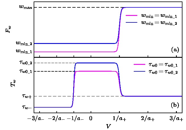
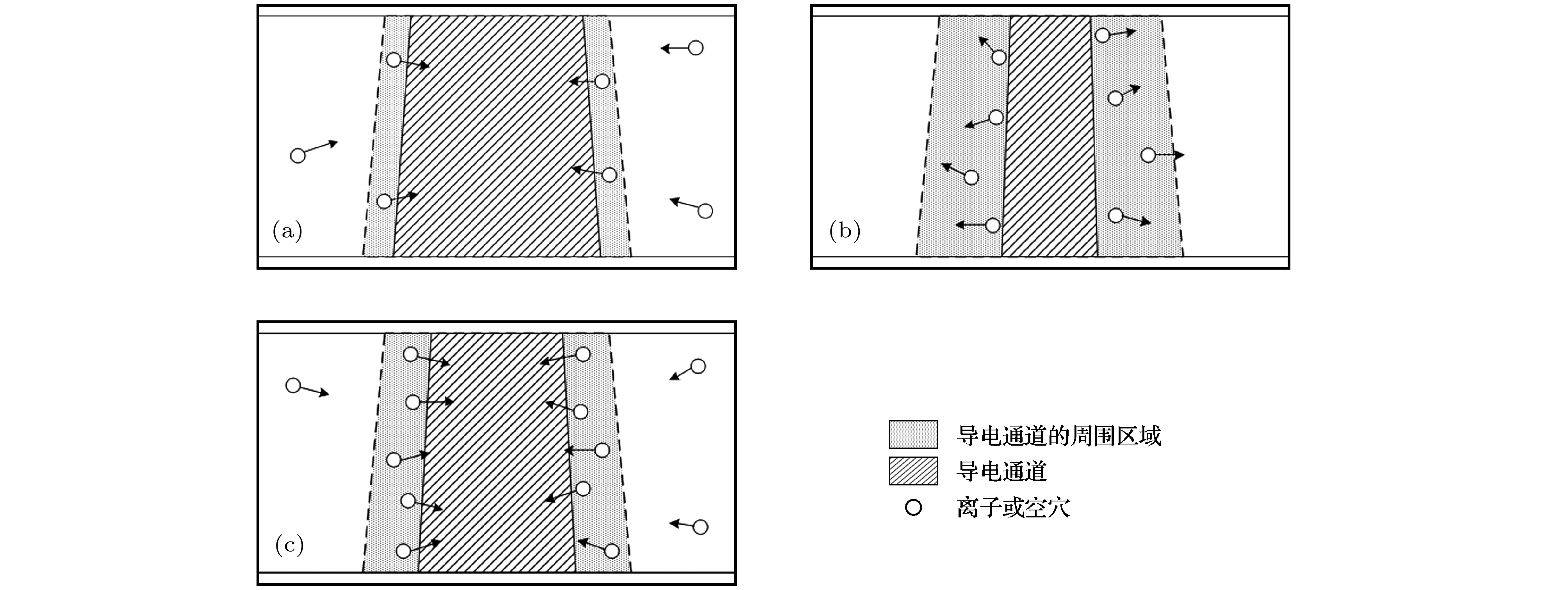
The behavior of transition from short-term memory (STM) to long-term memory (LTM) has been observed and reported in the experimental studies of memristors fabricated by different materials. This kind of memristor in this paper is named STM→LTM memristor. In some of these experimental researches, the learning-experience behavior observed in the " learning-forgetting-relearning” experiment is also reported. When the memristor is restimulated by pulses after forgetting the STM, its memory will quickly return to the highest state that has been reached before the forgetting period, and the memory recovery during the relearning period is obviously faster than the memory formation in the first learning process. In this paper, the behavior of the existing STM→LTM memristor model in the " learning-forgetting-relearning” experiment is further discussed. If wmax, the upper bound of the memory level, is a constant with a value of 1, the STM→LTM memristor model exhibits no learning-experience behavior, and this model shows a faster relearning behavior in the " learning-forgetting-relearning” experiment. The relearning process is faster because the memory forgetting during pulse-to-pulse interval in the relearning process is slower than that in the first learning process. In the STM→LTM memristor model with learning-experience behavior, wmax is redesigned as a state variable in [0,1], and its value will be influenced by the applied voltage. The memory formation in the first learning process is relatively slow because wmax limits the memory formation speed when the pulse is applied. After the forgetting process, the limitation of wmax on the pulse-induced memory formation is less obvious, so the memory of the device increases at a faster speed during the memory recovery of the relearning process. In this case, the forgetting speed still becomes slower after each pulse has been applied. If the pulse-induced wmax increase is so fast that wmax will quickly increase to its upper bound after a few pulses have been applied in the first learning process, and the learning-experience behavior is similar to the faster relearning behavior when wmax = 1. In most of experimental research papers about the STM→LTM memristor, the change of the memristance can be explained by the formation and annihilation of the conductive channel between two electrodes of a memristor. During a certain period of time, the ions (or vacancies), which can be used to form the conductive channel, are only those that are around the conductive channel, which indicates that there should be an upper bound for the size of the conductive channel within this time period. The area in which ions (or vacancies) can be used to form the conductive channel is called the surrounding area of the conductive channel. In the model, wmax can be understood as the size of the conductive channel’s surrounding area, and it describes the upper bound of the width of the conductive channel.
-
Keywords:
- memristor /
- learning-experience behavior /
- short-term memory /
- long-term memory
[1] Chang T, Jo S H, Lu W 2011 ACS Nano 5 7669
 Google Scholar
[2] Yang R, Terabe K, Yao Y P, Tsuruoka T, Hasegawa T, Gimzewski J K, Aono M 2013 Nanotechnology 24 384003
 Google Scholar
[3] Lei Y, Liu Y, Xia Y D, Gao X, Xu B, Wang S D, Yin J, Liu Z G 2014 AIP Adv. 4 077105
 Google Scholar
[4] Xiao Z G, Huang J S 2016 Adv. Electron. Mater. 2 1600100
 Google Scholar
[5] Kim M K, Lee J S 2018 ACS Nano 12 1680
 Google Scholar
[6] Luo W Q, Yuan F Y, Wu H Q, Pan L Y, Deng N, Zeng F, Wei R S, Cai X J 2015 15th Non-Volatile Memory Technology Symposium (NVMTS) Beijing, China, October 12−14, 2015 p7457490
[7] Wang L G, Zhang W, Chen Y, Cao Y Q, Li A D, Wu D 2017 Nanoscale Res. Lett. 12 65
 Google Scholar
[8] La Barbera S, Vuillaume D, Alibart F 2015 ACS Nano 9 941
 Google Scholar
[9] Kim H J, Park D, Yang P, Beom K, Kim M J, Shin C, Kang C J, Yoon T S 2018 Nanotechnology 29 265204
 Google Scholar
[10] Ohno T, Hasegawa T, Tsuruoka T, Terabe K, Gimzewski J K, Aono M 2011 Nat. Mater. 10 591
 Google Scholar
[11] Nayak A, Ohno T, Tsuruoka T, Terabe K, Hasegawa T, Gimzewski J K, Aono M 2012 Adv. Funct. Mater. 22 3606
 Google Scholar
[12] Ohno T, Hasegawa T, Nayak A, Tsuruoka T, Gimzewski J K, Aono M 2011 Appl. Phys. Lett. 99 203108
 Google Scholar
[13] Pan Y, Wan T, Du H, Qu B, Wang D, Ha T J, Chu D 2018 J. Alloys Compd. 757 496
 Google Scholar
[14] Zhou L, Mao J Y, Ren Y, Yang J Q, Zhang S R, Zhou Y, Liao Q, Zeng Y J, Shan H, Xu Z, Fu J, Wang Y, Chen X, Lv Z, Han S T, Roy V A L 2018 Small 14 1800288
 Google Scholar
[15] Liu J, Yang H F, Ji Y, Ma Z Y, Chen K J, Zhang X X, Zhang H, Sun Y, Huang X F, Oda S 2018 Nanotechnology 29 415205
 Google Scholar
[16] Lee T H, Hwang H G, Woo J U, Kim D H, Kim T W, Nahm S 2018 ACS Appl. Mater. Interfaces 10 25673
 Google Scholar
[17] Park Y, Park M J, Lee J S 2018 Adv. Funct. Mater. 28 1804123
 Google Scholar
[18] Lin Y, Zeng T, Xu H Y, Wang Z Q, Zhao X N, Liu W Z, Ma J G, Liu Y C 2018 Adv. Electron. Mater. 4 1800373
 Google Scholar
[19] Wang S P, He C L, Tang J, Yang R, Shi D X, Zhang G Y 2019 Chin. Phys. B 28 017304
 Google Scholar
[20] Mao J Y, Zhou L, Ren Y, Yang J Q, Chang C L, Lin H C, Chou H H, Zhang S R, Zhou Y, Han S T 2019 J. Mater. Chem. C 7 1491
[21] Wang Z Q, Xu H Y, Li X H, Yu H, Liu Y C, Zhu X J 2012 Adv. Funct. Mater. 22 2759
 Google Scholar
[22] Li S Z, Zeng F, Chen C, Liu H Y, Tang G S, Gao S, Song C, Lin Y S, Pan F, Guo D 2013 J. Mater. Chem. C 1 5292
 Google Scholar
[23] Zhang C C, Tai Y T, Shang J, Liu G, Wang K L, Hsu C, Yi X H, Yang X, Xue W H, Tan H W, Guo S S, Pan L, Li R W 2016 J. Mater. Chem. C 4 3217
[24] Park Y, Lee J S 2017 ACS Nano 11 8962
 Google Scholar
[25] Yan X B, Wang J J, Zhao M L, Li X Y, Wang H, Zhang L, Lu C, Ren D L 2018 Appl. Phys. Lett. 113 013503
 Google Scholar
[26] Ren Y, Hu L, Mao J Y, Yuan J, Zeng Y J, Ruan S, Yang J Q, Zhou L, Zhou Y, Han S T 2018 J. Mater. Chem. C 6 9383
 Google Scholar
[27] Liu G, Wang C, Zhang W B, Pan L, Zhang C C, Yang X, Fan F, Chen Y, Li R W 2016 Adv. Electron. Mater. 2 1500298
 Google Scholar
[28] Zhang B, Wang C, Wang L X, Chen Y 2018 J. Mater. Chem. C 6 4023
[29] Li Y, Chu J X, Duan W J, Cai G S, Fan X H, Wang X Z, Wang G, Pei Y L 2018 ACS Appl. Mater. Interfaces 10 24598
 Google Scholar
[30] Zhang S R, Zhou L, Mao J Y, Ren Y, Yang J Q, Yang G H, Zhu X, Han S T, Roy V A L, Zhou Y 2019 Adv. Mater. Technol. 4 1800342
 Google Scholar
[31] Chen L, Li C D, Huang T W, Chen Y R, Wen S P, Qi J T 2013 Phys. Lett. A 377 3260
 Google Scholar
[32] Chen L, Li C D, Huang T W, Hu X F, Chen Y R 2016 Neurocomputing 171 1637
 Google Scholar
[33] 孟凡一, 段书凯, 王丽丹, 胡小方, 董哲康 2015 物理学报 64 148501
 Google Scholar
Meng F Y, Duan S K, Wang L D, Hu X F, Dong Z K 2015 Acta Phys. Sin. 64 148501
 Google Scholar
[34] 邵楠, 张盛兵, 邵舒渊 2016 物理学报 65 128503
 Google Scholar
Shao N, Zhang S B, Shao S Y 2016 Acta Phys. Sin. 65 128503
 Google Scholar
[35] Shao N, Zhang S B, Shao S Y 2017 Chin. Phys. B 26 118501
 Google Scholar
[36] 邵楠, 张盛兵, 邵舒渊 2019 物理学报 68 018501
 Google Scholar
Shao N, Zhang S B, Shao S Y 2019 Acta Phys. Sin. 68 018501
 Google Scholar
[37] Chang T, Jo S H, Kim K H, Sheridan P, Gaba S, Lu W 2011 Appl. Phys. A 102 857
-
图 1 “学习-遗忘-再学习”实验过程的示意说明 (a) 实验各个阶段施加在忆阻器上的电压; (b)−(d) 依次为初次学习过程、遗忘过程、再次学习的记忆恢复过程中忆阻器记忆的变化情况, 横坐标中NL, tf, NR分别表示初次学习的脉冲数量、遗忘过程的时长、再次学习的记忆恢复过程所经历的脉冲数量
Figure 1. Illustration of “learning-forgetting-relearning” experiment: (a) The applied voltage in each period of this experiment; (b)−(d) the change of memristor memory during the first learning process, forgetting process, and the memory recovery period of relearning process, respectively. NL, tf, and NR stand for the number of applied pulses in the first learning process, the forgetting time, and the number of applied pulses in the memory recovery period of the relearning process, respectively.
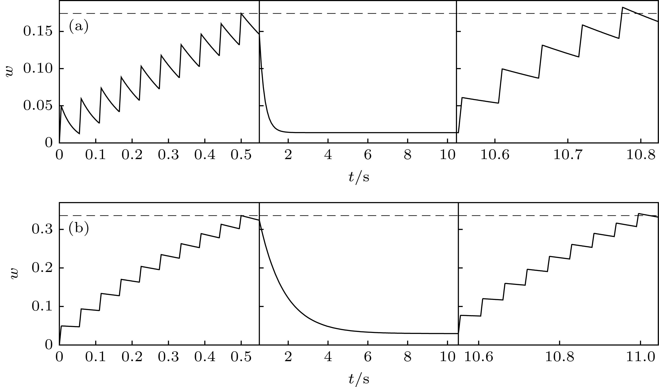
图 3 wmin和τw 0的大小对状态变量w在一个脉冲周期内的变化情况的影响 (a) τw 0 = 0.2 s, wmin取值为不同常数时w的变化情况; (b) wmin = 0.2, τw 0取值为不同常数时w的变化情况
Figure 3. Variation of w within a pulse period when wmin and τw 0 take different values: (a) Variation of w when τw 0 = 0.2 s and wmin takes different values; (b) variation of w when wmin = 0.2 and τw 0 takes different values.
图 4 状态变量τw 0的初值大小对于“学习-遗忘-再学习”过程中w的变化的影响, 虚线标明初次学习阶段w所达到的最大值(a) τw 0初值为0.01 s; (b) τw 0初值为1 s
Figure 4. Influence of the initial value of τw 0 on the variation of w in “learning-forgetting- relearning” process. The maximum value of w during the first learning period is marked by a dashed line: (a) The initial value of τw 0 is 0.01 s; (b) the initial value of τw 0 is 1 s.
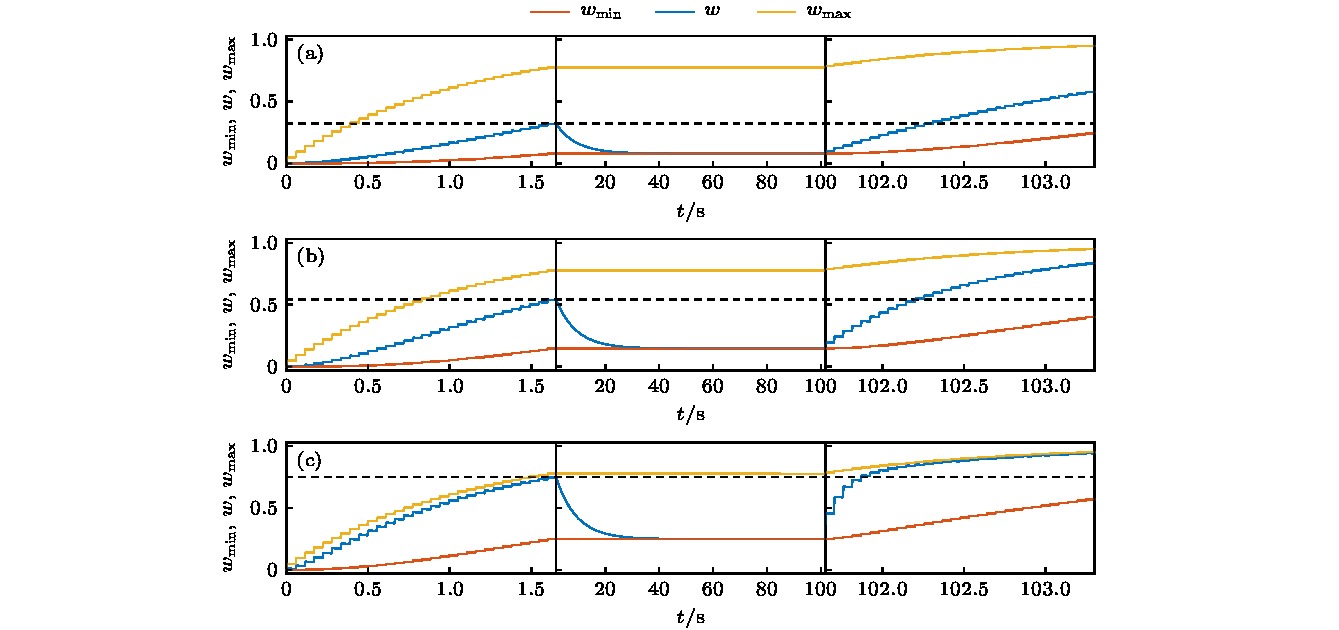
图 5 τw+ = 0.06 s, τmax+ = 0.05 s, τmin+取不同值时的“学习-遗忘-再学习”实验仿真结果 (a) τmin+ = 0.5 s; (b) τmin+ = 0.2 s; (c) τmin+ = 0.1 s. 虚线标出w在初次学习阶段所达到的最大值
Figure 5. Simulations of “learning-forgetting-relearning” process when τw+ = 0.06 s, τmax+ = 0.05 s, and τmin+ takes different values: (a) τmin+ = 0.5 s; (b) τmin+ = 0.2 s; (c) τmin+ = 0.1 s. The maximum value of w during the first learning period is marked by a dashed line.
图 7 τw+ = 0.15 s, τmin+ = 0.1 s, τmax+取不同值时的“学习-遗忘-再学习”实验仿真结果 (a) τmax+ = 0.1 s; (b) τmax+ = 0.05 s; (c) τmax+ = 0.003 s; (d) 当wmax为常数1, 模型其他参数与(a)−(c)相同时的“学习-遗忘-再学习”实验仿真结果. 虚线标出w在初次学习阶段所达到的最大值
Figure 7. Simulations of “learning-forgetting-relearning” process when τw+ = 0.15 s, τmin+ = 0.1 s, and τmax+ takes different values: (a) τmax+ = 0.1 s; (b) τmax+ = 0.05 s; (c) τmax+ = 0.003 s; (d) simulation of “learning-forgetting-relearning” process when wmax = 1, and other parameters are the same as those used in (a)−(c). The maximum value of w during the first learning period is marked by a dashed line.
图 6 τmin+ = 0.2 s, τmax+ = 0.1 s, τw+取不同值时的“学习-遗忘-再学习”实验仿真结果 (a) τw+ = 0.15 s; (b) τw+ = 0.06 s; (c) τw+ = 0.01 s. 虚线标出w在初次学习阶段所达到的最大值
Figure 6. Simulations of “learning-forgetting-relearning” process when τmin+ = 0.2 s, τmax+ = 0.1 s, and τw+ takes different values: (a) τw+ = 0.15 s; (b) τw+ = 0.06 s; (c) τw+ = 0.01 s. The maximum value of w during the first learning period is marked by a dashed line.
图 8 忆阻器两电极间导电通道及其周围区域在“学习-遗忘-再学习”实验中的变化情况 (a) 初次学习阶段; (b) 遗忘阶段; (c) 再次学习的记忆恢复阶段
Figure 8. Change of the conductive channel and its surrounding area during different periods of the “learning-forgetting-relearning” process: (a) The first learning process; (b) the forgetting process; (c) the memory recovery period of the relearning process.
表 1 文献[21—30]中所报道的“学习-遗忘-再学习”实验数据
Table 1. Experimental data of “learning-forgetting-relearning” experiment in References [21—30].
初次学习
脉冲数量记忆遗忘量a) 记忆恢复
脉冲数量文献[21] 80 ~50% 4 文献[22] 50 ~35% 7 文献[23] 80 ~80% 12 文献[24] 50 ~80% 20 文献[25] 30 ~80% 20 文献[26] 50 ~75% 25 文献[27]b) 40 ~60%, ~40% 9, 4 文献[28]b) 40 ~50%, ~40% 16, 6 文献[29]b) 50 ~40%, ~30%, ~29%, ~20% 18, 12, 8 文献[30]b) 50 ~80%, ~55%, ~25% 25, 12, 5 a) “记忆遗忘量”是根据各个文献中所报道的“学习-遗忘-再学习”实验的遗忘曲线, 对于记忆的遗忘量占初次学习所形成的记忆总量的比例给出估计, 各个数据前的“~”表示该数据是根据实验曲线所得的估计值.
b) 在文献[27—30]所报道的实验中经历了多次“遗忘”与“再学习”过程, 表中对这几篇文献依次给出每次遗忘过程的遗忘比例, 以及每次再学习阶段的记忆恢复所经历的脉冲数量. -
[1] Chang T, Jo S H, Lu W 2011 ACS Nano 5 7669
 Google Scholar
[2] Yang R, Terabe K, Yao Y P, Tsuruoka T, Hasegawa T, Gimzewski J K, Aono M 2013 Nanotechnology 24 384003
 Google Scholar
[3] Lei Y, Liu Y, Xia Y D, Gao X, Xu B, Wang S D, Yin J, Liu Z G 2014 AIP Adv. 4 077105
 Google Scholar
[4] Xiao Z G, Huang J S 2016 Adv. Electron. Mater. 2 1600100
 Google Scholar
[5] Kim M K, Lee J S 2018 ACS Nano 12 1680
 Google Scholar
[6] Luo W Q, Yuan F Y, Wu H Q, Pan L Y, Deng N, Zeng F, Wei R S, Cai X J 2015 15th Non-Volatile Memory Technology Symposium (NVMTS) Beijing, China, October 12−14, 2015 p7457490
[7] Wang L G, Zhang W, Chen Y, Cao Y Q, Li A D, Wu D 2017 Nanoscale Res. Lett. 12 65
 Google Scholar
[8] La Barbera S, Vuillaume D, Alibart F 2015 ACS Nano 9 941
 Google Scholar
[9] Kim H J, Park D, Yang P, Beom K, Kim M J, Shin C, Kang C J, Yoon T S 2018 Nanotechnology 29 265204
 Google Scholar
[10] Ohno T, Hasegawa T, Tsuruoka T, Terabe K, Gimzewski J K, Aono M 2011 Nat. Mater. 10 591
 Google Scholar
[11] Nayak A, Ohno T, Tsuruoka T, Terabe K, Hasegawa T, Gimzewski J K, Aono M 2012 Adv. Funct. Mater. 22 3606
 Google Scholar
[12] Ohno T, Hasegawa T, Nayak A, Tsuruoka T, Gimzewski J K, Aono M 2011 Appl. Phys. Lett. 99 203108
 Google Scholar
[13] Pan Y, Wan T, Du H, Qu B, Wang D, Ha T J, Chu D 2018 J. Alloys Compd. 757 496
 Google Scholar
[14] Zhou L, Mao J Y, Ren Y, Yang J Q, Zhang S R, Zhou Y, Liao Q, Zeng Y J, Shan H, Xu Z, Fu J, Wang Y, Chen X, Lv Z, Han S T, Roy V A L 2018 Small 14 1800288
 Google Scholar
[15] Liu J, Yang H F, Ji Y, Ma Z Y, Chen K J, Zhang X X, Zhang H, Sun Y, Huang X F, Oda S 2018 Nanotechnology 29 415205
 Google Scholar
[16] Lee T H, Hwang H G, Woo J U, Kim D H, Kim T W, Nahm S 2018 ACS Appl. Mater. Interfaces 10 25673
 Google Scholar
[17] Park Y, Park M J, Lee J S 2018 Adv. Funct. Mater. 28 1804123
 Google Scholar
[18] Lin Y, Zeng T, Xu H Y, Wang Z Q, Zhao X N, Liu W Z, Ma J G, Liu Y C 2018 Adv. Electron. Mater. 4 1800373
 Google Scholar
[19] Wang S P, He C L, Tang J, Yang R, Shi D X, Zhang G Y 2019 Chin. Phys. B 28 017304
 Google Scholar
[20] Mao J Y, Zhou L, Ren Y, Yang J Q, Chang C L, Lin H C, Chou H H, Zhang S R, Zhou Y, Han S T 2019 J. Mater. Chem. C 7 1491
[21] Wang Z Q, Xu H Y, Li X H, Yu H, Liu Y C, Zhu X J 2012 Adv. Funct. Mater. 22 2759
 Google Scholar
[22] Li S Z, Zeng F, Chen C, Liu H Y, Tang G S, Gao S, Song C, Lin Y S, Pan F, Guo D 2013 J. Mater. Chem. C 1 5292
 Google Scholar
[23] Zhang C C, Tai Y T, Shang J, Liu G, Wang K L, Hsu C, Yi X H, Yang X, Xue W H, Tan H W, Guo S S, Pan L, Li R W 2016 J. Mater. Chem. C 4 3217
[24] Park Y, Lee J S 2017 ACS Nano 11 8962
 Google Scholar
[25] Yan X B, Wang J J, Zhao M L, Li X Y, Wang H, Zhang L, Lu C, Ren D L 2018 Appl. Phys. Lett. 113 013503
 Google Scholar
[26] Ren Y, Hu L, Mao J Y, Yuan J, Zeng Y J, Ruan S, Yang J Q, Zhou L, Zhou Y, Han S T 2018 J. Mater. Chem. C 6 9383
 Google Scholar
[27] Liu G, Wang C, Zhang W B, Pan L, Zhang C C, Yang X, Fan F, Chen Y, Li R W 2016 Adv. Electron. Mater. 2 1500298
 Google Scholar
[28] Zhang B, Wang C, Wang L X, Chen Y 2018 J. Mater. Chem. C 6 4023
[29] Li Y, Chu J X, Duan W J, Cai G S, Fan X H, Wang X Z, Wang G, Pei Y L 2018 ACS Appl. Mater. Interfaces 10 24598
 Google Scholar
[30] Zhang S R, Zhou L, Mao J Y, Ren Y, Yang J Q, Yang G H, Zhu X, Han S T, Roy V A L, Zhou Y 2019 Adv. Mater. Technol. 4 1800342
 Google Scholar
[31] Chen L, Li C D, Huang T W, Chen Y R, Wen S P, Qi J T 2013 Phys. Lett. A 377 3260
 Google Scholar
[32] Chen L, Li C D, Huang T W, Hu X F, Chen Y R 2016 Neurocomputing 171 1637
 Google Scholar
[33] 孟凡一, 段书凯, 王丽丹, 胡小方, 董哲康 2015 物理学报 64 148501
 Google Scholar
Meng F Y, Duan S K, Wang L D, Hu X F, Dong Z K 2015 Acta Phys. Sin. 64 148501
 Google Scholar
[34] 邵楠, 张盛兵, 邵舒渊 2016 物理学报 65 128503
 Google Scholar
Shao N, Zhang S B, Shao S Y 2016 Acta Phys. Sin. 65 128503
 Google Scholar
[35] Shao N, Zhang S B, Shao S Y 2017 Chin. Phys. B 26 118501
 Google Scholar
[36] 邵楠, 张盛兵, 邵舒渊 2019 物理学报 68 018501
 Google Scholar
Shao N, Zhang S B, Shao S Y 2019 Acta Phys. Sin. 68 018501
 Google Scholar
[37] Chang T, Jo S H, Kim K H, Sheridan P, Gaba S, Lu W 2011 Appl. Phys. A 102 857
Catalog
Metrics
- Abstract views: 14514
- PDF Downloads: 163
- Cited By: 0


 DownLoad:


