


-
The memristors and the energy storage capacitors have the same sandwich structure, but the operating voltages required by the two devices are significantly different. Therefore, in the same device, it is necessary to study the influencing factors of operating voltage and adjust the operating voltage of the devices to realize the applications of the device in diverse fields. The polycrystalline ZrO2 and amorphous TaOx thin films are deposited on ITO conductive glass and Pt/Si substrates by reactive magnetron sputtering technology. Au, Ag and Al metal materials are selected as the top electrodes to construct a variety of metal/insulator/metal sandwich capacitors. The breakdown strengths of these devices under different bias polarities are studied. The results demonstrate that the breakdown strength is slightly larger for the ZrO2 based capacitor with ITO as the bottom electrode than for the Pt electrode device under negative bias. The breakdown electric field of the device with Ag as the top electrode shows obvious dependence on bias polarity, no matter whether the bottom electrode is ITO or Pt. The breakdown strength is reduced by more than an order of magnitude under a positive bias (2.13 MV/cm) compared with under a negative bias (0.17 MV/cm) of Ag/ZrO2/ITO device. The breakdown strength of the Al/TaOx/Pt device is enhanced under the forward bias (3.6 MV/cm), contrary to the Ag electrode device, which is nearly twice higher than the breakdown electric field under the negative bias (1.81 MV/cm). The different breakdown behaviors of the above devices can be explained by the migration and rearrangement of oxygen between the oxide electrode and the dielectric interface layer; the dissolution, migration and reduction of the electrochemically active metal electrode; and the redox reaction between the chemically active metal electrode and the oxide dielectric interface. The ZrO2 based capacitor with ITO electrode undergoes a redox reaction of Sn4+ in the ITO under negative bias, forming an insulating layer at the interface between the dielectric layer and the ITO electrode, which contributes a larger breakdown electric field. In addition, the electrochemical metallization process happens to the Ag electrode device under positive bias, and the breakdown electric field is smaller than negative bias due to the large diffusion coefficient of Ag ions in the film, while breakdown is dominated by the defect characteristics of the dielectric film under negative bias. The Al/TaOx/Pt devices can form AlOx oxide layer under positive bias, spontaneously, which can inhibit the leakage current, and also act as a series resistance to disperse part of the voltage and enhance the breakdown voltage of the device. The experimental results have guided significance in designing and operating the devices with different operating voltage requirements, such as memristors and dielectric energy storage capacitors. -
Keywords:
- oxide films /
- electrode materials /
- bias polarity /
- breakdown mechanism /
- memristors /
- capacitors
[1] Chua L 1971 IEEE Trans. Circuit Theory 18 507
 Google Scholar
[2] Hao X 2013 J. Adv. Dielectr. 3 1330001
Google Scholar
[3] Palneedi H, Peddigari M, Hwang G T, Jeong D Y, Ryu J 2018 Adv. Funct. Mater. 28 1803665
Google Scholar
[4] Zheng T, Wu J, Xiao D, Zhu J 2018 Prog. Mater Sci. 98 552
Google Scholar
[5] Wang Y, Jie W, Yang C, Wei X, Hao J 2019 Adv. Funct. Mater. 29 1808118
Google Scholar
[6] Wang Y, Hu L, Wei X, Zhuge F 2020 Appl. Phys. Lett. 116 221602
Google Scholar
[7] Choi J, Park S, Lee J, Hong K, Kim D H, Moon C W, Park G D, Suh J, Hwang J, Kim S Y, Jung H S, Park N G, Han S, Nam K T, Jang H W 2016 Adv. Mater. 28 6562
Google Scholar
[8] Hu L, Fu S, Chen Y, Cao H, Liang L, Zhang H, Gao J, Wang J, Zhuge F 2017 Adv. Mater. 29 1606927
Google Scholar
[9] Guo J, Wang L, Liu Y, Zhao Z, Zhu E, Lin Z, Wang P, Jia C, Yang S, Lee S J, Huang W, Huang Y, Duan X 2020 Matter 2 965
Google Scholar
[10] Guo X, Wang Q, Lü X, Yang H, Sun K, Yang D, Zhang H, Hasegawa T, He D 2020 Nanoscale 12 4320
Google Scholar
[11] Liu Y, Ye C, Chang K C, Li L, Jiang B, Xia C, Liu L, Zhang X, Liu X, Xia T, Peng Z, Cao G, Cheng G, Ke S, Wang J 2020 Small 16 2004619
Google Scholar
[12] McPherson J W, Jinyoung K, Shanware A, Mogul H, Rodriguez J 2003 IEEE Trans. Electron Devices 50 1771
Google Scholar
[13] Yang L, Kong X, Li F, Hao H, Cheng Z, Liu H, Li J F, Zhang S 2019 Prog. Mater Sci. 102 72
Google Scholar
[14] Pan F, Gao S, Chen C, Song C, Zeng F 2014 Mater. Sci. Eng. R. 83 1
Google Scholar
[15] 庞华, 邓宁 2014 物理学报 63 147301
Google Scholar
Pang H, Deng N 2014 Acta Phys. Sin. 63 147301
Google Scholar
[16] Liu Q, Sun J, Lü H, Long S, Yin K, Wan N, Li Y, Sun L, Liu M 2012 Adv. Mater. 24 1844
Google Scholar
[17] Liu S, Lu N, Zhao X, Xu H, Banerjee W, Lü H, Long S, Li Q, Liu Q, Liu M 2016 Adv. Mater. 28 10623
Google Scholar
[18] Li Q, Qiu L, Wei X, Dai B, Zeng H 2016 Sci. Rep. 6 29347
Google Scholar
[19] Tian B, Nukala P, Hassine M B, Zhao X, Wang X, Shen H, Wang J, Sun S, Lin T, Sun J, Ge J, Huang R, Duan C, Reiss T, Varela M, Dkhil B, Meng X, Chu J 2017 Phys. Chem. Chem. Phys. 19 16960
Google Scholar
[20] Gao W, Yao M, Yao X 2017 Ceram. Int. 43 13069
Google Scholar
[21] Gao W, Yao M, Yao X 2018 ACS Appl. Mater. Interfaces 10 28745
Google Scholar
[22] Hou C, Huang W, Zhao W, Zhang D, Yin Y, Li X 2017 ACS Appl. Mater. Interfaces 9 20484
Google Scholar
[23] Panda D, Tseng T Y 2013 Thin Solid Films 531 1
Google Scholar
[24] Kudoh Y, Akami K, Matsuya Y 1999 Synth. Met. 102 973
Google Scholar
[25] Matsuhashi H, Nishikawa S 1994 Jpn. J. Appl. Phys. 33 1293
Google Scholar
[26] Atanassova E, Paskaleva A 2007 Microelectron. Reliab. 47 913
Google Scholar
[27] Lee M J, Lee C B, Lee D, Lee S R, Chang M, Hur J H, Kim Y B, Kim C J, Seo D H, Seo S, Chung U I, Yoo I K, Kim K 2011 Nat. Mater. 10 625
Google Scholar
[28] Wu M C, Wu T H, Tseng T Y 2012 J. Appl. Phys. 111 014505
Google Scholar
[29] Liu Q, Long S, Wang W, Tanachutiwat S, Li Y, Wang Q, Zhang M, Huo Z, Chen J, Liu M 2010 IEEE Electron Device Lett. 31 1299
Google Scholar
[30] Li Y, Long S, Zhang M, Liu Q, Shao L, Zhang S, Wang Y, Zuo Q, Liu S, Liu M 2009 IEEE Electron Device Lett. 31 117
Google Scholar
[31] Li C, Wang F, Zhang J, She Y, Zhang Z, Liu L, Liu Q, Hao Y, Zhang K 2020 ECS J. Solid State Sci. Technol 9 041005
Google Scholar
[32] Atanassova E, Spassov D, Paskaleva A 2006 Microelectron. Eng. 83 1918
Google Scholar
[33] Kindsmüller A, Meledin A, Mayer J, Waser R, Wouters D J 2019 Nanoscale 11 18201
Google Scholar
[34] Yuan X C, Tang J L, Zeng H Z, Wei X H 2014 Nanoscale Res. Lett. 9 268
Google Scholar
[35] Ye C, Zhan C, Tsai T M, Chang K C, Chen M C, Chang T C, Deng T, Wang H 2014 Appl. Phys. Express 7 034101
Google Scholar
[36] Zhang J, Wang F, Li C, Shan X, Liang A, Hu K, Li Y, Liu Q, Hao Y, Zhang K 2020 Appl. Surf. Sci. 526 146723
Google Scholar
[37] Wu M C, Ting Y H, Chen J Y, Wu W W 2019 Adv. Sci. 6 1902363
Google Scholar
[38] Kuo C C, Chen I C, Shih C C, Chang K C, Huang C H, Chen P H, Chang T, Tsai T M, Chang J S, Huang J C 2015 IEEE Electron Device Lett. 36 1321
Google Scholar
-

图 1 MIM器件用于阻变及储能电容器时的机理图以及对工作电压的要求
Figure 1. Schematic diagram of the MIM devices for resistive switching and energy storage with different operation voltages.

图 2 ZrO2和TaOx薄膜的XRD, AFM和SEM图 (a) ITO基底上沉积的ZrO2薄膜; (b) Pt/Si基底上沉积的ZrO2薄膜; (c) Pt/Si 基底上沉积的TaOx薄膜
Figure 2. XRD, AFM and SEM patterns of the ZrO2 and TaOx thin films: (a) The ZrO2 thin film deposited on ITO/glass; (b) the ZrO2 thin film deposited on Pt/Si; (c) the TaOx thin film deposited on Pt/Si.
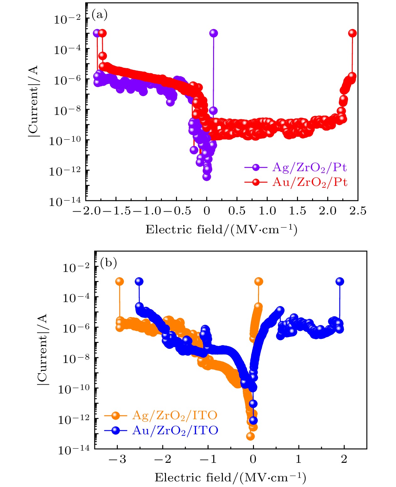
图 3 ZrO2基电容器的I-E特征曲线 (a) Ag/ZrO2/Pt和Au/ZrO2/Pt器件; (b) Ag/ZrO2/ITO和Au/ZrO2/ITO器件
Figure 3. I-E characteristics of ZrO2 based capacitors: (a) Ag/ZrO2/Pt and Au/ZrO2/Pt; (b) Ag/ZrO2/ITO and Au/ZrO2/ITO.

图 4 ZrO2基电容器在正负偏压下的击穿电场统计图
Figure 4. Statistical charts of positive and negative breakdown electric field of ZrO2-based capacitors.
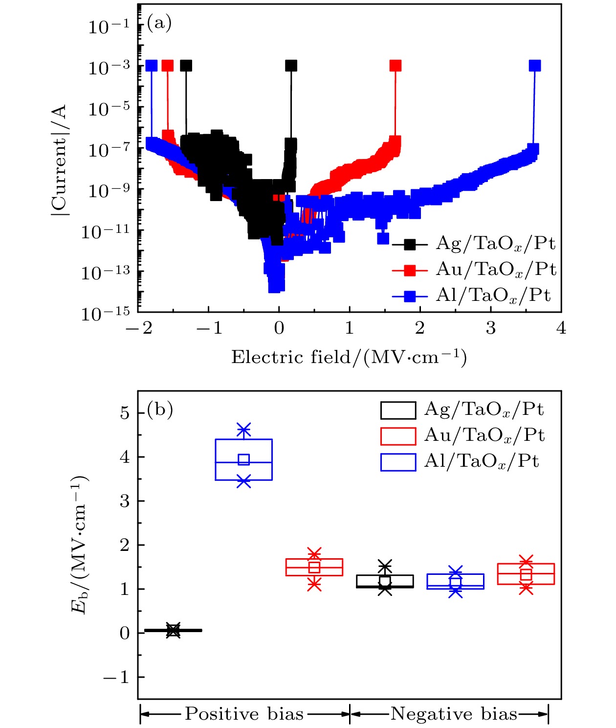
图 5 Pt/Si基底上TaOx基器件 (a) I-E特征曲线; (b)正负偏压下击穿电场值统计图
Figure 5. Positive and negative breakdown electric field of TaOx based devices: (a) I-E characteristics; (b) statistical charts.
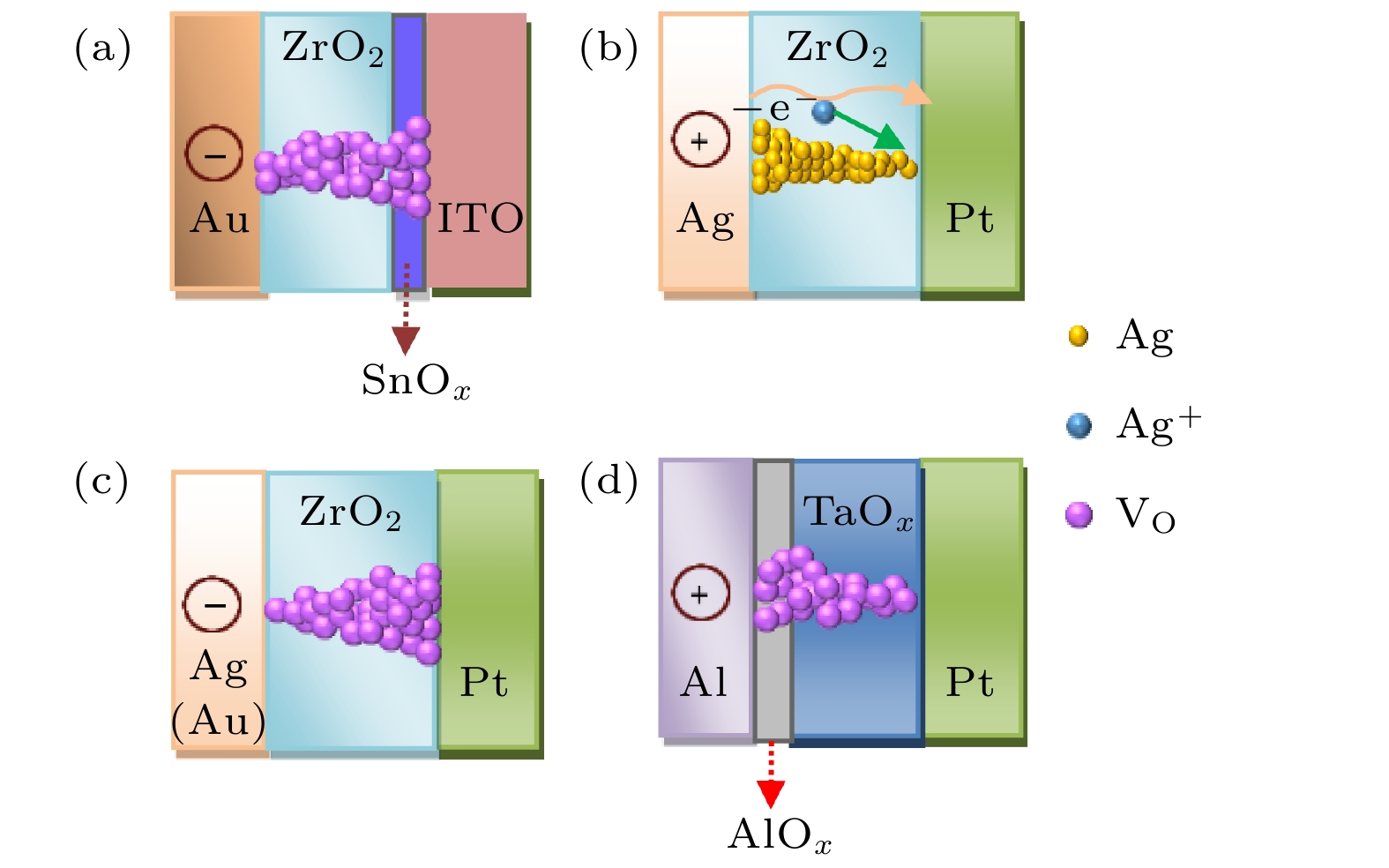
图 6 器件在施加偏压下的击穿机理示意图 (a)负偏压下的Au/ZrO2/ITO器件; (b), (c) 正负偏压下的Ag/ZrO2/Pt器件; (d) 正偏压下的Al/TaOx/Pt器件
Figure 6. Schematic diagrams of the breakdown mechanisms of the devices under different applied biases: (a) The Au/ZrO2/ITO device under negative bias; (b), (c) Ag/ZrO2/Pt devices under positive and negative biases, respectively; (d) the Al/TaOx/Pt device under positive bias.
-
[1] Chua L 1971 IEEE Trans. Circuit Theory 18 507
Google Scholar
[2] Hao X 2013 J. Adv. Dielectr. 3 1330001
Google Scholar
[3] Palneedi H, Peddigari M, Hwang G T, Jeong D Y, Ryu J 2018 Adv. Funct. Mater. 28 1803665
Google Scholar
[4] Zheng T, Wu J, Xiao D, Zhu J 2018 Prog. Mater Sci. 98 552
Google Scholar
[5] Wang Y, Jie W, Yang C, Wei X, Hao J 2019 Adv. Funct. Mater. 29 1808118
Google Scholar
[6] Wang Y, Hu L, Wei X, Zhuge F 2020 Appl. Phys. Lett. 116 221602
Google Scholar
[7] Choi J, Park S, Lee J, Hong K, Kim D H, Moon C W, Park G D, Suh J, Hwang J, Kim S Y, Jung H S, Park N G, Han S, Nam K T, Jang H W 2016 Adv. Mater. 28 6562
Google Scholar
[8] Hu L, Fu S, Chen Y, Cao H, Liang L, Zhang H, Gao J, Wang J, Zhuge F 2017 Adv. Mater. 29 1606927
Google Scholar
[9] Guo J, Wang L, Liu Y, Zhao Z, Zhu E, Lin Z, Wang P, Jia C, Yang S, Lee S J, Huang W, Huang Y, Duan X 2020 Matter 2 965
Google Scholar
[10] Guo X, Wang Q, Lü X, Yang H, Sun K, Yang D, Zhang H, Hasegawa T, He D 2020 Nanoscale 12 4320
Google Scholar
[11] Liu Y, Ye C, Chang K C, Li L, Jiang B, Xia C, Liu L, Zhang X, Liu X, Xia T, Peng Z, Cao G, Cheng G, Ke S, Wang J 2020 Small 16 2004619
Google Scholar
[12] McPherson J W, Jinyoung K, Shanware A, Mogul H, Rodriguez J 2003 IEEE Trans. Electron Devices 50 1771
Google Scholar
[13] Yang L, Kong X, Li F, Hao H, Cheng Z, Liu H, Li J F, Zhang S 2019 Prog. Mater Sci. 102 72
Google Scholar
[14] Pan F, Gao S, Chen C, Song C, Zeng F 2014 Mater. Sci. Eng. R. 83 1
Google Scholar
[15] 庞华, 邓宁 2014 物理学报 63 147301
Google Scholar
Pang H, Deng N 2014 Acta Phys. Sin. 63 147301
Google Scholar
[16] Liu Q, Sun J, Lü H, Long S, Yin K, Wan N, Li Y, Sun L, Liu M 2012 Adv. Mater. 24 1844
Google Scholar
[17] Liu S, Lu N, Zhao X, Xu H, Banerjee W, Lü H, Long S, Li Q, Liu Q, Liu M 2016 Adv. Mater. 28 10623
Google Scholar
[18] Li Q, Qiu L, Wei X, Dai B, Zeng H 2016 Sci. Rep. 6 29347
Google Scholar
[19] Tian B, Nukala P, Hassine M B, Zhao X, Wang X, Shen H, Wang J, Sun S, Lin T, Sun J, Ge J, Huang R, Duan C, Reiss T, Varela M, Dkhil B, Meng X, Chu J 2017 Phys. Chem. Chem. Phys. 19 16960
Google Scholar
[20] Gao W, Yao M, Yao X 2017 Ceram. Int. 43 13069
Google Scholar
[21] Gao W, Yao M, Yao X 2018 ACS Appl. Mater. Interfaces 10 28745
Google Scholar
[22] Hou C, Huang W, Zhao W, Zhang D, Yin Y, Li X 2017 ACS Appl. Mater. Interfaces 9 20484
Google Scholar
[23] Panda D, Tseng T Y 2013 Thin Solid Films 531 1
Google Scholar
[24] Kudoh Y, Akami K, Matsuya Y 1999 Synth. Met. 102 973
Google Scholar
[25] Matsuhashi H, Nishikawa S 1994 Jpn. J. Appl. Phys. 33 1293
Google Scholar
[26] Atanassova E, Paskaleva A 2007 Microelectron. Reliab. 47 913
Google Scholar
[27] Lee M J, Lee C B, Lee D, Lee S R, Chang M, Hur J H, Kim Y B, Kim C J, Seo D H, Seo S, Chung U I, Yoo I K, Kim K 2011 Nat. Mater. 10 625
Google Scholar
[28] Wu M C, Wu T H, Tseng T Y 2012 J. Appl. Phys. 111 014505
Google Scholar
[29] Liu Q, Long S, Wang W, Tanachutiwat S, Li Y, Wang Q, Zhang M, Huo Z, Chen J, Liu M 2010 IEEE Electron Device Lett. 31 1299
Google Scholar
[30] Li Y, Long S, Zhang M, Liu Q, Shao L, Zhang S, Wang Y, Zuo Q, Liu S, Liu M 2009 IEEE Electron Device Lett. 31 117
Google Scholar
[31] Li C, Wang F, Zhang J, She Y, Zhang Z, Liu L, Liu Q, Hao Y, Zhang K 2020 ECS J. Solid State Sci. Technol 9 041005
Google Scholar
[32] Atanassova E, Spassov D, Paskaleva A 2006 Microelectron. Eng. 83 1918
Google Scholar
[33] Kindsmüller A, Meledin A, Mayer J, Waser R, Wouters D J 2019 Nanoscale 11 18201
Google Scholar
[34] Yuan X C, Tang J L, Zeng H Z, Wei X H 2014 Nanoscale Res. Lett. 9 268
Google Scholar
[35] Ye C, Zhan C, Tsai T M, Chang K C, Chen M C, Chang T C, Deng T, Wang H 2014 Appl. Phys. Express 7 034101
Google Scholar
[36] Zhang J, Wang F, Li C, Shan X, Liang A, Hu K, Li Y, Liu Q, Hao Y, Zhang K 2020 Appl. Surf. Sci. 526 146723
Google Scholar
[37] Wu M C, Ting Y H, Chen J Y, Wu W W 2019 Adv. Sci. 6 1902363
Google Scholar
[38] Kuo C C, Chen I C, Shih C C, Chang K C, Huang C H, Chen P H, Chang T, Tsai T M, Chang J S, Huang J C 2015 IEEE Electron Device Lett. 36 1321
Google Scholar

 DownLoad:
Catalog
Metrics
- Abstract views: 8723
- PDF Downloads: 124
- Cited By: 0
