-
Multi-wavelength confocal lens is an indispensable part of optical system, the traditional optical confocal system is often added by a certain number of optical lenses, or uses a different combination of optical lenses of different materials to implement multi-wavelength co-focusing,making the system possess a larger volume and weight, which, however, is difficult to meet the requirements for high integration and miniaturization of the system. As an optical element composed of two-dimensional planar subwavelength micro-element structure, the metalens has the advantages of flatness, ultra-thinness and regulating light waves, and has great potential applications in highly integrated and miniaturized optical confocal systems. According to relevant research reports, it is known that the existing research schemes of multi-wavelength confocal metalens have some shortcomings, such as relatively complex structure and relatively low focusing efficiency. In this work, a kind of metalens composed of simple micro-element structure is proposed and designed, which can simultaneously realize the long infrared dual wavelength confocal function. Based on the generalized Snell's law and the transmission phase modulation mechanism, a scientific evaluation function is established to select the optimal array of micro-elements structure to form a metalens. With the elliptical nano silicon column in a simple micro-element structure, the wavefront phase of the long infrared dual wavelength in the orthogonal linear polarization state can be adjusted independently and efficiently , while reducing the wavelength crosstalk and improving the focusing efficiency. The design results show that the proposed metalens achieves dual wavelength co-focused with a wavelength of 10.6 and 9.3 μm, and has a high focusing efficiency, The focusing spot is close to the diffraction limit. The quantitative analysis of the redundancy of the structural parameters of the metalens micro-element structure is made, and the trend of its influence on the focusing efficiency and the allowable deviation range of the micro-element structure parameters are obtained, which provides a theoretical basis for further precisely controlling the device fabrication. The matalens designed in this work is expected to meet the requirements for integration and miniaturization of long infrared optical confocal system, and has important applications in laser surgery, industrial cutting and welding and other fields.
-
Keywords:
- metalens /
- confocal /
- double wavelength
[1] Vitruk P 2017 Dental Town 17 62
[2] Linden E, Vitruk P 2015 Implant Pract. 8 30
[3] Bhadra R, Biswas P, Sankar M R 2015 Lasers based manufacturing (New Delhi: Springer) pp381–398
[4] Khorasaninejad M, Capasso F 2017 Science 358 1146
 Google Scholar
[5] Lalanne P, Chavel P 2017 Laser Photonics Rev. 11 1600295
 Google Scholar
[6] Ming L T, Hsiao H H, Cheng H C, Mu K C, Sun G, & Liu A Q, Tsai D P 2018 Adv. Opt. Mater. 6 1800554
 Google Scholar
[7] Chen M K, Wu Y, Feng L, Fan Q, Lu M, Xu T, Tsai D P 2021 Adv. Opt. Mater. 9 2001414
 Google Scholar
[8] Banerji S, Meem M, Sensale-Rodriguez B, Majμmder A, Vasquez F G, Menon R 2019 Optica 6 805
 Google Scholar
[9] Zou X, Zheng G, Yuan Q, Zang W, Zhu S 2020 Photoni X 1 2
 Google Scholar
[10] Chen W T, Zhu A Y, Capasso F 2020 Nat. Rev. Mater. 5 604
 Google Scholar
[11] Aieta F, Kats M A, Genevet P, Capasso F 2015 Science 347 1342
 Google Scholar
[12] Khorasaninejad M, Aieta F, Kanhaiya P, Kats M A, Genevet P, Rousso D, Capasso F 2015 Nano Lett. 15 5358
 Google Scholar
[13] Genevet P, Capasso F, Aieta F, Khorasaninejad M, Devlin R 2017 Optica 4 139
 Google Scholar
[14] Arbabi E, Arbabi A, Kamali S M, Horie Y, Faraon A 2016 Optica 3 628
 Google Scholar
[15] Lin D, Holsteen A L, Maguid E, Wetzstein G, Kik P G, Hasman E, Brongersma M L 2016 Nano Lett. 16 7671
 Google Scholar
[16] Arbabi E, Arbabi A, Kamali S M, Horie Y, Faraon A 2016 Sci. Rep. 6 32803
 Google Scholar
[17] Avayu O, Almeida E, Prior Y, Ellenbogen T 2017 Nat. Commun. 8 14992
 Google Scholar
[18] Yang H, Li G, Cao G, Yu F, Zhao Z, Ou K, Chen X, Lu Wei 2018 Opt. Mater. Express 8 1940
 Google Scholar
[19] Fan Q, Liu M, Yang C, Yu L, Yan F, Xu T 2018 Appl. Phys. Lett. 113 01104
[20] Fan Q, Wang Y, Liu M, Xu T 2018 Opt. Lett. 43 6005
 Google Scholar
[21] Zuo H, Choi D Y, Gai X, Ma P, Xu L, Neshev D N, Zhang B, Luther-Davies B 2017 Adv. Opt. Mater. 5 1700585
 Google Scholar
[22] Yu N F, Genevet P, Kats M A, Aieta F 2011 Science 334 333
 Google Scholar
[23] Aieta F, Genevet P, Yu N, Kats M A, Gaburro Z, Capasso F 2012 Nano Lett. 12 1702
 Google Scholar
[24] Luo X 2015 Sci. Chin.-Phys., Mech. Astron. 58 594201
 Google Scholar
[25] Khorasaninejad M, Capasso F 2015 Nano Lett. 15 6709
 Google Scholar
[26] Khorasaninejad M, Zhu A Y, Roques-Carmes C, et al. 2016 Nano Lett. 16 7229
 Google Scholar
[27] Mueller J, Rubin N A, Devlin R C, Groever B, Capasso F 2017 Phys. Rev. Lett 118 113901
 Google Scholar
[28] Yan C, Li X, Pu M, Ma X, Zhang F, Gao P, Liu K, Luo X 2019 Appl. Phys. Lett. 114 161904
 Google Scholar
[29] Zhao W, Jiang H, Liu B, Song J, Jiang Y, Tang C, Li J 2016 Sci. Rep. 6 30613
 Google Scholar
[30] 徐平, 肖钰斐, 黄海漩, 杨拓, 张旭琳, 袁霞, 李雄超, 王梦禹, 徐海东 2021 物理学报 70 084201
 Google Scholar
Xu P, Xiao Y F, Huang H X, Yang T, Zhang X L, Yuan X, Li X C, Wang M Y, Xu H D 2021 Acta Phys. Sin. 70 084201
 Google Scholar
[31] Sajedian I, Lee H, Rho J 2019 Sci. Rep. 9 10899
 Google Scholar
[32] 刘逸天, 陈琦凯, 唐志远, 赵庆, 片思杰, 刘鑫航, 林宏焘, 郝翔, 刘旭, 马耀光 2021 中国光学 14 831
 Google Scholar
Liu Y T, Chen Q K, Tang Z Y, Zhao Q, Pian S J, Liu X H, Lin H T, Hao X, Liu X, Ma Y G 2021 Chin. Opt. 14 831
 Google Scholar
-
图 1 (a) 超透镜在波长10.6 μm的x线偏振光和波长9.3 μm的 y线偏振态入射条件下实现共聚焦示意图; (b) 超透镜微元结构示意图(主视图); (c) 超透镜微元结构示意图(俯视图)
Figure 1. (a) Schematic diagram of metalens confocal at the incident conditions of wavelength 10.6 and 9.3 μm with x and y orthogonal linear polarizations; (b) diagram of metalens unit cell structure (three-dimensional view); (c) diagram of metalens unit cell structure (top view).
图 2 超透镜微元-相位偏移量分布图 (a) 波长10.6 μm, x线偏振态; (b) 波长9.3 μm, y线偏振态. 超透镜微元-透过效率分布图; (c) 波长10.6 μm, x线偏振态; (d) 波长9.3 μm, y线偏振态
Figure 2. Phase shift of metalens unit cell: (a) Wavelength 10.6 μm with x linear polarizations; (b) wavelength 9.3 μm with y linear polarizations. Transmission efficiency of metalens unit cell; (c) wavelength 10.6 μm with x linear polarizations; (d) wavelength 9.3 μm with y linear polarizations.
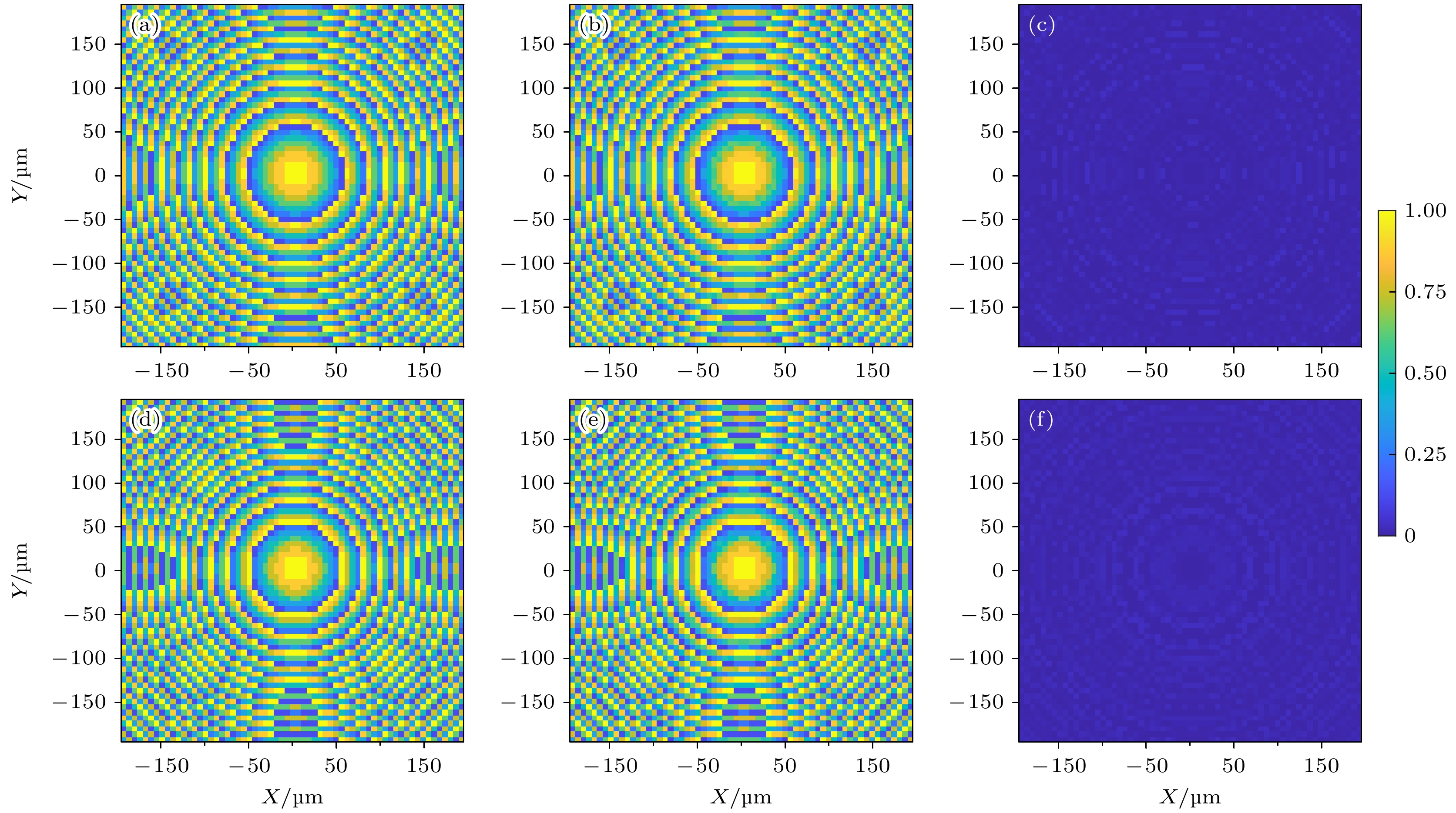
图 3 超透镜-目标相位偏移量分布图 (a) 波长10.6 μm, x线偏振态; (d) 波长9.3 μm, y线偏振态. 超透镜-实际相位偏移量分布图; (b) 波长10.6 μm, x线偏振态; (e) 波长9.3 μm, y线偏振态. 超透镜目标相位偏移量-实际相位偏移量差值图; (c) 波长10.6 μm, x线偏振态; (f) 波长9.3 μm, y线偏振态
Figure 3. Target phase shift of metalens: (a) Wavelength 10.6 μm with x linear polarizations; (d) wavelength 9.3 μm with y linear polarizations. Real phase shift of metalens; (b) wavelength 10.6 μm with x linear polarizations; (e) wavelength 9.3 μm with y linear polarizations. Difference value of Target phase shift and Real phase shift of metalens; (c) wavelength 10.6 μm with x linear polarizations; (f) wavelength 9.3 μm with y linear polarizations.
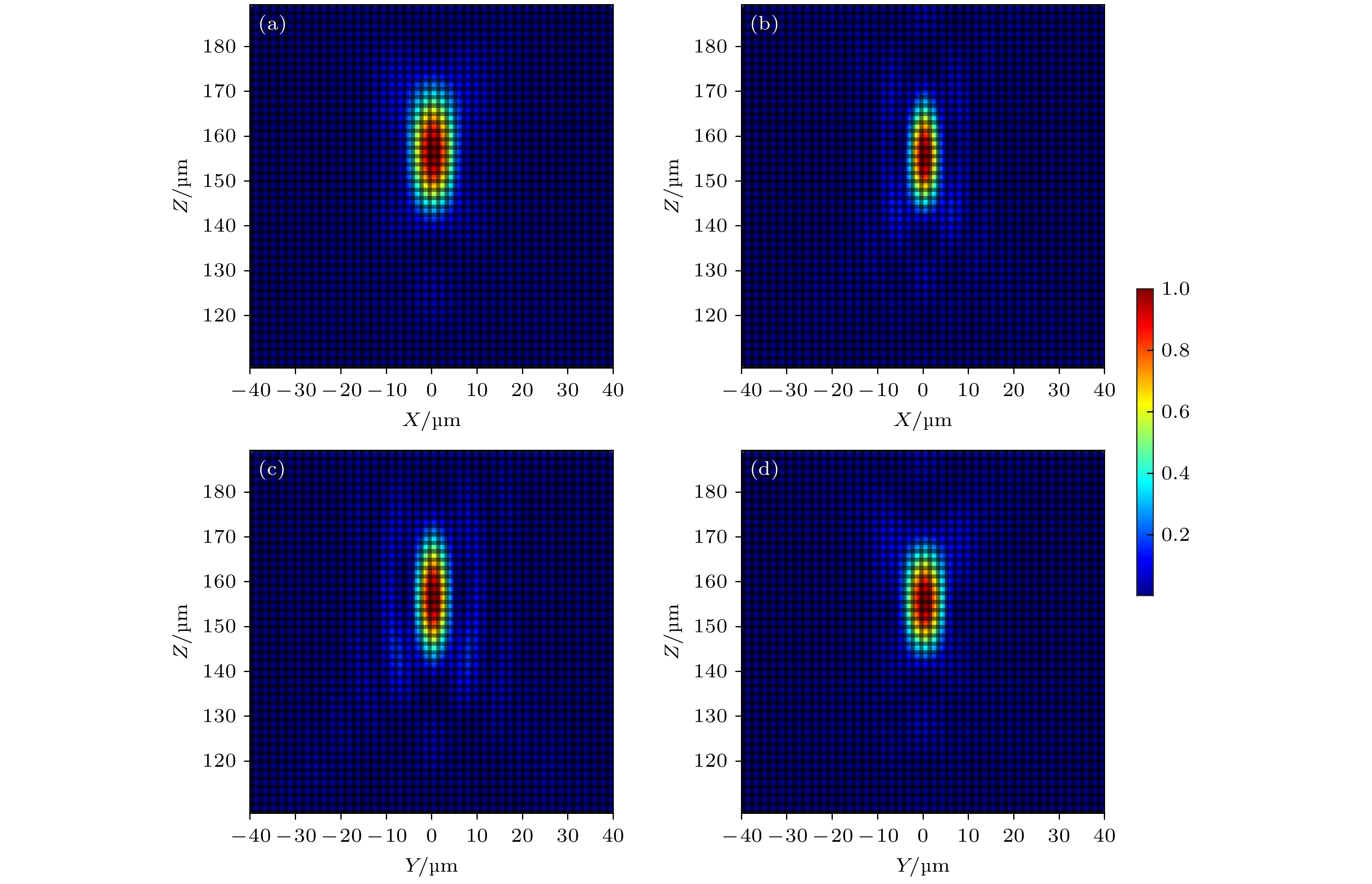
图 4 仿真得到的超透镜像平面聚焦光斑图 (a) 波长10.6 μm, x线偏振态, x-z接收面; (b) 波长10.6 μm, x线偏振态、y-z接收面; (c) 波长9.3 μm, y线偏振态, x-z接收面; (d) 波长9.3 μm, y线偏振态、y-z接收面
Figure 4. Focus spot pattern of image plane of metalens obtained by simulation: (a) Wavelength 10.6 μm with x linear polarizations at x-z plane; (b) wavelength 10.6 μm with x linear polarizations at y-z plane; (c) wavelength 9.3 μm with y linear polarizations at x-z plane; (d) wavelength 9.3 μm with y linear polarizations at y-z plane;
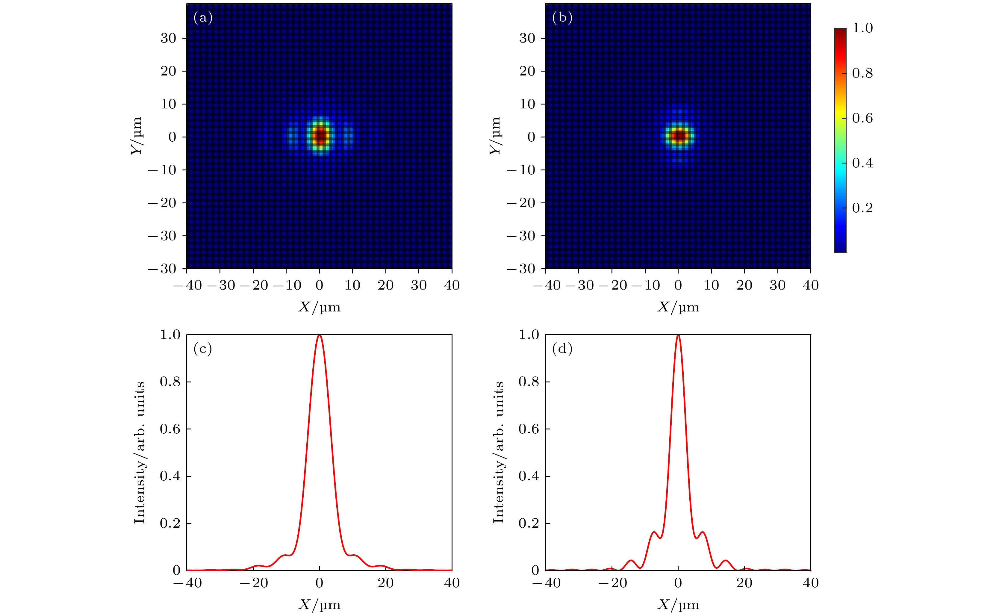
图 5 仿真得到的超透镜焦平面聚焦光斑图 (a)波长10.6 μm, x线偏振态、x-y接收面; (b) 波长9.3 μm, y线偏振态、x-y接收面. 聚焦光斑剖面图 (c) 波长10.6 μm, x线偏振态、x-y接收面; (d) 波长9.3 μm, y线偏振态、x-y接收面
Figure 5. Focus spot pattern of focal plane of metalens obtained by simulation: (a) Wavelength 10.6 μm with x linear polarizations at x-y plane; (b) wavelength 9.3 μm with y linear polarizations at x-y plane. Section views of focus spot; (c) wavelength 10.6 μm with x linear polarizations at x-y plane; (d) wavelength 9.3 μm with y linear polarizations at x-y plane.
图 6 定量分析超透镜的微元结构参数变化对聚焦效率&半峰全宽的影响示意图 (a) 超透镜椭圆纳米硅柱的高度H变化影响示意图; (b) 超透镜椭圆纳米硅柱的参数Dx变化影响示意图; (c)超透镜椭圆纳米硅柱的参数Dy变化影响示意图
Figure 6. Schematic diagram of quantitative analysis of the influence of the variation of the parameters of unit cell of the metalens on the focusing efficiency & the full width at half maximum: (a) Schematic diagram of the influence of the height H variation on elliptic silicon nanopillar of the metalens; (b) schematic diagram of the influence of the parameter Dx variation on elliptic silicon nanopillar of the metalens; (c) schematic diagram of the influence of the parameter Dy variation on elliptic silicon nanopillar of the metalens.
-
[1] Vitruk P 2017 Dental Town 17 62
[2] Linden E, Vitruk P 2015 Implant Pract. 8 30
[3] Bhadra R, Biswas P, Sankar M R 2015 Lasers based manufacturing (New Delhi: Springer) pp381–398
[4] Khorasaninejad M, Capasso F 2017 Science 358 1146
 Google Scholar
[5] Lalanne P, Chavel P 2017 Laser Photonics Rev. 11 1600295
 Google Scholar
[6] Ming L T, Hsiao H H, Cheng H C, Mu K C, Sun G, & Liu A Q, Tsai D P 2018 Adv. Opt. Mater. 6 1800554
 Google Scholar
[7] Chen M K, Wu Y, Feng L, Fan Q, Lu M, Xu T, Tsai D P 2021 Adv. Opt. Mater. 9 2001414
 Google Scholar
[8] Banerji S, Meem M, Sensale-Rodriguez B, Majμmder A, Vasquez F G, Menon R 2019 Optica 6 805
 Google Scholar
[9] Zou X, Zheng G, Yuan Q, Zang W, Zhu S 2020 Photoni X 1 2
 Google Scholar
[10] Chen W T, Zhu A Y, Capasso F 2020 Nat. Rev. Mater. 5 604
 Google Scholar
[11] Aieta F, Kats M A, Genevet P, Capasso F 2015 Science 347 1342
 Google Scholar
[12] Khorasaninejad M, Aieta F, Kanhaiya P, Kats M A, Genevet P, Rousso D, Capasso F 2015 Nano Lett. 15 5358
 Google Scholar
[13] Genevet P, Capasso F, Aieta F, Khorasaninejad M, Devlin R 2017 Optica 4 139
 Google Scholar
[14] Arbabi E, Arbabi A, Kamali S M, Horie Y, Faraon A 2016 Optica 3 628
 Google Scholar
[15] Lin D, Holsteen A L, Maguid E, Wetzstein G, Kik P G, Hasman E, Brongersma M L 2016 Nano Lett. 16 7671
 Google Scholar
[16] Arbabi E, Arbabi A, Kamali S M, Horie Y, Faraon A 2016 Sci. Rep. 6 32803
 Google Scholar
[17] Avayu O, Almeida E, Prior Y, Ellenbogen T 2017 Nat. Commun. 8 14992
 Google Scholar
[18] Yang H, Li G, Cao G, Yu F, Zhao Z, Ou K, Chen X, Lu Wei 2018 Opt. Mater. Express 8 1940
 Google Scholar
[19] Fan Q, Liu M, Yang C, Yu L, Yan F, Xu T 2018 Appl. Phys. Lett. 113 01104
[20] Fan Q, Wang Y, Liu M, Xu T 2018 Opt. Lett. 43 6005
 Google Scholar
[21] Zuo H, Choi D Y, Gai X, Ma P, Xu L, Neshev D N, Zhang B, Luther-Davies B 2017 Adv. Opt. Mater. 5 1700585
 Google Scholar
[22] Yu N F, Genevet P, Kats M A, Aieta F 2011 Science 334 333
 Google Scholar
[23] Aieta F, Genevet P, Yu N, Kats M A, Gaburro Z, Capasso F 2012 Nano Lett. 12 1702
 Google Scholar
[24] Luo X 2015 Sci. Chin.-Phys., Mech. Astron. 58 594201
 Google Scholar
[25] Khorasaninejad M, Capasso F 2015 Nano Lett. 15 6709
 Google Scholar
[26] Khorasaninejad M, Zhu A Y, Roques-Carmes C, et al. 2016 Nano Lett. 16 7229
 Google Scholar
[27] Mueller J, Rubin N A, Devlin R C, Groever B, Capasso F 2017 Phys. Rev. Lett 118 113901
 Google Scholar
[28] Yan C, Li X, Pu M, Ma X, Zhang F, Gao P, Liu K, Luo X 2019 Appl. Phys. Lett. 114 161904
 Google Scholar
[29] Zhao W, Jiang H, Liu B, Song J, Jiang Y, Tang C, Li J 2016 Sci. Rep. 6 30613
 Google Scholar
[30] 徐平, 肖钰斐, 黄海漩, 杨拓, 张旭琳, 袁霞, 李雄超, 王梦禹, 徐海东 2021 物理学报 70 084201
 Google Scholar
Xu P, Xiao Y F, Huang H X, Yang T, Zhang X L, Yuan X, Li X C, Wang M Y, Xu H D 2021 Acta Phys. Sin. 70 084201
 Google Scholar
[31] Sajedian I, Lee H, Rho J 2019 Sci. Rep. 9 10899
 Google Scholar
[32] 刘逸天, 陈琦凯, 唐志远, 赵庆, 片思杰, 刘鑫航, 林宏焘, 郝翔, 刘旭, 马耀光 2021 中国光学 14 831
 Google Scholar
Liu Y T, Chen Q K, Tang Z Y, Zhao Q, Pian S J, Liu X H, Lin H T, Hao X, Liu X, Ma Y G 2021 Chin. Opt. 14 831
 Google Scholar
Catalog
Metrics
- Abstract views: 8555
- PDF Downloads: 222
- Cited By: 0


 DownLoad:


