-
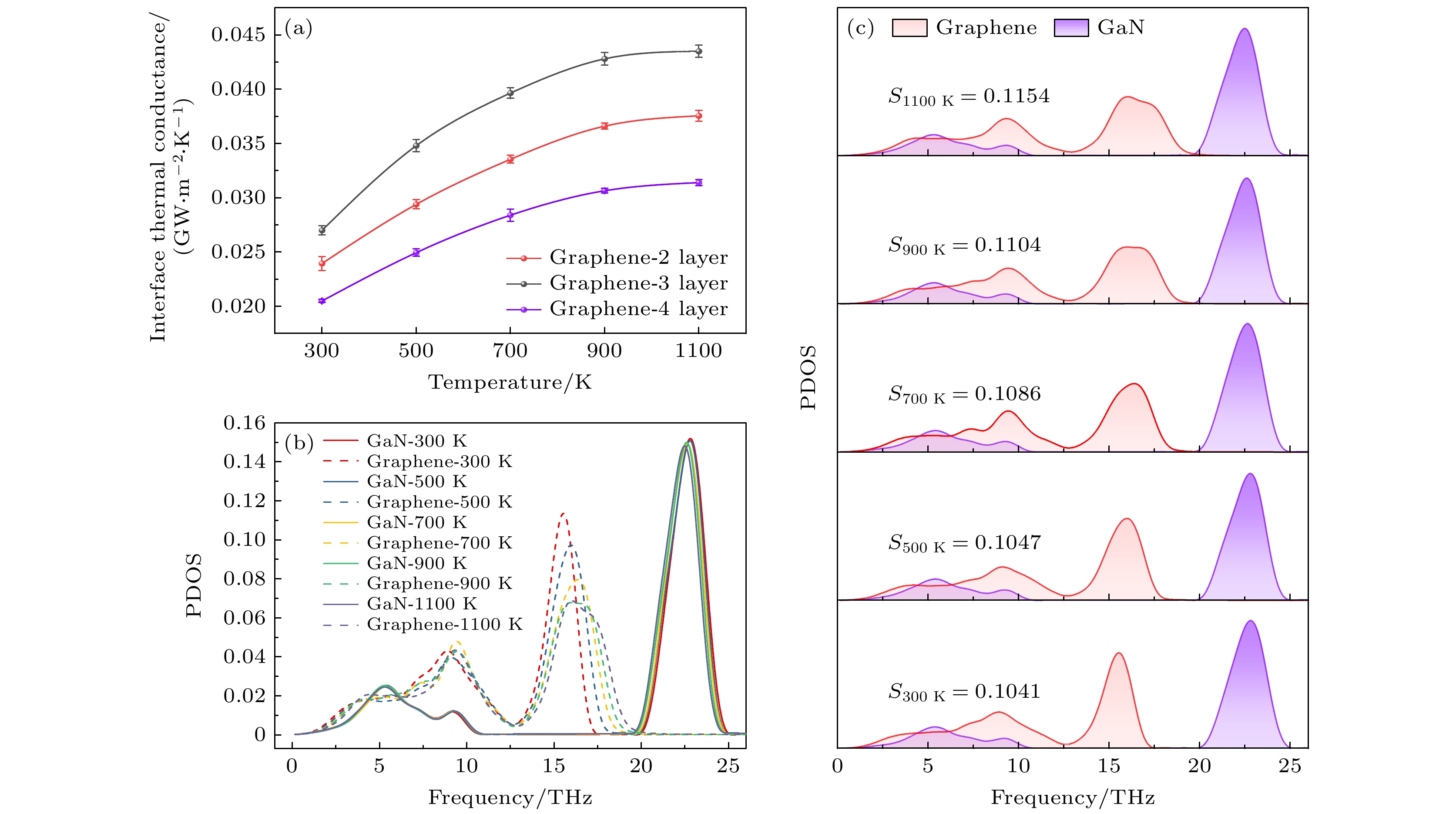
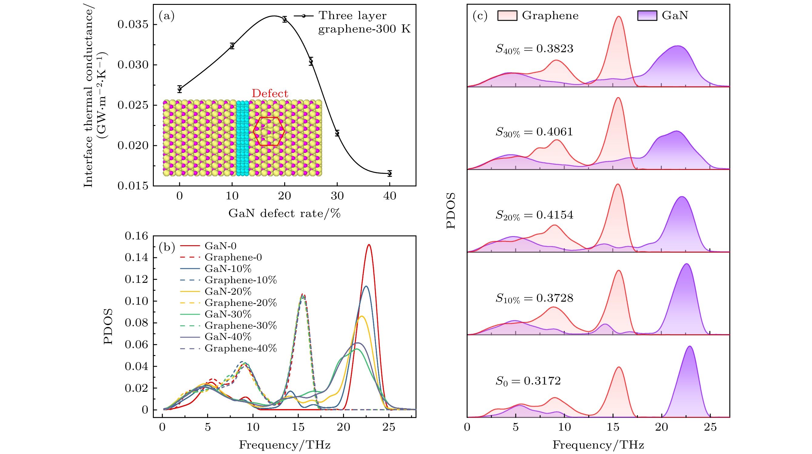
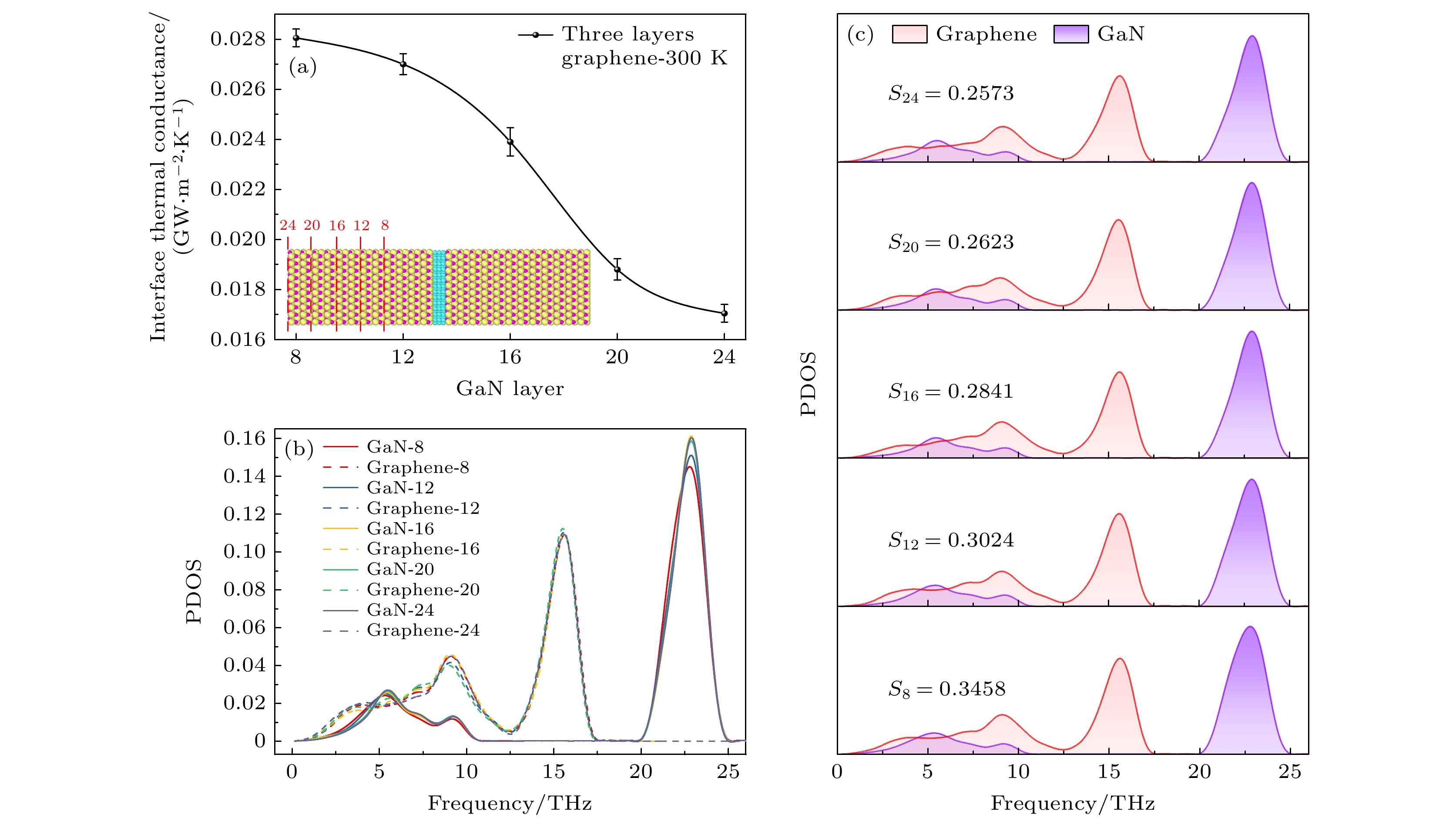
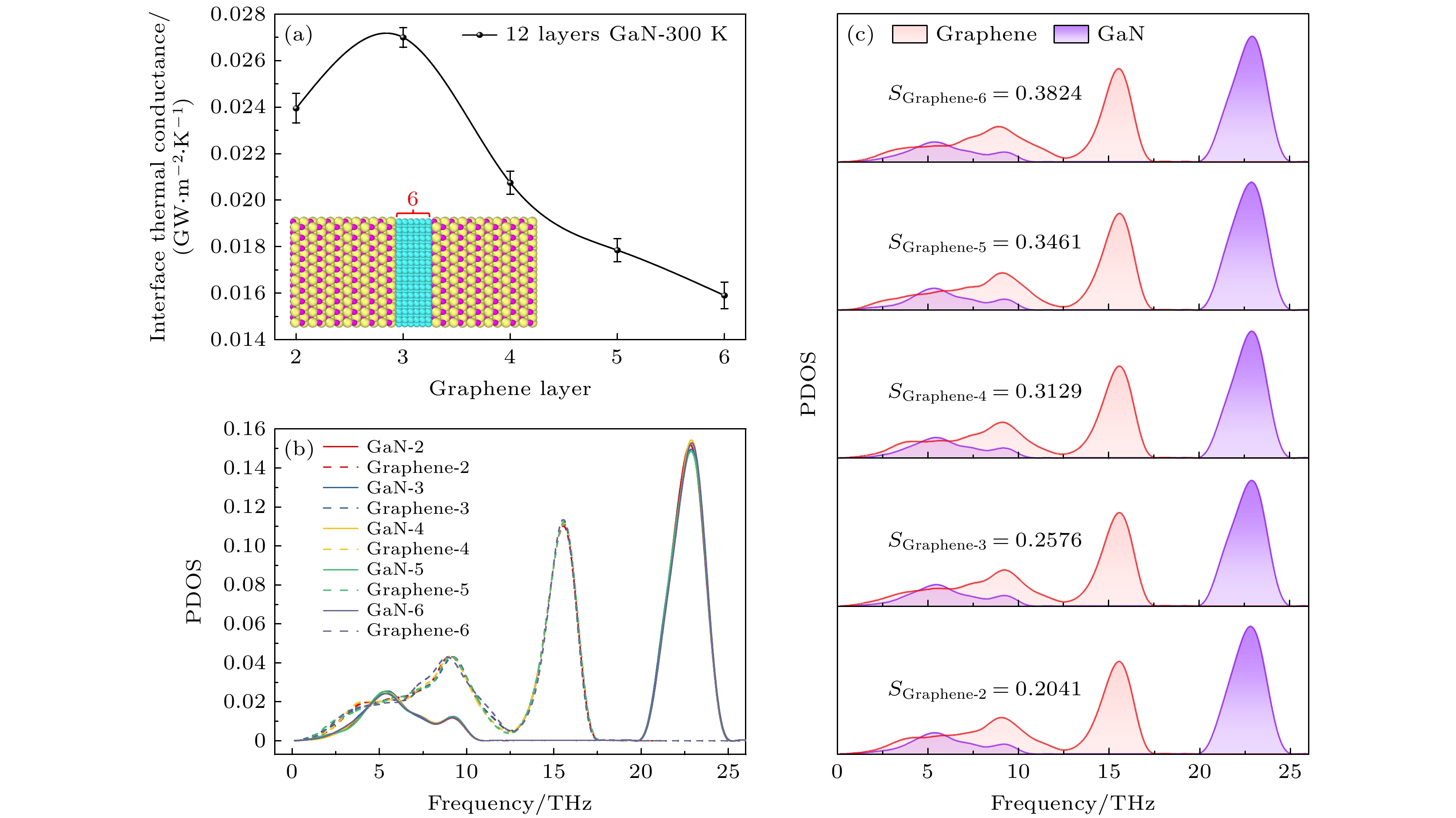
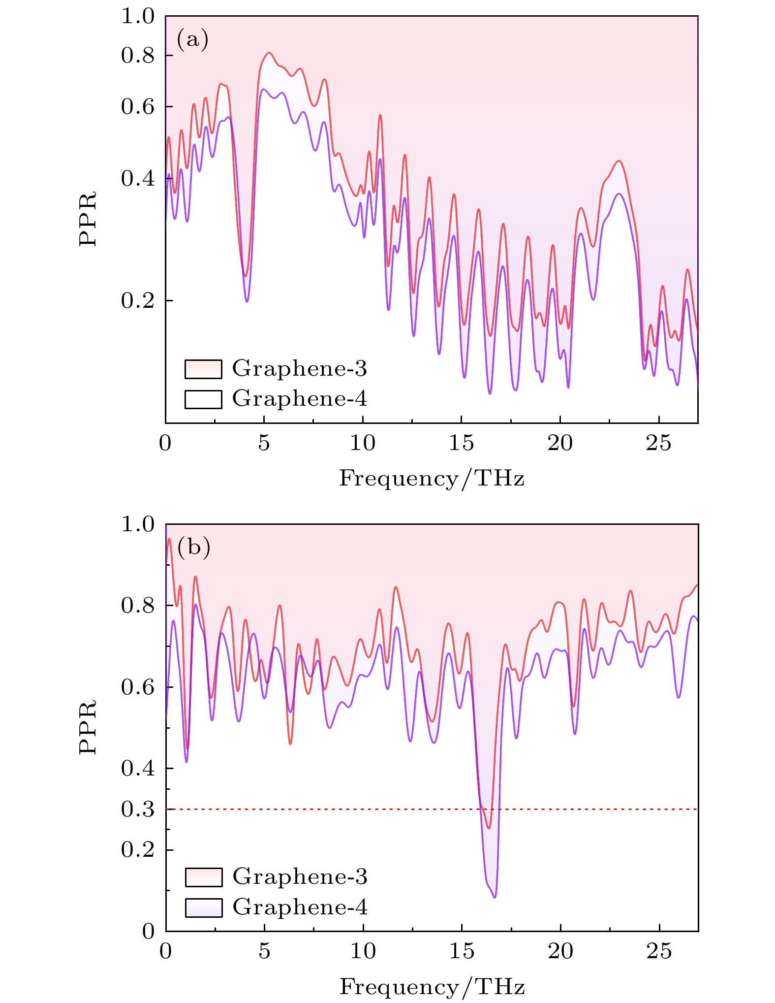
The performance of interfacial thermal transport in heterostructure determines the reliability of micro- and nano-scale device. In this study, a molecular dynamics method is used to investigate the interfacial thermal transport properties of graphene/GaN sandwich heterostructure. The effects of temperature, defect, and size on the interface thermal conductance at the heterostructure are analyzed. It is found that the interface thermal conductance increases with temperature rising; at 1100 K, the interface thermal conductance of the 3-layer graphene heterostructure is increased by 61%. This increase is mainly attributed to the enhanced lattice vibrations at higher temperature, which excites more out-of-plane phonons. The presence of minor vacancy defects in GaN leads interface thermal conductance to increase, reaching a maximum value of 0.0357 GW/(m2·K) at a defect rate of 20%. This enhancement is believed to be due to additional thermal transport pathways created by the defects. However, as the defect rate increases further, the interface thermal conductance begins to decrease, which is thought to be due to interfacial coupling strength decreasing. With the number of GaN layers increasing from 8 to 24, the interface thermal conductance decreases, the change is attributed to the decrease of the number of phonons participating in the thermal transport across the interface. Conversely, with the number of graphene layers increasing from 2 to 6, the interface thermal conductance initially increases and then decreases. This behavior is related to initial improvements of phonon matching and coupling strength, followed by the increase in phonon scattering and localization. The results of this study provide a theoretical basis for regulating the interfacial thermal transport in microelectronic devices.
-
Keywords:
- heterostructure /
- interface thermal conductance /
- vacancy defect /
- size effect
[1] Nguyen M H, Kwak S 2020 Electronics 9 2068
 Google Scholar
[2] Kimoto T, Watanabe H 2020 Appl. Phys. Exp. 13 120101
 Google Scholar
[3] Porwal H, Grasso S, Reece M J 2013 Adv. Appl. Ceram 112 443
 Google Scholar
[4] Inagaki M, Kang F 2014 J. Mater. Chem. A 2 13193
 Google Scholar
[5] Liu J, Tang J, Gooding J J 2012 J. Mater. Chem. 22 12435
 Google Scholar
[6] Hernaez M 2020 Sensors (Basel) 20 3196
 Google Scholar
[7] Santis J A, Marín-García C A, Sánchez-R V M 2023 J. Cryst. Growth 601 126944
 Google Scholar
[8] Alexander A B, Suchismita G, Wenzhong B, Irene C, Desalegne T, Feng M, Chun N L 2008 Nano Lett. 8 902
 Google Scholar
[9] Bao W L, Wang Z L, Chen G F 2021 Int. J. Heat Mass Tran. 173 121266
 Google Scholar
[10] Guo Z X, Ding J W, Gong X G 2012 Phys. Rev. B 85 235429
 Google Scholar
[11] Luo T, Lloyd J R 2012 Adv. Funct. Mater. 22 2495
 Google Scholar
[12] Wang T Y, Tsai J L 2016 Comput. Mater. Sci. 122 272
 Google Scholar
[13] Wang L, Li B W 2007 Phys Rev. Lett. 99 177208
 Google Scholar
[14] Liu D J 2020 Phys. Lett. A 384 126077
 Google Scholar
[15] Yue Y N, Zhang J C, Wang X W 2011 Small 7 3324
 Google Scholar
[16] Wang Z, Guan H W 2014 Appl. Mech. Mater. 487 63
 Google Scholar
[17] Wang Y, Yang C H, Cheng Y, Zhang Y Y 2015 RSC. Adv. 5 82638
 Google Scholar
[18] Liu D J, Wang S M, Zhu J J, Li H, Zhu H D 2022 Phys. Lett. A 426 127895
 Google Scholar
[19] Huang X Y, Zhi C Y, Lin Y, Bao H, Wu G N, Jiang P K, Mai Y W 2020 Mat. Sci. Eng. R 142 100577
 Google Scholar
[20] Tao L, Theruvakkattil S S, Shahsavari R 2017 ACS. Appl. Mater. Interfaces 9 989
 Google Scholar
[21] Yang B, Yang H Y, Li T B, Yang J M, Yang P 2021 Appl. Surf. Sci. 536 147828
 Google Scholar
[22] Bao W L, Wang Z L, Hu B Y, Tang D W 2023 Int. J. Heat Mass Tran. 201 123569
 Google Scholar
[23] Steve P 1995 J. Comput.Phys 117 1
 Google Scholar
[24] Lin C P, Rao Z H 2017 Appl. Therm. Eng. 110 1411
 Google Scholar
[25] Stuart S J, Tutein A B, Harrison J A 2000 J. Chem. Phys. 112 6472
 Google Scholar
[26] Donald W B, Olga A S, Judith A H, Steven J S, Boris N, Susan B S 2002 J. Phys-Condens. Mat. 14 783
 Google Scholar
[27] Stillinger F H, Weber T A 1985 Phys. Rev. B 31 5262
 Google Scholar
[28] Yang Y Z, Ma J, Yang J, Zhang Y Y 2022 ACS Appl. Mater. Interfaces 14 45742
 Google Scholar
[29] Han D, Wang X Y, Ding W Y, Chen Y, Zhang J C, Xin G M, Cheng L 2019 Nanotechnology 30 075403
 Google Scholar
[30] Xin W Y, Jing Z C, Yue C, Paddy K L C 2017 Nanoscale 9 2262
 Google Scholar
[31] Guo Y, Bescond M, Zhang Z, Xiong S, Hirakawa K, Nomura M, Volz S 2021 APL Mater. 9 091104
 Google Scholar
-
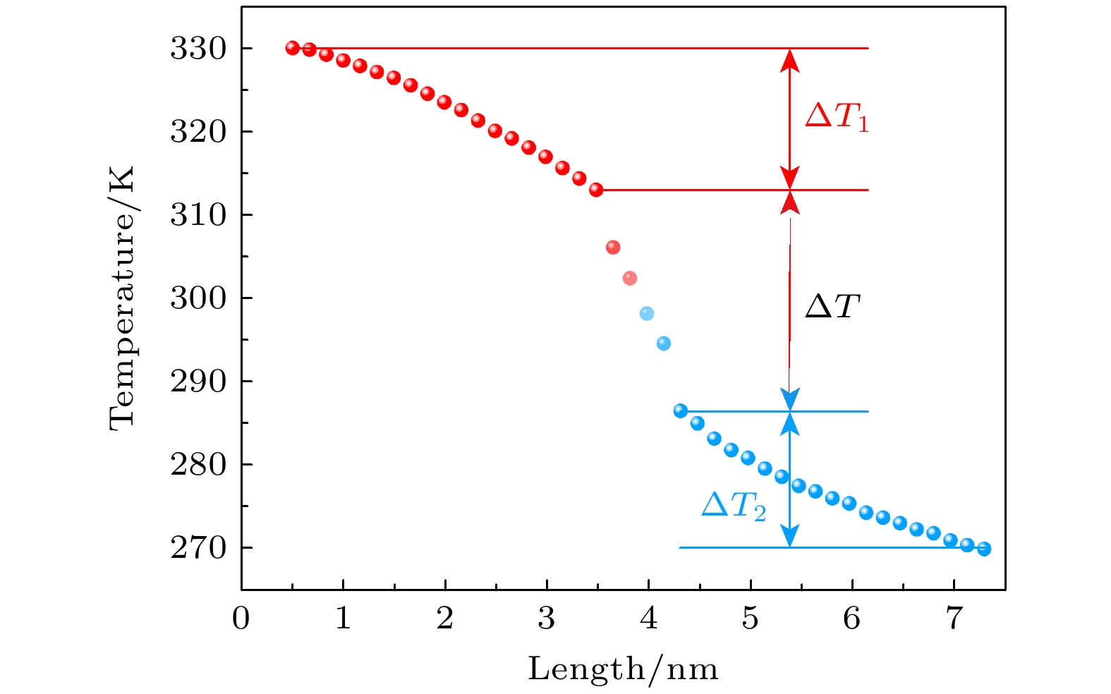
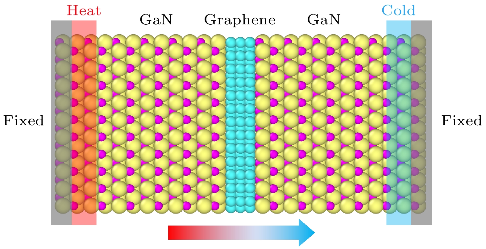
图 2 石墨烯/GaN异质结构沿热流方向的温度分布(∆T1为GaN层热源温度变化, ∆T2为GaN层冷源温度变化, ∆T为石墨烯中间层温度变化)
Figure 2. Temperature distribution of graphene/GaN heterostructure along the heat flow direction (∆T1 is the temperature change of the heat source of GaN layer, ∆T2 is the cold source temperature change of GaN layer, and ∆T is the temperature change of the middle layer of graphene).
图 3 (a) ITC与异质结构温度变化的关系; (b)石墨烯和GaN在不同温度下的PDOS; (c)石墨烯和GaN在不同温度下的PDOS重叠区域和重叠因子S
Figure 3. (a) Relationship between the ITC and temperature change of heterostructure; (b) PDOS of graphene and GaN at different temperatures; (c) PDOS overlap regions and the overlap factor S for graphene and GaN at different temperatures.
图 4 (a)异质结构的ITC与GaN空位缺陷率的关系; (b)不同GaN空位缺陷率下石墨烯和GaN的PDOS; (c)在不同的GaN空位缺陷率下, 石墨烯和GaN的PDOS重叠区域和重叠因子S
Figure 4. (a) Relationship between the ITC and GaN vacancy defect rate of heterostructure; (b) PDOS of graphene and GaN at different GaN vacancy defect rate; (c) PDOS overlap regions and the overlap factor S for graphene and GaN at different GaN vacancy defect rate.
图 5 (a) ITC与异质结构GaN层数的关系; (b)不同数量GaN层中, 石墨烯和GaN的PDOS; (c)在不同数量的GaN层中, 石墨烯和GaN的PDOS重叠区域和重叠因子S
Figure 5. (a) Relationship between the ITC and the number of GaN layer of heterostructure; (b) PDOS of graphene and GaN at different number of GaN layer; (c) PDOS overlap regions and the overlap factor S for graphene and GaN at different number of GaN layer.
图 6 (a) ITC与异质结构石墨烯层数的关系; (b)不同数量石墨烯层下石墨烯和GaN的PDOS; (c)不同数量石墨烯层下石墨烯和GaN的PDOS重叠区域和重叠因子S
Figure 6. (a) Relationship between the ITC and the number of graphene layer of heterostructure; (b) PDOS of graphene and GaN at different number of graphene layer; (c) PDOS overlap regions and the overlap factor S for graphene and GaN at different number of graphene layer.
-
[1] Nguyen M H, Kwak S 2020 Electronics 9 2068
 Google Scholar
[2] Kimoto T, Watanabe H 2020 Appl. Phys. Exp. 13 120101
 Google Scholar
[3] Porwal H, Grasso S, Reece M J 2013 Adv. Appl. Ceram 112 443
 Google Scholar
[4] Inagaki M, Kang F 2014 J. Mater. Chem. A 2 13193
 Google Scholar
[5] Liu J, Tang J, Gooding J J 2012 J. Mater. Chem. 22 12435
 Google Scholar
[6] Hernaez M 2020 Sensors (Basel) 20 3196
 Google Scholar
[7] Santis J A, Marín-García C A, Sánchez-R V M 2023 J. Cryst. Growth 601 126944
 Google Scholar
[8] Alexander A B, Suchismita G, Wenzhong B, Irene C, Desalegne T, Feng M, Chun N L 2008 Nano Lett. 8 902
 Google Scholar
[9] Bao W L, Wang Z L, Chen G F 2021 Int. J. Heat Mass Tran. 173 121266
 Google Scholar
[10] Guo Z X, Ding J W, Gong X G 2012 Phys. Rev. B 85 235429
 Google Scholar
[11] Luo T, Lloyd J R 2012 Adv. Funct. Mater. 22 2495
 Google Scholar
[12] Wang T Y, Tsai J L 2016 Comput. Mater. Sci. 122 272
 Google Scholar
[13] Wang L, Li B W 2007 Phys Rev. Lett. 99 177208
 Google Scholar
[14] Liu D J 2020 Phys. Lett. A 384 126077
 Google Scholar
[15] Yue Y N, Zhang J C, Wang X W 2011 Small 7 3324
 Google Scholar
[16] Wang Z, Guan H W 2014 Appl. Mech. Mater. 487 63
 Google Scholar
[17] Wang Y, Yang C H, Cheng Y, Zhang Y Y 2015 RSC. Adv. 5 82638
 Google Scholar
[18] Liu D J, Wang S M, Zhu J J, Li H, Zhu H D 2022 Phys. Lett. A 426 127895
 Google Scholar
[19] Huang X Y, Zhi C Y, Lin Y, Bao H, Wu G N, Jiang P K, Mai Y W 2020 Mat. Sci. Eng. R 142 100577
 Google Scholar
[20] Tao L, Theruvakkattil S S, Shahsavari R 2017 ACS. Appl. Mater. Interfaces 9 989
 Google Scholar
[21] Yang B, Yang H Y, Li T B, Yang J M, Yang P 2021 Appl. Surf. Sci. 536 147828
 Google Scholar
[22] Bao W L, Wang Z L, Hu B Y, Tang D W 2023 Int. J. Heat Mass Tran. 201 123569
 Google Scholar
[23] Steve P 1995 J. Comput.Phys 117 1
 Google Scholar
[24] Lin C P, Rao Z H 2017 Appl. Therm. Eng. 110 1411
 Google Scholar
[25] Stuart S J, Tutein A B, Harrison J A 2000 J. Chem. Phys. 112 6472
 Google Scholar
[26] Donald W B, Olga A S, Judith A H, Steven J S, Boris N, Susan B S 2002 J. Phys-Condens. Mat. 14 783
 Google Scholar
[27] Stillinger F H, Weber T A 1985 Phys. Rev. B 31 5262
 Google Scholar
[28] Yang Y Z, Ma J, Yang J, Zhang Y Y 2022 ACS Appl. Mater. Interfaces 14 45742
 Google Scholar
[29] Han D, Wang X Y, Ding W Y, Chen Y, Zhang J C, Xin G M, Cheng L 2019 Nanotechnology 30 075403
 Google Scholar
[30] Xin W Y, Jing Z C, Yue C, Paddy K L C 2017 Nanoscale 9 2262
 Google Scholar
[31] Guo Y, Bescond M, Zhang Z, Xiong S, Hirakawa K, Nomura M, Volz S 2021 APL Mater. 9 091104
 Google Scholar
Catalog
Metrics
- Abstract views: 5612
- PDF Downloads: 329
- Cited By: 0


 DownLoad:
