


-
In recent years, MoSe2, as a kind of transition metal dichalcogenide, has aroused widespread research interest due to its special crystal structure with different electrical and optical properties. The band gap of molybdenum diselenide can be manipulated by different layers, strain engineering, doping, or the formation of heterostructures, which makes it potential advantages in optoelectronic devices and photovoltaic applications. In this work, we investigate the influence of selenization temperature on the structures and optical properties of the MoSe2 films. Molybdenum (Mo) thin films are prepared by RF magnetron sputtering, and then MoSe2 thin films are generated by selenization annealing. The surface morphology, crystal structure, and optical bandgap for each of the MoSe2 thin films are characterized and analyzed by using scanning electron microscopy, X-ray diffraction, and ultraviolet visible spectroscopy, respectively. The results show that the crystal structures of the MoSe2 thin films are closely related to the selenization temperature (Ts): with the increase of selenization temperature, the average grain size in the thin film decreases slightly and then increases rapidly from 24.82 nm to 55.76 nm. Meanwhile, the (002) crystal plane of MoSe2 also exhibits preferential growth with temperature increasing. Each MoSe2 thin film has a low absorption rate for short-wavelength light (around 600 nm). With the increase of selenization temperature, the bandgap waves of the MoSe2 thin films are blue-shifted, and the optical bandgaps decrease, which is attributed to the fact that different selenization temperatures cause the lattice size of MoSe2 to change, thereby affecting the spatial expansion of its electronic wave function. In addition, the structure and optical bandgap of MoSe2 can be effectively controlled by changing the selenization temperature, which provides more possibilities for the applications of the MoSe2 thin films in optical devices.
-
Keywords:
- MoSe2 thin film /
- selenization temperature /
- magnetron sputtering /
- thin film structure /
- optical bandgap
[1] Monga D, Sharma S, Shetti N P, Basu S, Reddy K R, Aminabhavi T M 2001 Mater. Today Chem. 19 100399
 Google Scholar
[2] Zhou W, Gong H M, Jin X H, Chen Y, Li H M, Liu S 2022 Front. Physics 10 842789
Google Scholar
[3] Kaur R, Singh K, Tripathi S 2022 J. Alloy. Compd. 905 164103
Google Scholar
[4] Cui Z, Wang H X, Shen Y, Qin K, Yuan P, Li E L 2024 Mater. Today Phys. 40 101317
Google Scholar
[5] Li F, Xu B, Yang W, Qi Z Y, Ma C, Wang Y J, Zhang X H, Luo Z R, Liang D L, Li D 2020 Nano Res. 13 1053
Google Scholar
[6] Yan Q J, Cheng J X, Wang W K, Sun M J, Yin Y L, Peng Y H, Zhou W C, Tang D S 2022 J. Phys. Condes. Matter 34 475703
Google Scholar
[7] Zhao P, Cheng R, Zhao L, Yang H J, Jiang Z Y 2023 J. Appl. Phys. 134 134302
Google Scholar
[8] Kalkan S B, Najafidehaghani E, Gan Z, Apfelbeck F A C, Hübner U, George A, Turchanin A, Nickel B 2021 npj 2D Mater. Appl. 5 92
Google Scholar
[9] 邓霖湄, 司君山, 吴绪才, 张卫兵 2022 物理学报 71 147101
Google Scholar
Deng L M, Si J S, Wu X C, Zhang W B 2022 Acta Phys. Sin. 71 147101
Google Scholar
[10] 郝国强, 张瑞, 张文静, 陈娜, 叶晓军, 李红波 2022 物理学报 71 017104
Google Scholar
Hao G Q, Zhang R, Zhang W J, Chen N, Ye X J, Li H B 2022 Acta Phys. Sin. 71 017104
Google Scholar
[11] Zhang Q Y, Mei L, Cao X H, Tang Y X, Zeng Z Y 2020 J. Mater. Chem. A 8 15417
Google Scholar
[12] Li Y G, Kuang G Z, Jiao Z J, Yao L, Duan R H 2022 Mater. Res. Express 9 122001
Google Scholar
[13] Wei Y X, Hu C G, Li Y N, Hu X T, Yu K H, Sun L T, Hohage M, Sun L D 2020 Nanotechnology 31 315710
Google Scholar
[14] Chen L, Wang J F, Li X J, Zhao C R, Hu X, Wu Y, He Y M 2022 Inorg. Chem. Front. 9 2714
Google Scholar
[15] Vanathi V, Sathishkumar M, Kannan S, Balamurugan A 2024 Mater. Lett. 356 135595
Google Scholar
[16] Li J C, Yan W J, Lü Y H, Leng J, Zhang D, Coileáin C Ó, Cullen C P, Stimpel-Lindner T, Duesberg G S, Cho J 2020 RSC Adv. 10 1580
Google Scholar
[17] Zhan W Y, Zou J P, Xu M, Lei T, Wei H M 2023 Trans. Nonferrous Met. Soc. China 33 2483
Google Scholar
[18] Zhu X B, Jiang X, Yao X Y, Leng Y X, Xu X X, Peng A P, Wang L P, Xue Q J 2019 ACS Appl. Mater. Interfaces 11 45726
Google Scholar
[19] Yaqub T B, Vuchkov T, Sanguino P, Polcar T, Cavaleiro A 2020 Coatings 10 133
Google Scholar
[20] Yaqub T B, Kannur K H, Vuchkov T, Pupier C, Héau C, Cavaleiro A 2020 Mater. Lett. 275 128035
Google Scholar
[21] Li N, Liu Z T, Feng L P, Jia R T 2016 Surf. Eng. 32 299
Google Scholar
[22] Mao X, Li Z Q, Zou J P, Zhao G Y, Li D N, Song Z Q 2019 Appl. Surf. Sci. 487 719
Google Scholar
[23] Wu Q L, Fu X S, Yang K, Wu H Y, Liu L, Zhang L, Tian Y, Yin L J, Huang W Q, Zhang W, Wong P K J, Zhang L J, Wee A T S, Qin Z H 2021 ACS Nano 15 4481
Google Scholar
[24] Franklin A D 2015 Science 349 704
Google Scholar
[25] Chang Y S, Chen C Y, Ho C J, Cheng C M, Chen H R, Fu T Y, Huang Y T, Ke S W, Du H Y, Lee K Y 2021 Nano Energy 84 105922
Google Scholar
[26] Thureja D, Imamoglu A, Smoleński T, Amelio I, Popert A, Chervy T, Lu X, Liu S, Barmak K, Watanabe K 2022 Nature 606 298
Google Scholar
[27] Chouki T, Donkova B, Aktarla B, Stefanov P, Emin S 2021 Mater. Today Commun. 26 101976
Google Scholar
[28] Upadhyay S, Pandey O 2021 J. Alloy. Compd. 857 157522
Google Scholar
[29] Jäger-Waldau A, Lux-Steiner M, Jäger-Waldau R, Burkhardt R, Bucher E 1990 Thin Solid Films 189 339
Google Scholar
[30] 李健, 朱洁 2007 物理学报 56 574
Google Scholar
Li J, Zhu J 2007 Acta Phys. Sin. 56 574
Google Scholar
[31] 毛启楠, 张晓勇, 李学耕, 贺劲鑫, 于平荣, 王东 2014 物理学报 63 118802
Google Scholar
Mao Q N, Zhang X Y, Li X G, He J X, Yu P R, Wang D 2014 Acta Phys. Sin. 63 118802
Google Scholar
[32] Sharma C, Srivastava A K, Gupta M K 2023 Physica B 669 415290
Google Scholar
[33] Zeng F, Kong W Y, Liang Y H, Li F, Lvtao Y Z, Su Z H, Wang T, Peng B G, Ye L F, Chen Z H, Gao X Y, Huang J, Zheng R K, Yang X D 2023 Adv. Mater. 35 2306051
Google Scholar
[34] Mittal H, Raza M, Khanuja M 2023 MethodsX 11 102409
Google Scholar
[35] Kandar S, Bhatt K, Kumar N, Kapoor A K, Singh R 2024 ACS Appl. Nano Mater. 7 8212
Google Scholar
[36] Tao S M, Ma J F, Liu J J, Wang Y R, Xiao J R 2024 Int. J. Hydrog. Energy 58 829
Google Scholar
[37] Ohtake A, Sakuma Y 2021 J. Phys. Chem. C 125 11257
Google Scholar
[38] Shi N X, Liu G Z, Xi B J, An X G, Sun C H, Xiong S L 2024 Nano Res. 17 4023
Google Scholar
[39] Wang X, Gong Y, Shi G, Chow W L, Keyshar K, Ye G, Vajtai R, Lou J, Liu Z, Ringe E 2014 ACS Nano 8 5125
Google Scholar
[40] Zhao S D, Lu M L, Xue S S, Yan L, Miao P, Hang Y, Wang X J, Liu Z G, Wang Y, Tao L, Sui Y, Wang Y 2019 arXiv: 1904.09789 [cond-mat.mtrl-sci]
[41] Ahmad Y H, Kamand F Z, Zekri A, Chae K J, Aïssa B, Al-Qaradawi S Y 2023 Appl. Surf. Sci. 626 157205
Google Scholar
[42] Liu H L, Yang T, Chen J H, Chen H W, Guo H H, Saito R, Li M Y, Li L J 2020 Sci Rep 10 15282
Google Scholar
[43] Wang Z, Chen Y F, Wu P S, Ye J F, Peng M, Yan Y, Zhong F, He T, Wang Y, Xu M J 2020 Infrared Phys. Technol. 106 103272
Google Scholar
[44] 黄静雯, 罗利琼, 金波, 楚士晋, 彭汝芳 2017 物理学报 66 137801
Google Scholar
Huang J W, Luo L Q, Jin B, Chu S J, Peng R F 2017 Acta Phys. Sin. 66 137801
Google Scholar
[45] Zhang X L, Zhou J, Li S Q, Wang Y Y, Zhang S P, Liu Y L, Gao J F, Zhao J J, Wang W P, Yu R C 2021 J. Phys. Chem. Lett. 12 5879
Google Scholar
-
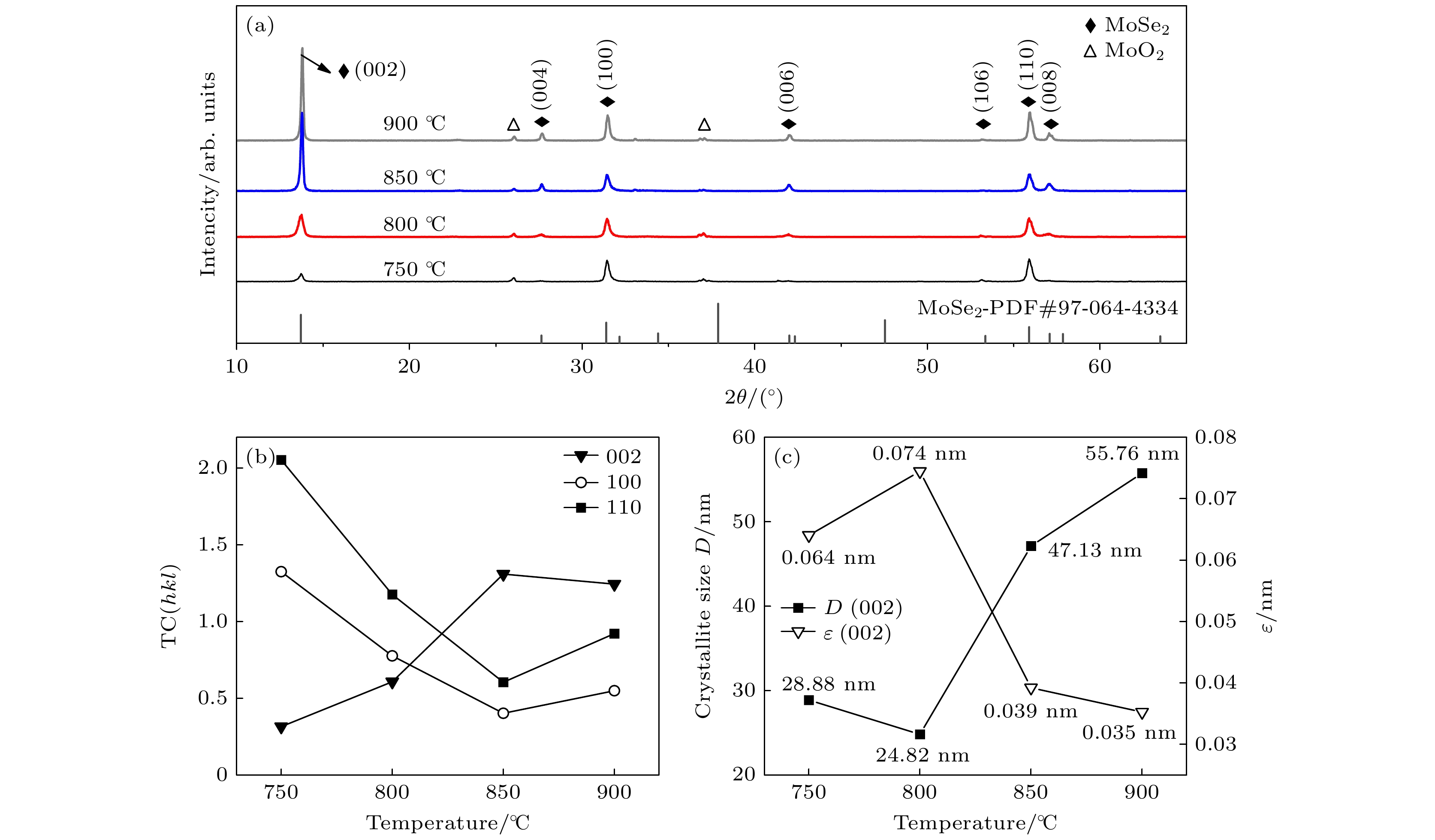
图 1 (a) MoSe2薄膜的XRD图谱; (b) MoSe2薄膜主要的衍射峰为(002), (100), (110)时不同硒化温度下的织构系数; (c) MoSe2薄膜平均晶粒尺寸随硒化温度的变化曲线和微应变值
Figure 1. (a) XRD pattern of MoSe2 thin film; (b) texture coefficient at different selenization temperatures when the main diffraction peaks of MoSe2 thin film are (002), (100), and (110); (c) variation curve and microstrain value of the average grain size of MoSe2 thin film with selenization temperature.
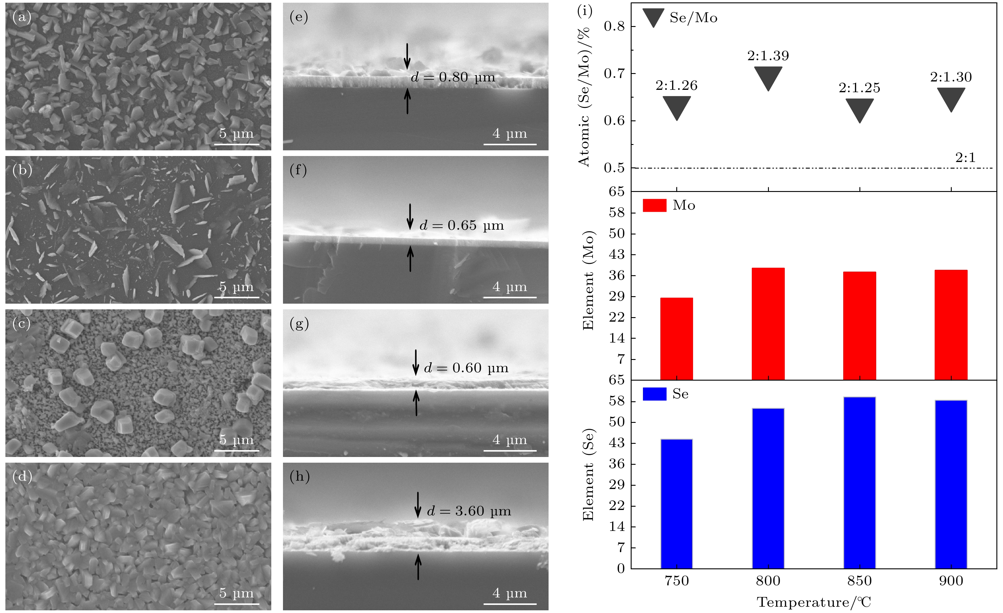
图 2 当硒化温度不同时, MoSe2薄膜的SEM图像(a)—(d)及典型横截面图像(e)—(h) (a), (e) 750 ℃; (b), (f) 800 ℃; (c), (g) 850 ℃; (d), (h) 900 ℃. (i)不同温度的MoSe2薄膜的Se, Mo元素原子占比图
Figure 2. SEM images (a)–(d) and typical cross-sectional images (e)–(h) of MoSe2 thin films at different selenization temperatures: (a), (e) 750 ℃; (b), (f) 800 ℃; (c), (g) 850 ℃; (d), (h) 900 ℃. (i) Atomic proportion of Se and Mo elements in MoSe2 thin films at different temperatures.

图 3 MoSe2薄膜的50 nm (a)和5 nm (b)分辨透射电子显微镜图片; MoSe2薄膜(002) (c)和(100) (d)面的选取电子衍射图样; (e)衍射环
Figure 3. 50 nm (a) and 5 nm (b) resolution TEM images of MoSe2 thin films; select electron diffraction patterns for the (002) (c) and (100) (d) planes of MoSe2 thin film; (e) diffraction ring.

图 4 MoSe2薄膜在900 ℃的XPS图谱 (a)总谱; (b) Se 3d; (c) Mo 3d
Figure 4. XPS spectrum of MoSe2 thin film at 900 ℃: (a) Overall spectrum; (b) Se 3d; (c) Mo 3d.
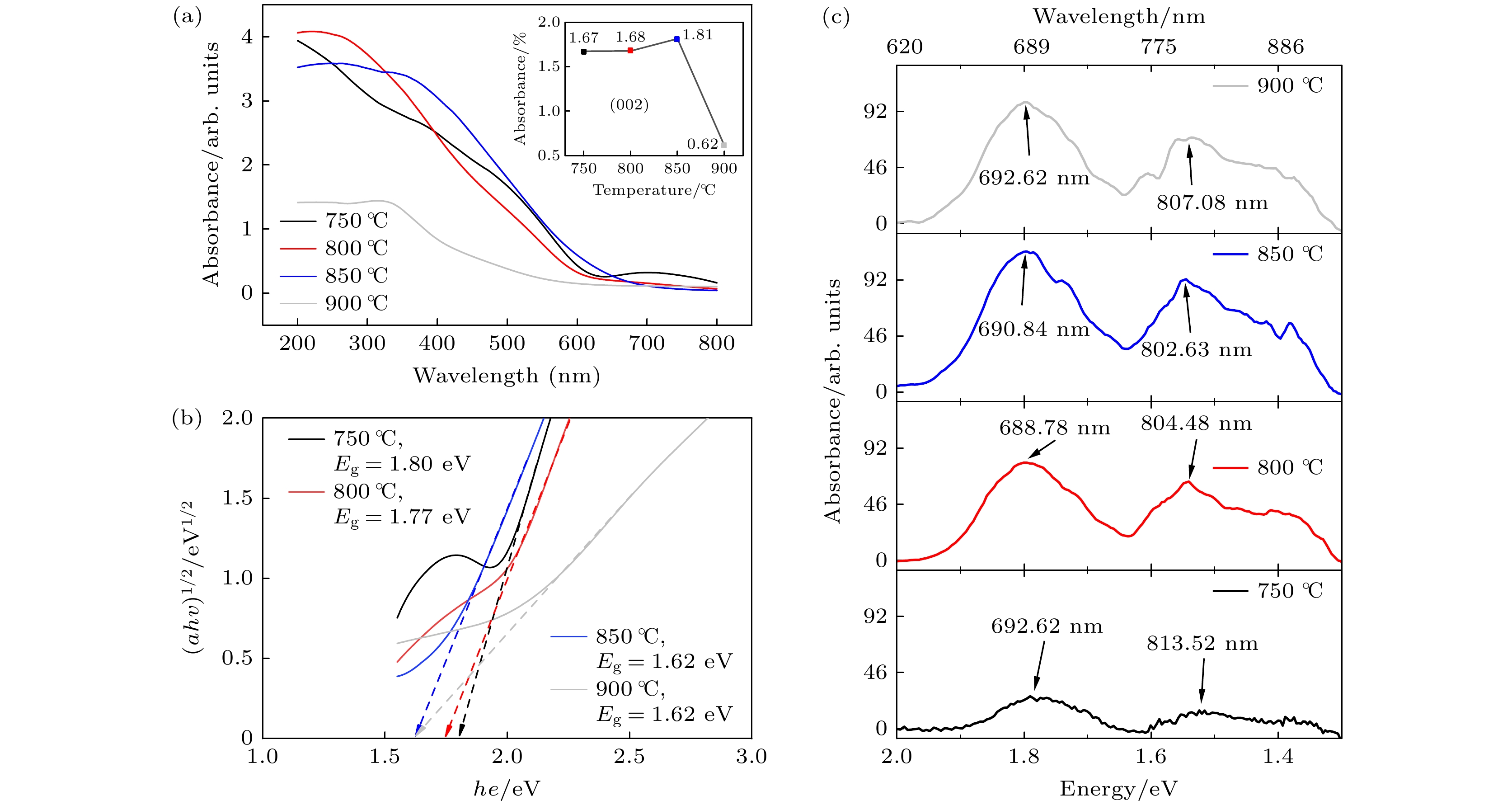
图 5 (a) MoSe2薄膜的吸收光谱, 插图不同温度下MoSe2薄膜的平均吸收率; (b) MoSe2薄膜的Tauc关系图; (c)不同硒化温度MoSe2薄膜的发致发光光谱
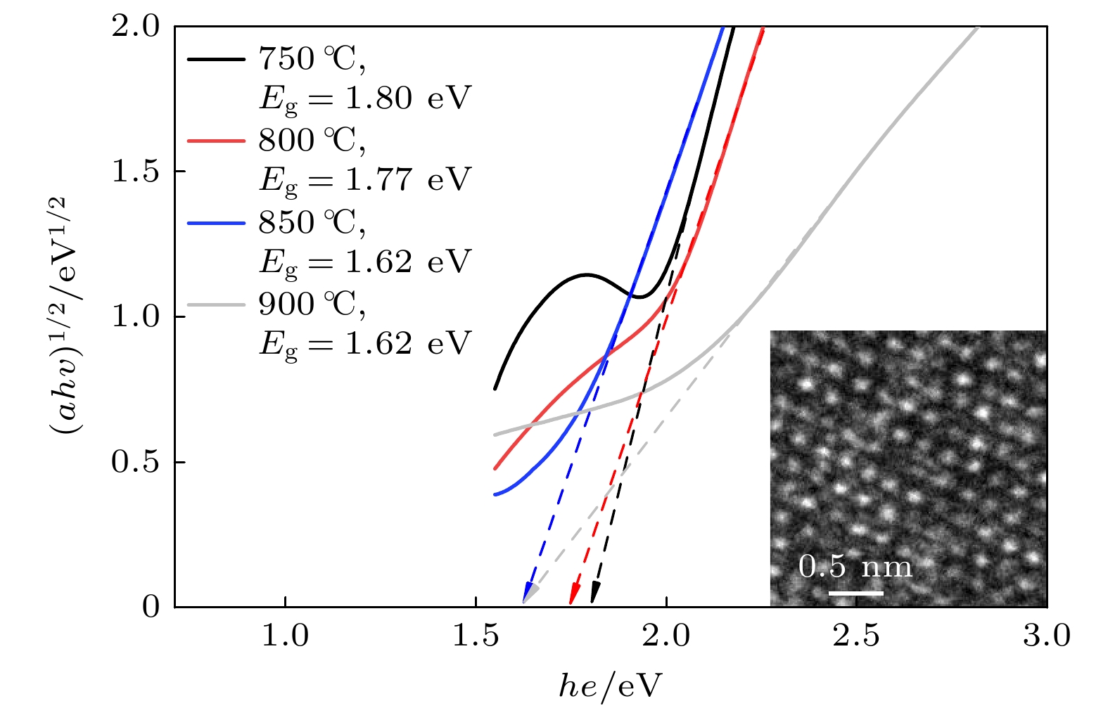
Figure 5. (a) Absorption spectrum of MoSe2 thin film, insert is the average absorption rate of MoSe2 thin film at different temperatures; (b) Tauc diagram of MoSe2 thin film; (c) photoluminescence spectra of MoSe2 thin films at different selenization temperatures.
表 1 750—900 ℃ MoSe2薄膜的各元素原子、质量占比
Table 1. Atomic and mass ratios of various elements in MoSe2 thin films at 750–900 ℃.
Temperature/℃ Element Atomic/% Weight/% 750 Se 44.46 52.70 Mo 28.30 40.76 O 27.24 6.54 800 Se 55.34 47.25 Mo 38.58 27.11 O 6.09 25.65 850 Se 59.16 54.97 Mo 37.23 26.47 O 3.61 16.56 900 Se 58.06 53.12 Mo 37.88 28.53 O 4.06 18.35  DownLoad: CSV
-
[1] Monga D, Sharma S, Shetti N P, Basu S, Reddy K R, Aminabhavi T M 2001 Mater. Today Chem. 19 100399
Google Scholar
[2] Zhou W, Gong H M, Jin X H, Chen Y, Li H M, Liu S 2022 Front. Physics 10 842789
Google Scholar
[3] Kaur R, Singh K, Tripathi S 2022 J. Alloy. Compd. 905 164103
Google Scholar
[4] Cui Z, Wang H X, Shen Y, Qin K, Yuan P, Li E L 2024 Mater. Today Phys. 40 101317
Google Scholar
[5] Li F, Xu B, Yang W, Qi Z Y, Ma C, Wang Y J, Zhang X H, Luo Z R, Liang D L, Li D 2020 Nano Res. 13 1053
Google Scholar
[6] Yan Q J, Cheng J X, Wang W K, Sun M J, Yin Y L, Peng Y H, Zhou W C, Tang D S 2022 J. Phys. Condes. Matter 34 475703
Google Scholar
[7] Zhao P, Cheng R, Zhao L, Yang H J, Jiang Z Y 2023 J. Appl. Phys. 134 134302
Google Scholar
[8] Kalkan S B, Najafidehaghani E, Gan Z, Apfelbeck F A C, Hübner U, George A, Turchanin A, Nickel B 2021 npj 2D Mater. Appl. 5 92
Google Scholar
[9] 邓霖湄, 司君山, 吴绪才, 张卫兵 2022 物理学报 71 147101
Google Scholar
Deng L M, Si J S, Wu X C, Zhang W B 2022 Acta Phys. Sin. 71 147101
Google Scholar
[10] 郝国强, 张瑞, 张文静, 陈娜, 叶晓军, 李红波 2022 物理学报 71 017104
Google Scholar
Hao G Q, Zhang R, Zhang W J, Chen N, Ye X J, Li H B 2022 Acta Phys. Sin. 71 017104
Google Scholar
[11] Zhang Q Y, Mei L, Cao X H, Tang Y X, Zeng Z Y 2020 J. Mater. Chem. A 8 15417
Google Scholar
[12] Li Y G, Kuang G Z, Jiao Z J, Yao L, Duan R H 2022 Mater. Res. Express 9 122001
Google Scholar
[13] Wei Y X, Hu C G, Li Y N, Hu X T, Yu K H, Sun L T, Hohage M, Sun L D 2020 Nanotechnology 31 315710
Google Scholar
[14] Chen L, Wang J F, Li X J, Zhao C R, Hu X, Wu Y, He Y M 2022 Inorg. Chem. Front. 9 2714
Google Scholar
[15] Vanathi V, Sathishkumar M, Kannan S, Balamurugan A 2024 Mater. Lett. 356 135595
Google Scholar
[16] Li J C, Yan W J, Lü Y H, Leng J, Zhang D, Coileáin C Ó, Cullen C P, Stimpel-Lindner T, Duesberg G S, Cho J 2020 RSC Adv. 10 1580
Google Scholar
[17] Zhan W Y, Zou J P, Xu M, Lei T, Wei H M 2023 Trans. Nonferrous Met. Soc. China 33 2483
Google Scholar
[18] Zhu X B, Jiang X, Yao X Y, Leng Y X, Xu X X, Peng A P, Wang L P, Xue Q J 2019 ACS Appl. Mater. Interfaces 11 45726
Google Scholar
[19] Yaqub T B, Vuchkov T, Sanguino P, Polcar T, Cavaleiro A 2020 Coatings 10 133
Google Scholar
[20] Yaqub T B, Kannur K H, Vuchkov T, Pupier C, Héau C, Cavaleiro A 2020 Mater. Lett. 275 128035
Google Scholar
[21] Li N, Liu Z T, Feng L P, Jia R T 2016 Surf. Eng. 32 299
Google Scholar
[22] Mao X, Li Z Q, Zou J P, Zhao G Y, Li D N, Song Z Q 2019 Appl. Surf. Sci. 487 719
Google Scholar
[23] Wu Q L, Fu X S, Yang K, Wu H Y, Liu L, Zhang L, Tian Y, Yin L J, Huang W Q, Zhang W, Wong P K J, Zhang L J, Wee A T S, Qin Z H 2021 ACS Nano 15 4481
Google Scholar
[24] Franklin A D 2015 Science 349 704
Google Scholar
[25] Chang Y S, Chen C Y, Ho C J, Cheng C M, Chen H R, Fu T Y, Huang Y T, Ke S W, Du H Y, Lee K Y 2021 Nano Energy 84 105922
Google Scholar
[26] Thureja D, Imamoglu A, Smoleński T, Amelio I, Popert A, Chervy T, Lu X, Liu S, Barmak K, Watanabe K 2022 Nature 606 298
Google Scholar
[27] Chouki T, Donkova B, Aktarla B, Stefanov P, Emin S 2021 Mater. Today Commun. 26 101976
Google Scholar
[28] Upadhyay S, Pandey O 2021 J. Alloy. Compd. 857 157522
Google Scholar
[29] Jäger-Waldau A, Lux-Steiner M, Jäger-Waldau R, Burkhardt R, Bucher E 1990 Thin Solid Films 189 339
Google Scholar
[30] 李健, 朱洁 2007 物理学报 56 574
Google Scholar
Li J, Zhu J 2007 Acta Phys. Sin. 56 574
Google Scholar
[31] 毛启楠, 张晓勇, 李学耕, 贺劲鑫, 于平荣, 王东 2014 物理学报 63 118802
Google Scholar
Mao Q N, Zhang X Y, Li X G, He J X, Yu P R, Wang D 2014 Acta Phys. Sin. 63 118802
Google Scholar
[32] Sharma C, Srivastava A K, Gupta M K 2023 Physica B 669 415290
Google Scholar
[33] Zeng F, Kong W Y, Liang Y H, Li F, Lvtao Y Z, Su Z H, Wang T, Peng B G, Ye L F, Chen Z H, Gao X Y, Huang J, Zheng R K, Yang X D 2023 Adv. Mater. 35 2306051
Google Scholar
[34] Mittal H, Raza M, Khanuja M 2023 MethodsX 11 102409
Google Scholar
[35] Kandar S, Bhatt K, Kumar N, Kapoor A K, Singh R 2024 ACS Appl. Nano Mater. 7 8212
Google Scholar
[36] Tao S M, Ma J F, Liu J J, Wang Y R, Xiao J R 2024 Int. J. Hydrog. Energy 58 829
Google Scholar
[37] Ohtake A, Sakuma Y 2021 J. Phys. Chem. C 125 11257
Google Scholar
[38] Shi N X, Liu G Z, Xi B J, An X G, Sun C H, Xiong S L 2024 Nano Res. 17 4023
Google Scholar
[39] Wang X, Gong Y, Shi G, Chow W L, Keyshar K, Ye G, Vajtai R, Lou J, Liu Z, Ringe E 2014 ACS Nano 8 5125
Google Scholar
[40] Zhao S D, Lu M L, Xue S S, Yan L, Miao P, Hang Y, Wang X J, Liu Z G, Wang Y, Tao L, Sui Y, Wang Y 2019 arXiv: 1904.09789 [cond-mat.mtrl-sci]
[41] Ahmad Y H, Kamand F Z, Zekri A, Chae K J, Aïssa B, Al-Qaradawi S Y 2023 Appl. Surf. Sci. 626 157205
Google Scholar
[42] Liu H L, Yang T, Chen J H, Chen H W, Guo H H, Saito R, Li M Y, Li L J 2020 Sci Rep 10 15282
Google Scholar
[43] Wang Z, Chen Y F, Wu P S, Ye J F, Peng M, Yan Y, Zhong F, He T, Wang Y, Xu M J 2020 Infrared Phys. Technol. 106 103272
Google Scholar
[44] 黄静雯, 罗利琼, 金波, 楚士晋, 彭汝芳 2017 物理学报 66 137801
Google Scholar
Huang J W, Luo L Q, Jin B, Chu S J, Peng R F 2017 Acta Phys. Sin. 66 137801
Google Scholar
[45] Zhang X L, Zhou J, Li S Q, Wang Y Y, Zhang S P, Liu Y L, Gao J F, Zhao J J, Wang W P, Yu R C 2021 J. Phys. Chem. Lett. 12 5879
Google Scholar

 DownLoad:
Catalog
Metrics
- Abstract views: 6720
- PDF Downloads: 87
- Cited By: 0
