-
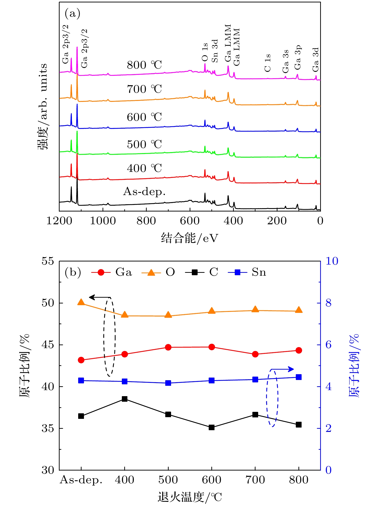
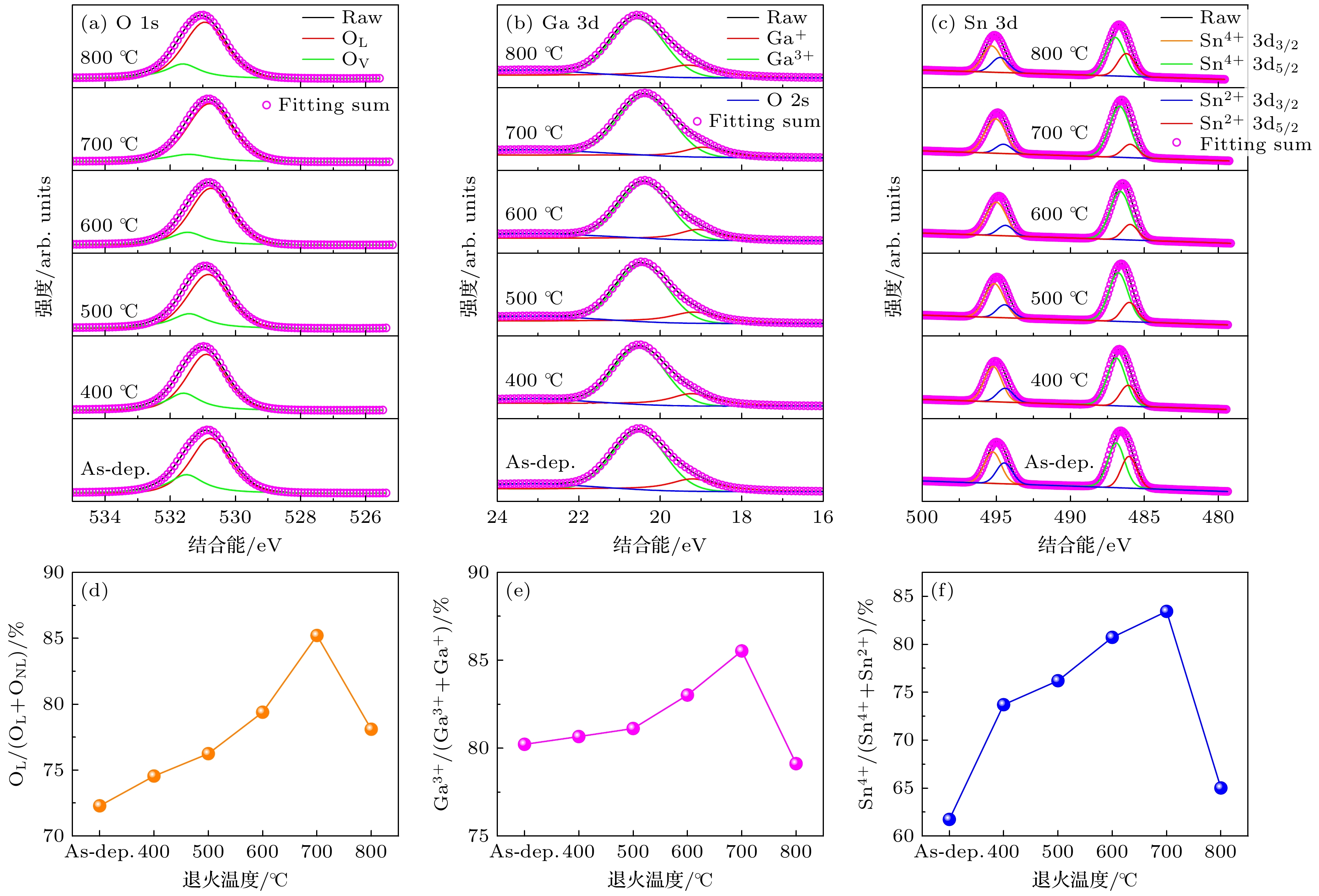
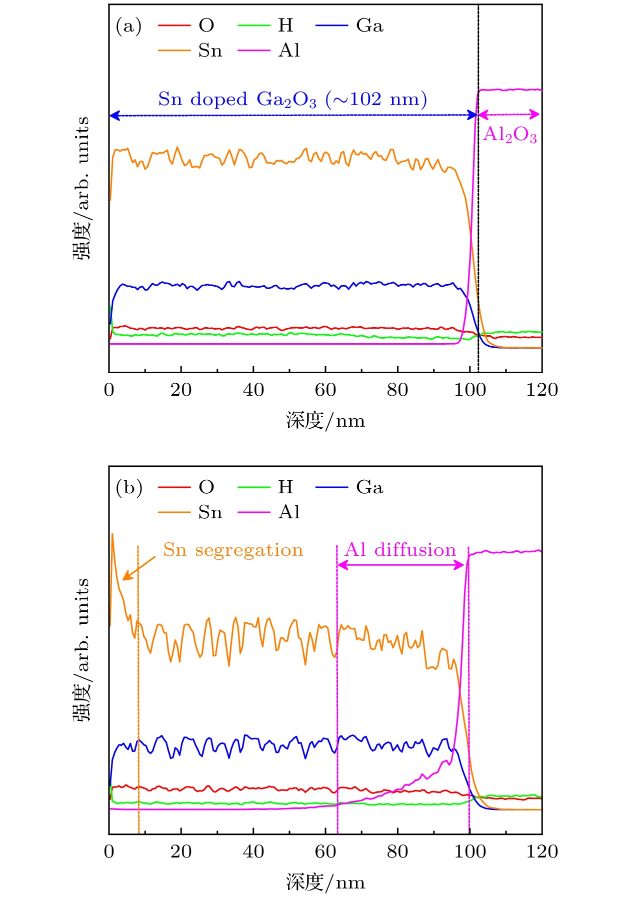
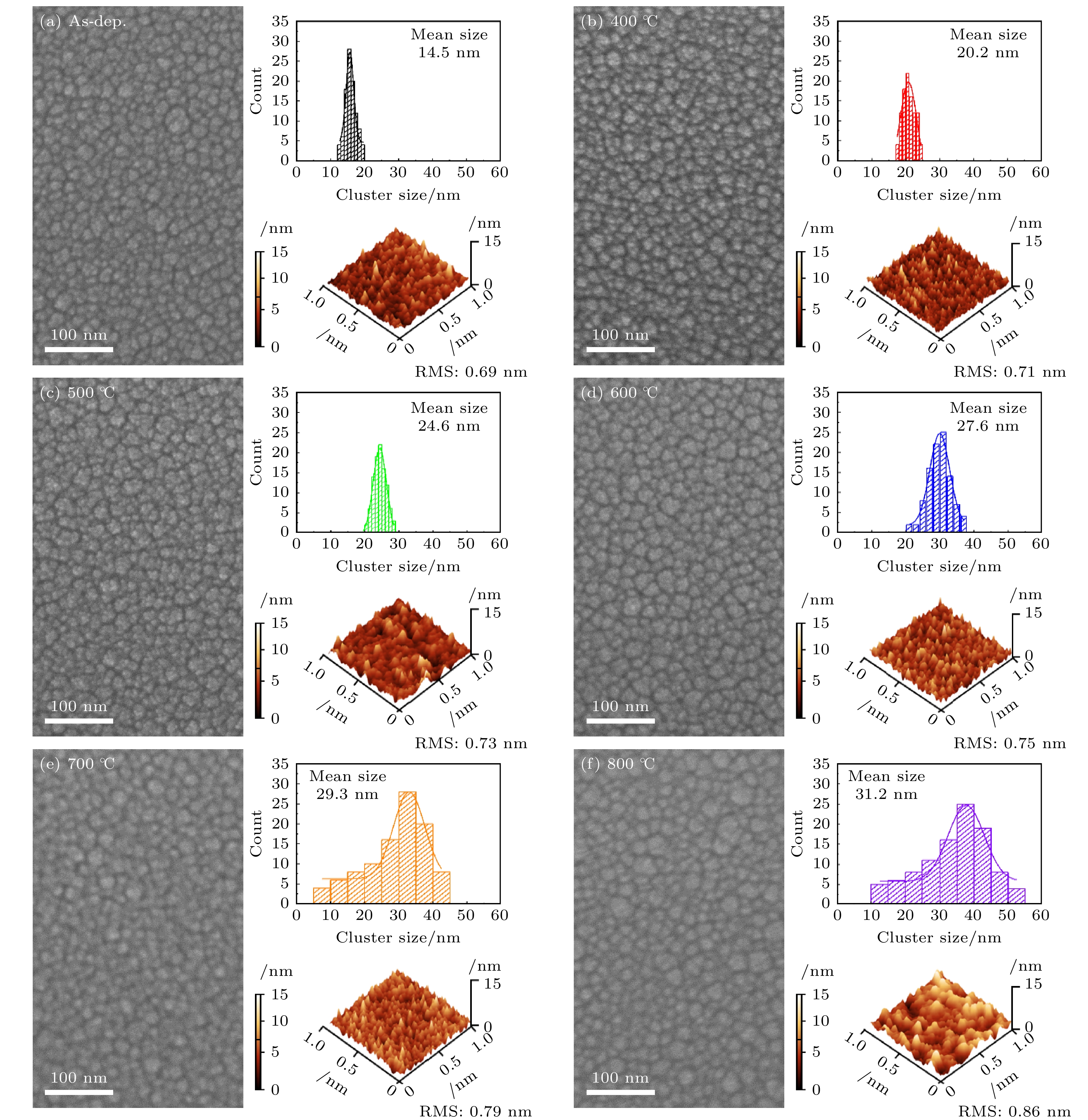
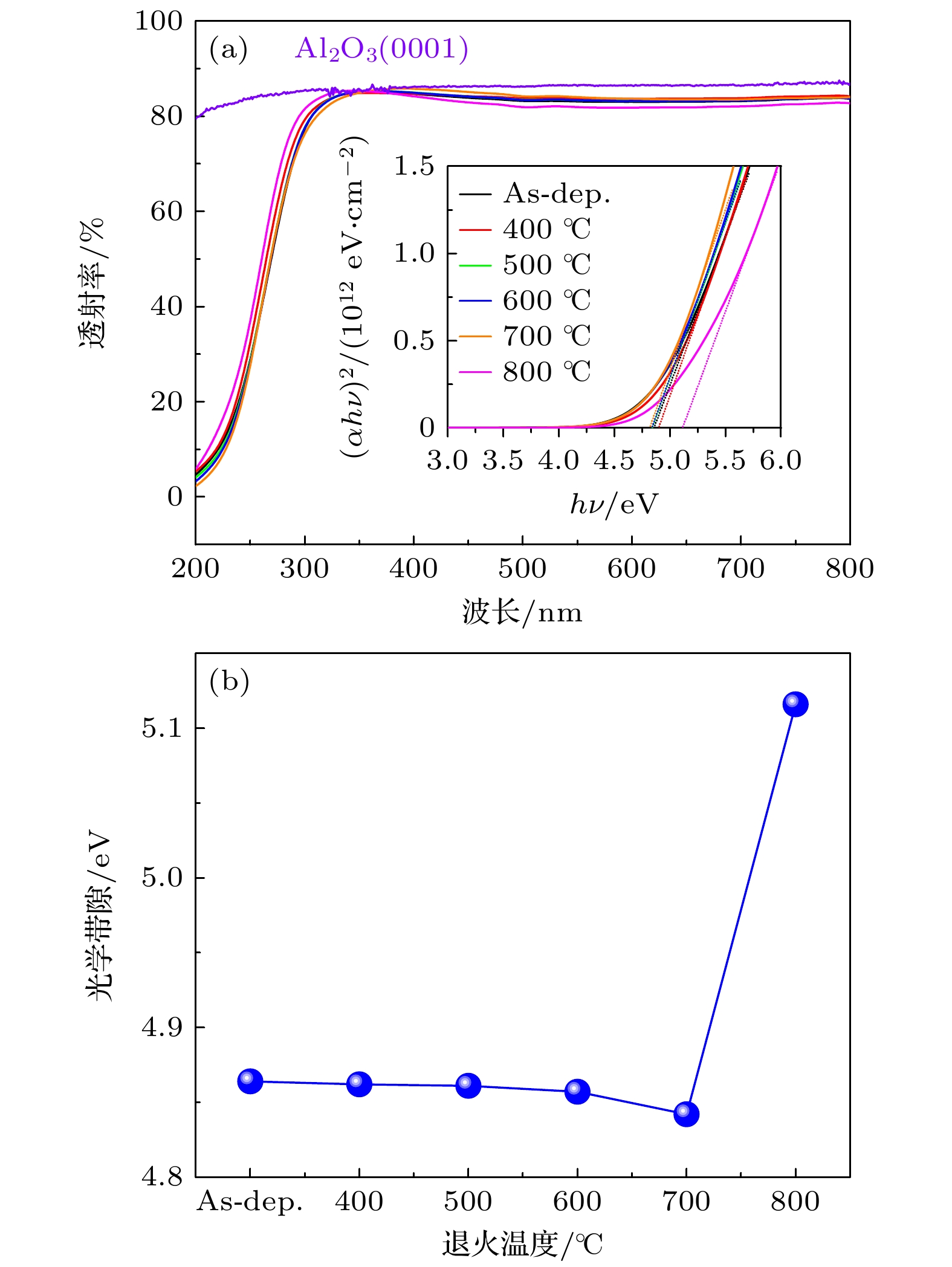
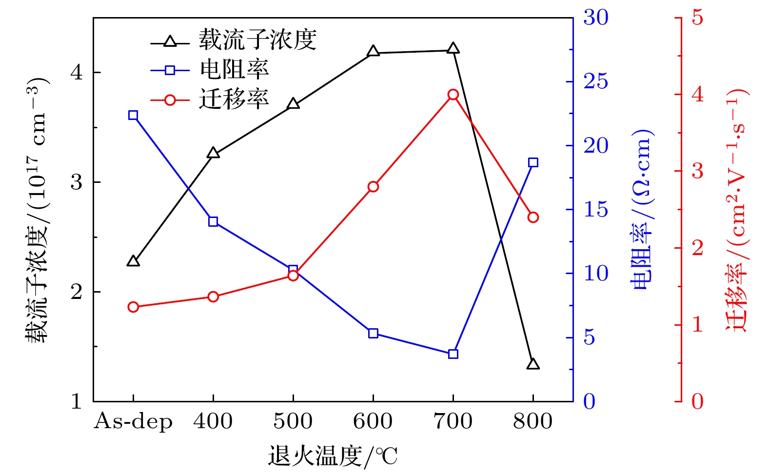
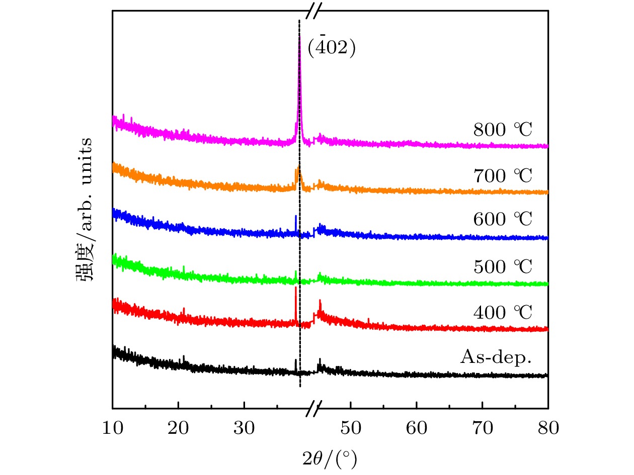
In this study, Sn-doped Ga2O3 thin films are prepared on sapphire substrate by radio frequency magnetron sputtering at ambient temperature, and then annealed at different temperatures (400–800 ℃) in nitrogen atmosphere. The corresponding metal-semiconductor-metal (MSM) solar blind photodetectors (PDs) are prepared based on those films before and after annealing to explore the influence of annealing temperature on the characteristics of the films and device properties. The results show that the as-deposited Sn-doped Ga2O3 film displays amorphous structure. With the increase of annealing temperature, the proportion of OL, Ga3+ and Sn4+ ions in the film increase, and the band gap of the film decreases slightly, indicating that the conductivity of the film is enhanced and the quality of the film is improved. When the annealing temperature increases to 700 ℃, the β-Ga2O3 (${\bar 402} $) crystal surface diffraction peak appeares, indicating that the film begins to crystallize. As the annealing temperature increases to 800 ℃, the proportion of OL, Ga3+ and Sn4+ decreases, and the quality and conductive properties of the film deteriorate, which may be attributed to Sn surface segregation and Al diffusion into the film from the substrate. In addition, the average particle size and surface roughness of the film surface increase with annealing temperature increasing, which is consistent with the changing trend of film characteristics. Then, based on Sn-doped Ga2O3 thin films before and after annealing, the MSM solar blind PDs are prepared to explore the influence of annealing temperature on device performance. The quality of the film and its conductive characteristics play a role in regulating the performance of Sn-doped Ga2O3 solar blind PD. The optimal device performance can be obtained when the annealing temperature is 700 ℃, with a low dark current of 89.97 pA, a responsivity of 18.4 mA/W, a light-dark current up to 1264, and the rise/fall time of 0.93 s/0.87 s. In summary, the annealing temperature has an important effect on the characteristics of Sn-doped Ga2O3 films and the performance of solar blind PDs, which has certain guiding significance for the preparation of high-quality Sn-doped Ga2O3 films and high-performance solar blind PDs.
-
Keywords:
- radio frequency magnetron sputtering /
- Sn-doped Ga2O3 film /
- annealing temperature /
- solar-blind photodetector
[1] Pearton S, Yang J, Cary IV P H, Ren F, Kim J, Tadjer M J, Mastro M A 2018 Appl. Phys. Express 5 011301
[2] Wang C, Fan W H, Cao R J, et al. 2024 Vacuum 225 113246
 Google Scholar
[3] Zhang Y J, Yan J L, Zhao G, Xie W F 2010 Physica B 405 3899
 Google Scholar
[4] Kudou J, Funasaki S, Takahara M, et al. 2012 Materials Science Forum. Trans Tech Publications Ltd 725 269
[5] Vega E, Isukapati S B, Oder T N 2021 J. Vac. Sci. Technol. A 39 033412
 Google Scholar
[6] Lee S Y, Kang H C 2018 Jpn. J. Appl. Phys. 57 01AE02
 Google Scholar
[7] Li L J, Li C K, Wang S Q, Lu Q, Jia Y F, Chen H F 2023 J. Semicond. 44 062805
 Google Scholar
[8] 王尘, 张宇超, 范伟航, 李世韦, 张小英, 林海军, 连水养, 朱文章 2022 光学学报 42 0831001
 Google Scholar
Wang C, Zhang Y C, Fan W H, Li S W, Zhang X Y, Lin H J, Lien S Y, Zhu W Z 2022 Acta Opt. Sin. 42 0831001
 Google Scholar
[9] Dorneles L S, O’Mahony D, Fitzgerald C B, McGee F, Venkatesan M, Stanca I, Lunney J G, Coey J M D 2005 Appl. Surf. Sci. 248 406
 Google Scholar
[10] Schurig P, Couturier M, Becker M, Polity A, Klar P J 2019 Phys. Status Solidi A. 216 1900385
 Google Scholar
[11] Wu J W, Mi W, Yang Z C, Chen Y T, Li P J, Zhao J S, Zhang K L, Zhang X C, Luan C B 2019 Vacuum 167 6
 Google Scholar
[12] Joshi G, Chauhan Y S, Verma A 2021 J. Alloy. Compd. 883 160799
 Google Scholar
[13] Wang C, Li S W, Zhang Y C, Fan W H, Lin H J, Wuu D S, Lien S Y, Zhu W Z 2022 Vacuum 202 111176
 Google Scholar
[14] Zhao X L, Cui W, Wu Z P, Guo D Y, Li P G, An Y H, Li L H, Tang W H 2017 J. Electronic Mater. 46 2366
 Google Scholar
[15] Spencer J A, Mock A L, Jacobs A G, Schubert M, Zhang Y H, Tadjer M J 2022 Appl. Phys. Rev. 9 011315
 Google Scholar
[16] Khan A F, Mehmood M, Rana A M, Bhatti M T 2009 Appl. Surf. Sci. 255 8562
 Google Scholar
[17] Ghose S, Rahman S, Hong L, Rojas-Ramirez J S, Jin H, Park K, Klie R, Droopad R 2017 J. Appl. Phys. 122 095302
 Google Scholar
[18] Qian L X, Liu H Y, Zhang H F, Wu Z H, Zhang W L 2019 Appl. Phys. Lett. 114 113506
 Google Scholar
[19] Zhang J, Shi J, Qi D C, Chen L, Zhang K H L 2020 APL Mater. 8 020906
 Google Scholar
[20] Blumenschein N, Kadlec C, Romanyuk O, Paskova T, Muth J F, Kadlec F 2020 J. Appl. Phys. 127 165702
 Google Scholar
[21] Singh R, Lenka T R, Panda D K, et al. 2020 Mat. Sci. Semicon. Proc. 119 105216
 Google Scholar
[22] Nie Y Y, Jiao S J, Meng F X, Lu H L, Wang D B, Li L, Gao S Y, Wang J Z, Wang X H 2019 J. Alloy. Compd. 798 568
 Google Scholar
[23] Kuznetsov M V, Safonov A V 2023 Mater. Chem. Phys. 302 127739
 Google Scholar
[24] Jubu P R, Yam F K, Igba V M, Beh K P 2020 J. Solid State Chem. 290 121576
 Google Scholar
[25] Gutierrez G, Sundin E M, Nalam P G, et al. 2021 J. Phys. Chem. C 125 20468
 Google Scholar
[26] Korhonen E, Tuomisto F, Bierwagen O, Speck J S, Galazka Z 2014 Phys. Rev. B 90 245307
 Google Scholar
-
图 3 Sn掺杂Ga2O3薄膜退火前后的XPS核心能谱图 (a) O 1s, (b) Ga 3d, (c) Sn 3d; (d)晶格氧OL/(OL+ONL)的比例; (e) Ga3+/(Ga3++Ga+)比例; (f) Sn4+/(Sn4++Sn2+)比例
Figure 3. High-resolution XPS spectra and its fitting spectra of (a) O 1s, (b) Ga 3d, and (c) Sn 3d; the OL proportion (d), Ga3+ ratio (e) and Sn4+ percentage (f) of the films annealed at various temperatures.
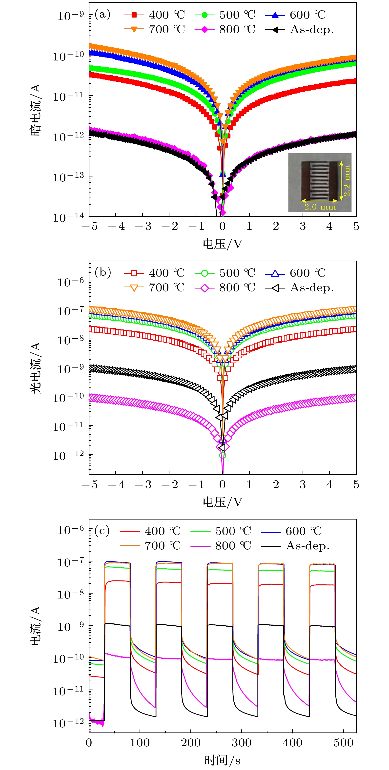
图 8 不同退火温度下Sn掺杂Ga2O3日盲光电探测器 (a) 暗电流, 插图为光学显微镜下器件的俯视图; (b) 光电流; (c) 瞬态响应
Figure 8. (a) The dark current-voltage curves, the inset is the physical top-view of photodetectors; (b) the photocurrent–voltage curves; (c) the transient response (I-t) curves of photodetectors under different annealing temperature.
表 1 磁控溅射Sn掺杂Ga2O3薄膜工艺及退火参数
Table 1. Growth and annealing parameters of the sputtered Sn-doped Ga2O3 films.
参数 值 背景压力/Torr 5×10⁻⁷ 工作压力/Torr 9×10⁻³ 溅射功率/W 500 气体总流量/SCCM 40 氧流量比[O2/(O2+Ar)]/% 1.0 沉积温度/℃ 室温 薄膜厚度/nm ~102 退火气氛和时间 N2气体和2 h 退火温度/℃ As-dep., 400, 500, 600, 700, 800 注: SCCM为体积流量单位(standard cubic centimeter per minute). 表 2 退火前后Sn掺杂Ga2O3探测器的性能参数
Table 2. Performance of the Sn-doped Ga2O photodetectors before and after annealing.
退火温度/℃ 暗电流/pA 光电流/nA 光暗>电流比 响应度/(mA·W–1) 上升时间/s 下降时间/s As-dep. 1.10 0.94 854.5 0.15 1.61 1.02 400 23.33 22.05 945.14 3.57 2.28 3.54 500 63.85 66.73 1045.11 10.8 1.43 1.34 600 80.28 89.65 1116.72 14.5 1.03 0.98 700 89.97 113.74 1264.20 18.4 0.93 0.87 800 1.14 0.09 82.46 0.02 1.12 17.36 -
[1] Pearton S, Yang J, Cary IV P H, Ren F, Kim J, Tadjer M J, Mastro M A 2018 Appl. Phys. Express 5 011301
[2] Wang C, Fan W H, Cao R J, et al. 2024 Vacuum 225 113246
 Google Scholar
[3] Zhang Y J, Yan J L, Zhao G, Xie W F 2010 Physica B 405 3899
 Google Scholar
[4] Kudou J, Funasaki S, Takahara M, et al. 2012 Materials Science Forum. Trans Tech Publications Ltd 725 269
[5] Vega E, Isukapati S B, Oder T N 2021 J. Vac. Sci. Technol. A 39 033412
 Google Scholar
[6] Lee S Y, Kang H C 2018 Jpn. J. Appl. Phys. 57 01AE02
 Google Scholar
[7] Li L J, Li C K, Wang S Q, Lu Q, Jia Y F, Chen H F 2023 J. Semicond. 44 062805
 Google Scholar
[8] 王尘, 张宇超, 范伟航, 李世韦, 张小英, 林海军, 连水养, 朱文章 2022 光学学报 42 0831001
 Google Scholar
Wang C, Zhang Y C, Fan W H, Li S W, Zhang X Y, Lin H J, Lien S Y, Zhu W Z 2022 Acta Opt. Sin. 42 0831001
 Google Scholar
[9] Dorneles L S, O’Mahony D, Fitzgerald C B, McGee F, Venkatesan M, Stanca I, Lunney J G, Coey J M D 2005 Appl. Surf. Sci. 248 406
 Google Scholar
[10] Schurig P, Couturier M, Becker M, Polity A, Klar P J 2019 Phys. Status Solidi A. 216 1900385
 Google Scholar
[11] Wu J W, Mi W, Yang Z C, Chen Y T, Li P J, Zhao J S, Zhang K L, Zhang X C, Luan C B 2019 Vacuum 167 6
 Google Scholar
[12] Joshi G, Chauhan Y S, Verma A 2021 J. Alloy. Compd. 883 160799
 Google Scholar
[13] Wang C, Li S W, Zhang Y C, Fan W H, Lin H J, Wuu D S, Lien S Y, Zhu W Z 2022 Vacuum 202 111176
 Google Scholar
[14] Zhao X L, Cui W, Wu Z P, Guo D Y, Li P G, An Y H, Li L H, Tang W H 2017 J. Electronic Mater. 46 2366
 Google Scholar
[15] Spencer J A, Mock A L, Jacobs A G, Schubert M, Zhang Y H, Tadjer M J 2022 Appl. Phys. Rev. 9 011315
 Google Scholar
[16] Khan A F, Mehmood M, Rana A M, Bhatti M T 2009 Appl. Surf. Sci. 255 8562
 Google Scholar
[17] Ghose S, Rahman S, Hong L, Rojas-Ramirez J S, Jin H, Park K, Klie R, Droopad R 2017 J. Appl. Phys. 122 095302
 Google Scholar
[18] Qian L X, Liu H Y, Zhang H F, Wu Z H, Zhang W L 2019 Appl. Phys. Lett. 114 113506
 Google Scholar
[19] Zhang J, Shi J, Qi D C, Chen L, Zhang K H L 2020 APL Mater. 8 020906
 Google Scholar
[20] Blumenschein N, Kadlec C, Romanyuk O, Paskova T, Muth J F, Kadlec F 2020 J. Appl. Phys. 127 165702
 Google Scholar
[21] Singh R, Lenka T R, Panda D K, et al. 2020 Mat. Sci. Semicon. Proc. 119 105216
 Google Scholar
[22] Nie Y Y, Jiao S J, Meng F X, Lu H L, Wang D B, Li L, Gao S Y, Wang J Z, Wang X H 2019 J. Alloy. Compd. 798 568
 Google Scholar
[23] Kuznetsov M V, Safonov A V 2023 Mater. Chem. Phys. 302 127739
 Google Scholar
[24] Jubu P R, Yam F K, Igba V M, Beh K P 2020 J. Solid State Chem. 290 121576
 Google Scholar
[25] Gutierrez G, Sundin E M, Nalam P G, et al. 2021 J. Phys. Chem. C 125 20468
 Google Scholar
[26] Korhonen E, Tuomisto F, Bierwagen O, Speck J S, Galazka Z 2014 Phys. Rev. B 90 245307
 Google Scholar
Catalog
Metrics
- Abstract views: 3479
- PDF Downloads: 294
- Cited By: 0


 DownLoad:
