


-
Through-silicon via (TSV), as a key technology for realizing interconnections in three-dimensional integrated circuits (3D ICs), critically depends on the integrity of its sidewall interfaces to maintain optimal leakage characteristics. In this work, the temperature cycling experiments, incorporating leakage current I-V testing, microstructural observations are conducted, and the EDS elemental analysis is made to evaluate the effects of temperature cycling on the integrity of TSV sidewall interfaces and the leakage mechanisms in the insulation layer. The results indicate that as the number of temperature cycles increases, the alternating cyclic loads progressively degrade the integrity of the TSV barrier layer, transitioning from an intact interface to the formation of micro-voids and micro-cracks, which results in a significant increase in leakage current. When through-thickness cracks appear at the interface, a sudden decrease in leakage current occurs. The TSV failure mode is transforms from thermally induced leakage to mechanical cracking. The leakage mechanism of the insulation layer transforms from the Schottky emission mechanism (Cycle≤60) into a combination of Schottky emission and Poole-Frenkel emission mechanisms (Cycle≥90), and this transformation becomes more pronounced under high electric field conditions. Further analysis of TSV interface integrity reveals that thermomechanical stress induced by temperature cycling generates defects at the interface between the TSV copper fill and the barrier layer. As thermally induced defects accumulate, the barrier height of the insulation layer continuously decreases, making it easier for electrons in the metal to overcome the Schottky barrier under thermal and electric field excitation, thereby forming leakage currents. Moreover, these defects facilitate the diffusion of copper atoms into the insulation layer, thereby forming localized high electric field regions. These high-field regions in the insulation layer increase electron emission rates through the Poole-Frenkel emission mechanism, creating leakage paths. Therefore, copper diffusion emerges as one of the primary causes of dielectric performance degradation in the insulation layer.
-
Keywords:
- through silicon via /
- leakage mechanism /
- temperature cycling
[1] Wang Y K, Liu H Z, Huo L H, Li H B, Tian W C, Ji H Y, Chen S 2024 Micromachines 15 422
 Google Scholar
[2] Jang Y J, Sharma A, Jung J P 2023 Materials 16 7652
Google Scholar
[3] 董刚, 武文珊, 杨银堂 2015 物理学报 64 026601
Google Scholar
Dong G, Wu W S, Yang Y T 2015 Acta Phys. Sin. 64 026601
Google Scholar
[4] 董刚, 刘荡, 石涛, 杨银堂 2015 物理学报 64 176601
Google Scholar
Dong G, Liu D, Shi T, Yang Y T 2015 Acta Phys. Sin. 64 176601
Google Scholar
[5] Fan Z W, Chen X, Wang Y S, Jiang Y, Zhang S F 2022 Microelectron. Reliab. 138 114643
Google Scholar
[6] Kumari V, Chandrakar S, Verma S, Majumder M K 2023 IEEE Trans. Compon. Packag. Manuf. Technol. 13 1734
Google Scholar
[7] Chan J M, Lee K C, Tan C S 2018 IEEE Trans. Device Mater. Reliab. 18 520
Google Scholar
[8] Chan J M, Cheng X, Lee K C, Kanert W, Tan C S 2017 IEEE International Reliability Physics Symposium (IRPS) Monterey, CA, April 2–6, 2017 p4A
[9] Chandrakar M, Majumder M K 2022 IEEE Trans. Compon. Packag. Manuf. Technol. 12 1832
Google Scholar
[10] Gong T, Xie L L, Chen S, Lu X J, Zhao M R, Zhu J Y, Yang X F, Wang Z Z 2024 Crystals 14 37
[11] Shen Z S, Jing S Y, Heng Y Y, Yao Y F, Tu K N, Liu Y X 2023 Appl. Phys. Rev. 10 021309
Google Scholar
[12] Nakamura T, Kitada H, Mizushima Y, Maeda N, Fujimoto K, Ohba T 2012 IEEE 2011 International 3D Systems Integration Conference (3DIC) Osaka, Japan, January 31– February 2, 2012 p1
[13] Ranganathan N, Lee D Y, Youhe L, Lo G Q, Prasad K, Pey K L 2011 IEEE Trans. Compon. Packag. Manuf. Technol. 1 1497
Google Scholar
[14] Lin Y, Tan C S 2018 Jpn. J. Appl. Phys. 57 07MF01
Google Scholar
[15] Chen S, Jian X D, Li K, Li G Y, Wang Z Z, Yang X F, Wang H Y, Fu Z W 2023 Microelectron. Reliab. 141 114889
Google Scholar
[16] Hung J F, Lau J H, Chen P S, Wu S H, Lai S J, Li M L, Sheu S S, Tzeng P J, Lin Z H, Ku T K, Lo W C, Kao M J 2012 IEEE 62nd Electronic Components and Technology Conference(ECTC) San Diego, CA, May 29–June 1, 2012 p564
[17] Krause M, Altmann F, Schmidt C, Petzold M, Malta D, Temple D 2011 IEEE 61st Electronic Components and Technology Conference (ECTC) Lake Buena Vista, FL, May 31–June 3, 2011 p1452
[18] Chiu F C 2014 Adv. Mater. Sci. Eng. 2014 578168
Google Scholar
[19] Fowler R H, Nordheim L 1928 Proc. R. Soc. London, Ser. A 119 173
Google Scholar
[20] Frenkel J 1938 Phys. Rev. 54 647
Google Scholar
[21] Schottky W 1939 Z. Phys. 113 367
Google Scholar
-
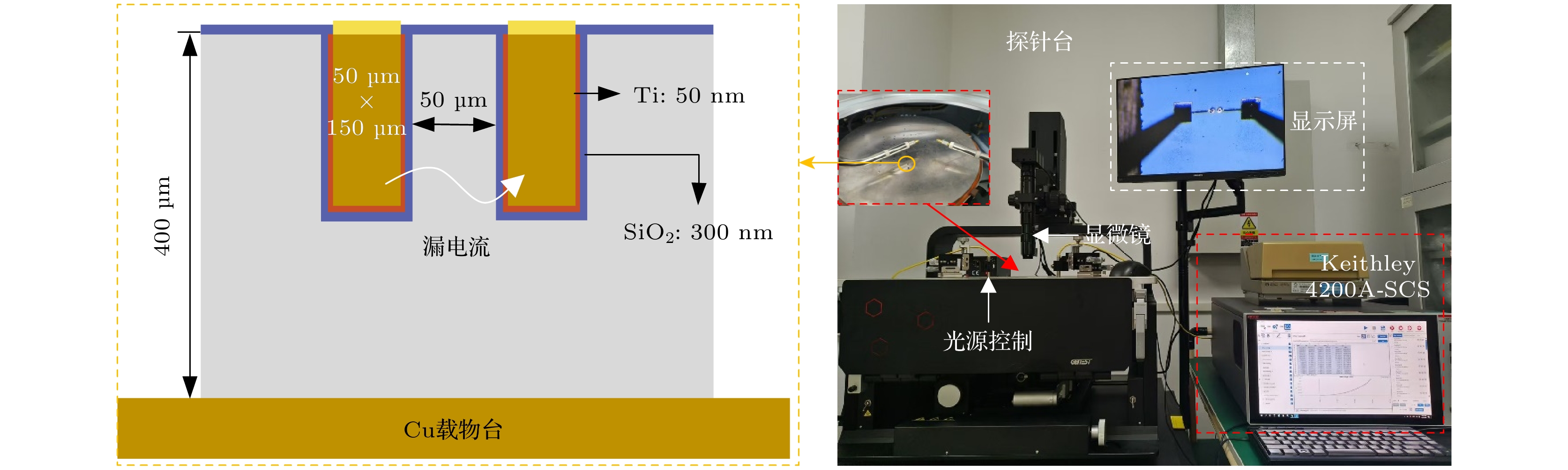
图 1 测试平台及样品介绍
Figure 1. Test platform and sample introduction.
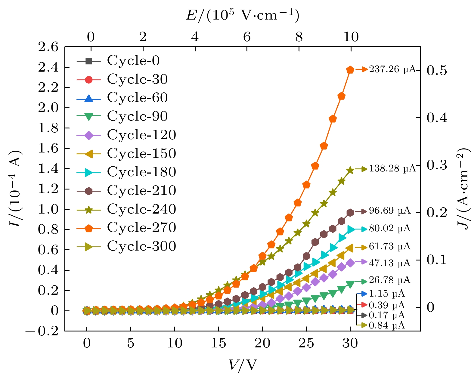
图 2 0—300次温度循环样品I-V (J-E )测试结果
Figure 2. I-V (J-E ) test results of samples after 0–300 temperature cycles.
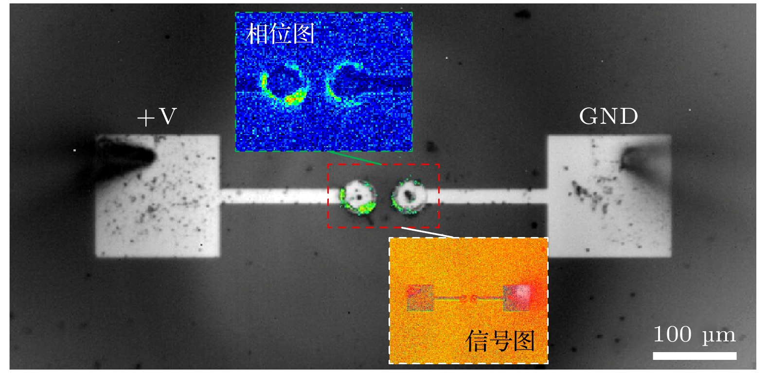
图 3 LIT定位TSV侧壁缺陷结果图
Figure 3. LIT detection results of TSV sidewall defects.
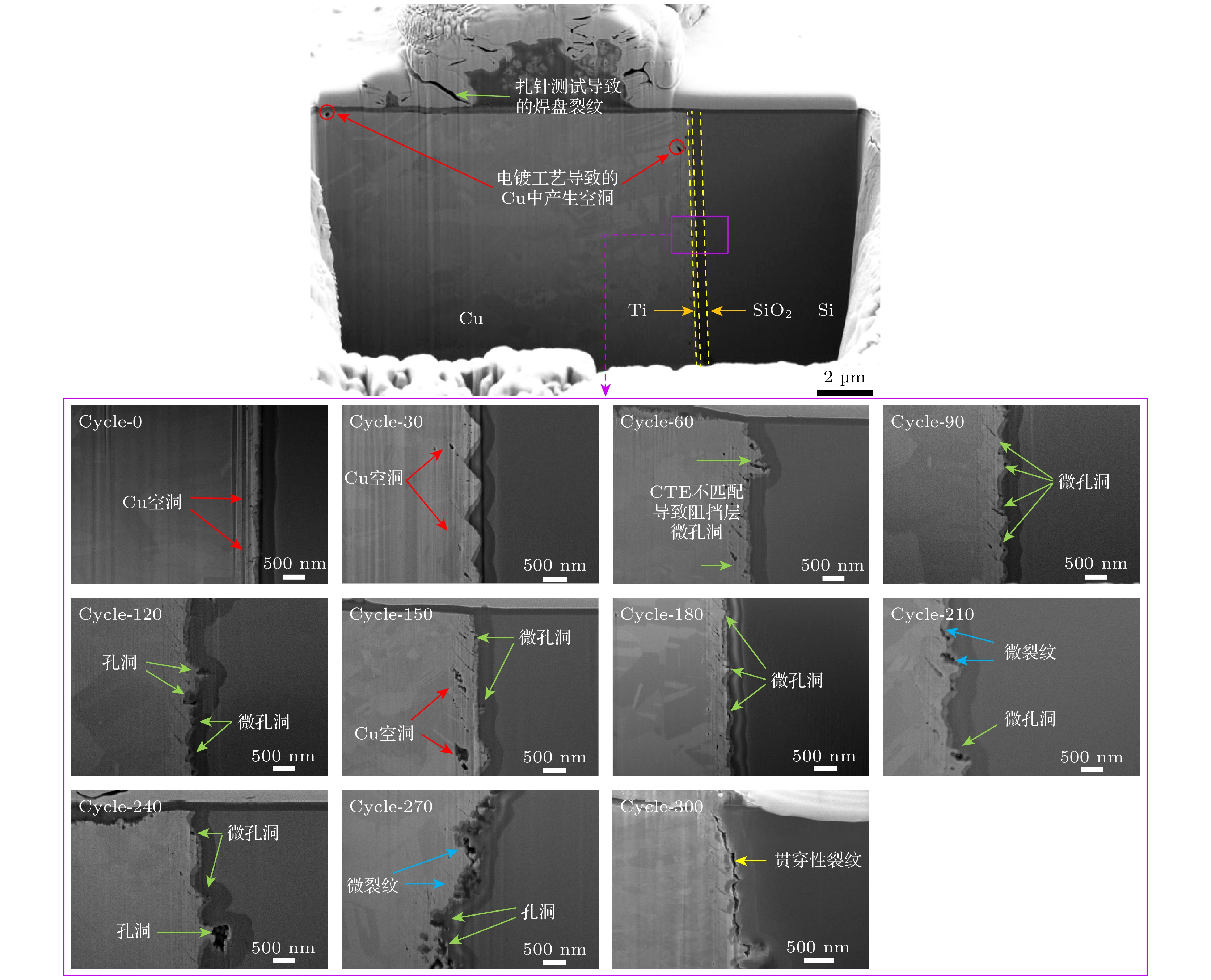
图 4 不同温度循环次数下TSV界面微观结构图
Figure 4. Microstructure of TSV interfaces under different temperature cycling numbers.
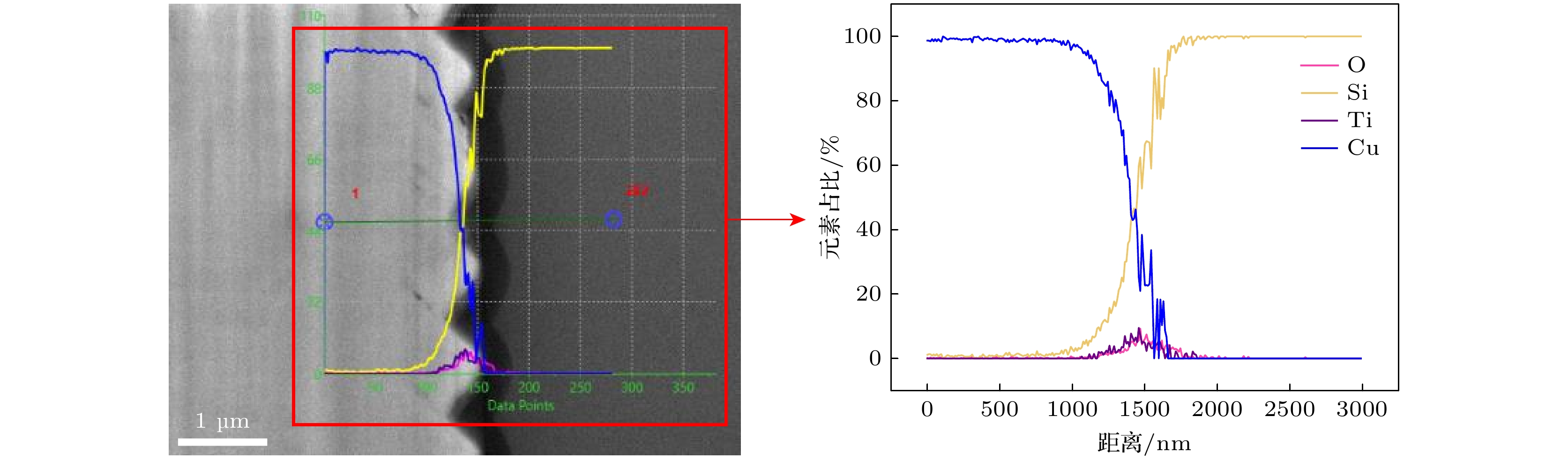
图 5 Cycle-30 EDS元素分析结果图
Figure 5. Results of cycle-30 EDS elemental analysis.
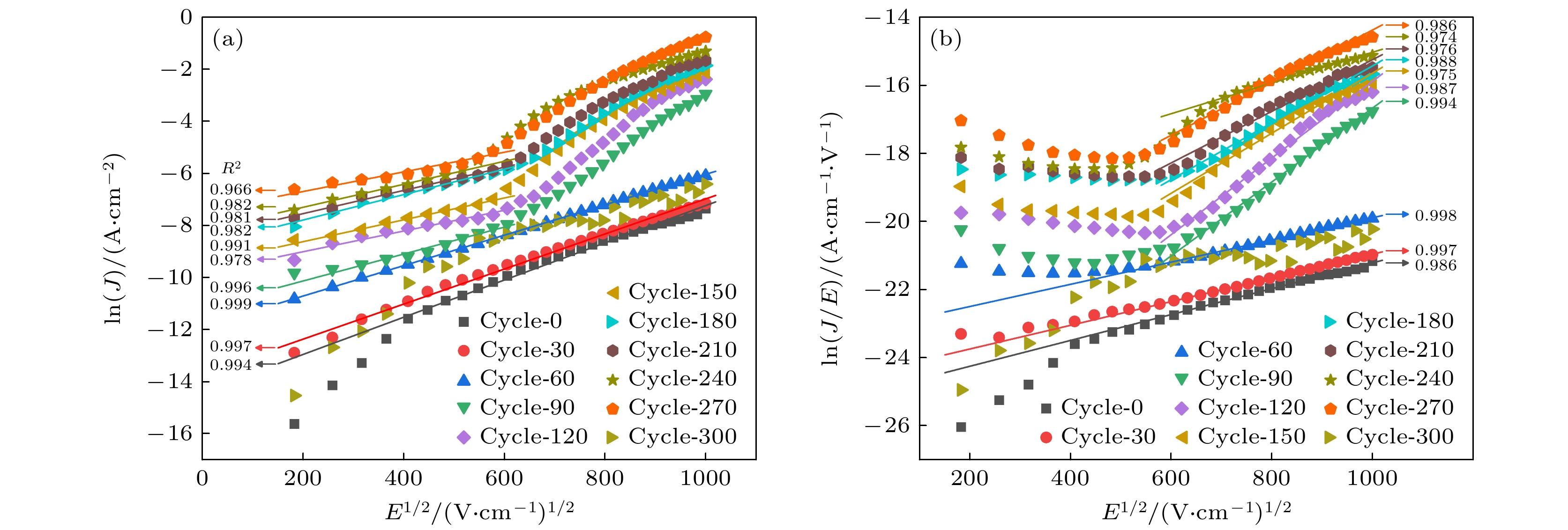
图 6 漏电机制拟合曲线 (a) 肖特基拟合; (b) P-F拟合
Figure 6. Leakage current mechanism fitting curves: (a) Schottky fitting; (b) P-F fitting.
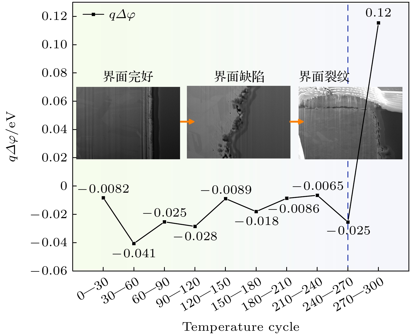
图 7 不同温度循环次数后绝缘层势垒高度变化值
Figure 7. Variation in insulation layer barrier height after different numbers of temperature cycles.
表 1 不同温度循环次数下绝缘层中Cu元素比例
Table 1. Cu element proportion in insulation layer under different temperature cycling numbers.
温循次数 0 30 60 90 120 150 180 210 240 270 300 Cu质量含量/% 9.19 9.22 12.55 18.07 27.44 33.59 37.16 41.98 44.19 48.29 15.85  DownLoad: CSV
表 2 漏电机制模型
Table 2. Leakage mechanism models.
漏电机制 理论公式 拟合公式 参数说明 P-F发射 $ {J_{{\text{F-P}}}} = CE\exp \left( {\dfrac{{ - {\varphi _{\text{t}}} + q\sqrt {qE/4{\text{π}}{\varepsilon _0}{\varepsilon _{\text{r}}}} }}{{kT}}} \right) $ $ \mathrm{ln}\left(J_{\text{F-P}}/E\right)=A_{{\text{F-P}}}\sqrt{E}+B_{{\text{F-P}}} $ J 为电流密度
q 为电子电荷
E为电场强度
φt 为势陷深度
ε0 为真空介电常数
εr 为介电常数肖特基发射 ${J_{\text{S}}} = A{T^2}\exp \left( {\dfrac{{ - {\varphi _{\text{s}}} + q\sqrt {qE/4{\text{π}}{\varepsilon _0}{\varepsilon _{\text{r}}}} }}{{kT}}} \right)$ $ \mathrm{ln}J_{\text{S}}=A_{\text{S}}\sqrt{E}+B_{\text{S}} $ A 为有效理查德森常数
T 为绝对温度
φs 为肖特基势垒高度
k 为玻尔兹曼常数
DownLoad: CSV
-
[1] Wang Y K, Liu H Z, Huo L H, Li H B, Tian W C, Ji H Y, Chen S 2024 Micromachines 15 422
Google Scholar
[2] Jang Y J, Sharma A, Jung J P 2023 Materials 16 7652
Google Scholar
[3] 董刚, 武文珊, 杨银堂 2015 物理学报 64 026601
Google Scholar
Dong G, Wu W S, Yang Y T 2015 Acta Phys. Sin. 64 026601
Google Scholar
[4] 董刚, 刘荡, 石涛, 杨银堂 2015 物理学报 64 176601
Google Scholar
Dong G, Liu D, Shi T, Yang Y T 2015 Acta Phys. Sin. 64 176601
Google Scholar
[5] Fan Z W, Chen X, Wang Y S, Jiang Y, Zhang S F 2022 Microelectron. Reliab. 138 114643
Google Scholar
[6] Kumari V, Chandrakar S, Verma S, Majumder M K 2023 IEEE Trans. Compon. Packag. Manuf. Technol. 13 1734
Google Scholar
[7] Chan J M, Lee K C, Tan C S 2018 IEEE Trans. Device Mater. Reliab. 18 520
Google Scholar
[8] Chan J M, Cheng X, Lee K C, Kanert W, Tan C S 2017 IEEE International Reliability Physics Symposium (IRPS) Monterey, CA, April 2–6, 2017 p4A
[9] Chandrakar M, Majumder M K 2022 IEEE Trans. Compon. Packag. Manuf. Technol. 12 1832
Google Scholar
[10] Gong T, Xie L L, Chen S, Lu X J, Zhao M R, Zhu J Y, Yang X F, Wang Z Z 2024 Crystals 14 37
[11] Shen Z S, Jing S Y, Heng Y Y, Yao Y F, Tu K N, Liu Y X 2023 Appl. Phys. Rev. 10 021309
Google Scholar
[12] Nakamura T, Kitada H, Mizushima Y, Maeda N, Fujimoto K, Ohba T 2012 IEEE 2011 International 3D Systems Integration Conference (3DIC) Osaka, Japan, January 31– February 2, 2012 p1
[13] Ranganathan N, Lee D Y, Youhe L, Lo G Q, Prasad K, Pey K L 2011 IEEE Trans. Compon. Packag. Manuf. Technol. 1 1497
Google Scholar
[14] Lin Y, Tan C S 2018 Jpn. J. Appl. Phys. 57 07MF01
Google Scholar
[15] Chen S, Jian X D, Li K, Li G Y, Wang Z Z, Yang X F, Wang H Y, Fu Z W 2023 Microelectron. Reliab. 141 114889
Google Scholar
[16] Hung J F, Lau J H, Chen P S, Wu S H, Lai S J, Li M L, Sheu S S, Tzeng P J, Lin Z H, Ku T K, Lo W C, Kao M J 2012 IEEE 62nd Electronic Components and Technology Conference(ECTC) San Diego, CA, May 29–June 1, 2012 p564
[17] Krause M, Altmann F, Schmidt C, Petzold M, Malta D, Temple D 2011 IEEE 61st Electronic Components and Technology Conference (ECTC) Lake Buena Vista, FL, May 31–June 3, 2011 p1452
[18] Chiu F C 2014 Adv. Mater. Sci. Eng. 2014 578168
Google Scholar
[19] Fowler R H, Nordheim L 1928 Proc. R. Soc. London, Ser. A 119 173
Google Scholar
[20] Frenkel J 1938 Phys. Rev. 54 647
Google Scholar
[21] Schottky W 1939 Z. Phys. 113 367
Google Scholar

 DownLoad:
Catalog
Metrics
- Abstract views: 2748
- PDF Downloads: 129
- Cited By: 0
