SPECIAL TOPIC—Plasmon-enhanced light-matter interactions
2019, 68 (14): 147302.
doi: 10.7498/aps.68.20190802
Abstract +
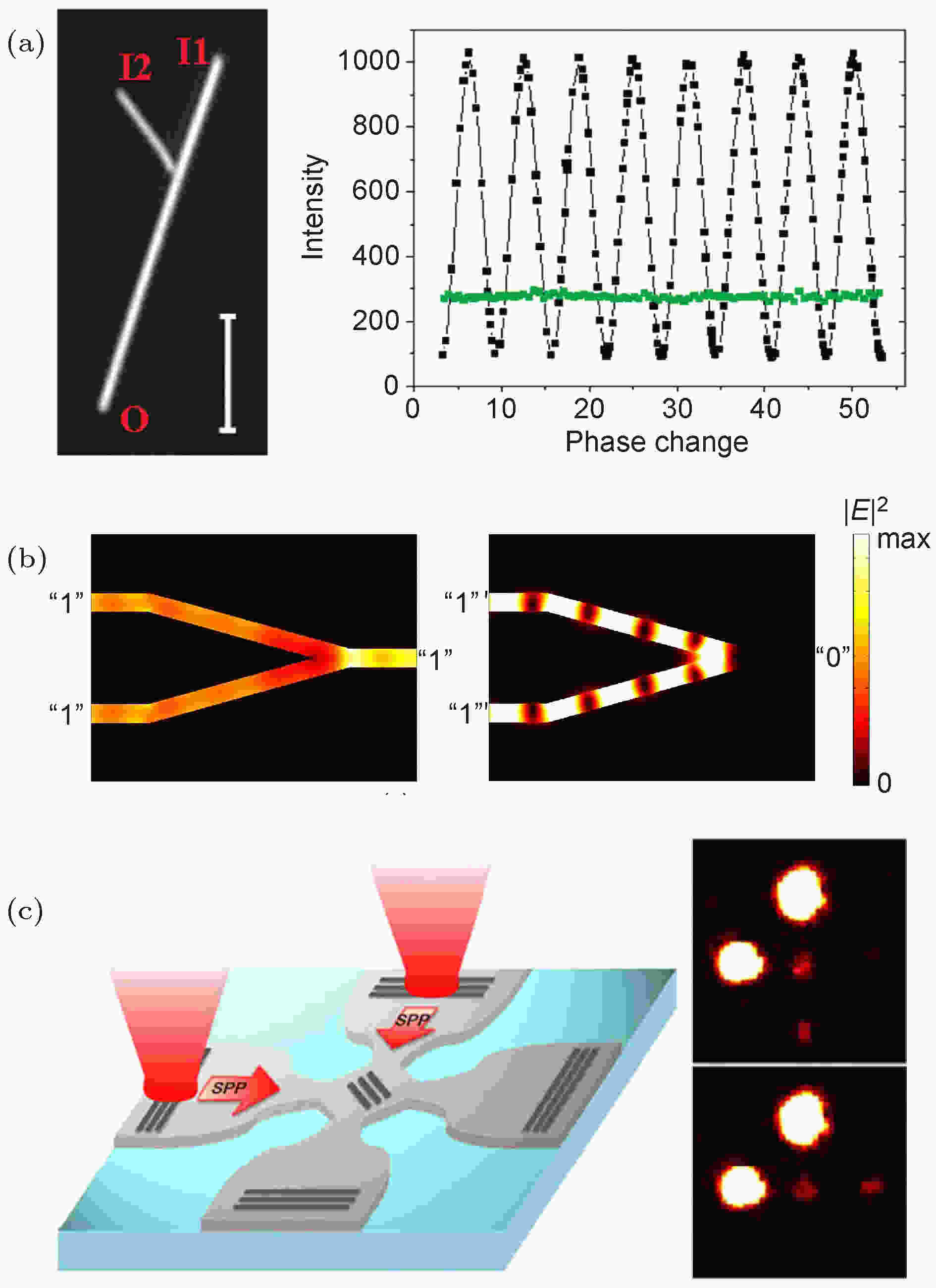
The diffraction limit of light greatly limits the development of conventional optical devices, which are difficult to be miniaturized and integrated with high density. Surface plasmons, electromagnetic modes at the metal-dielectric interface, can concentrate light into deep subwavelength dimensions, enabling the manipulation of light at the nanometer scale. Surface plasmons can be used as information carrier to transmit and process optical signals beyond the diffraction limit. Therefore, nanodevices based on surface plasmons have received much attention. By modulating surface plasmons, the modulation of optical signals at nanoscale can be realized, which is important for the development of on-chip integrated nanophotonic circuits and optical information technology. In this article, we review the modulations of propagating surface plasmons and their applications in nano-optical modulators. The wave vector of propagating surface plasmons is very sensitive to the dielectric function of the metal and the environment. By tuning the dielectric function of the metal and/or the surrounding medium, both the real and imaginary part of the wave vector of surface plasmons can be modified, leading to the modulation of the phase and propagation length of surface plasmons and thereby modulating the intensity of optical signals. We first introduce the basic principles of different types of modulations, including all-optical modulation, thermal modulation, electrical modulation, and magnetic modulation. The all-optical modulation can be achieved by modulating the polarization and phase of input light, pumping optical materials, changing the dielectric function of metal by control light, and manipulating a nanoparticle by optical force to modulate the scattering of surface plasmons. The modulation based on thermal effect depends on thermo-optic materials and phase-change materials, and the temperature change can be triggered by photothermal effect or electrical heating. For electrically controlled modulation, Pockels electro-optic effect and Kerr electro-optic effect can be employed. Electrical modulation can also be realized by controlling the carrier concentration of semiconductors or graphene, using electrochromatic materials, and nanoelectromechanical control of the waveguide. The modulation of surface plasmons by magnetic field relies on magneto-optic materials. We review recent research progresses of modulating propagating surface plasmons by these methods, and analyze the performances of different types of plasmonic modulators, including operation wavelength, modulation depth or extinction ratio, response time or modulation frequency, and insertion loss. Finally, a brief conclusion and outlook is presented.

2019, 68 (14): 144101.
doi: 10.7498/aps.68.20190606
Abstract +
The localized surface plasmons in metal nanostructures under optical excitation will lead to near-field localization and enhancement, which have shown important applications in surface enhancement spectroscopy, ultra-sensitive sensing, microfluidic chip, enhanced optical force, etc. The plasmon resonance and the resulting electric field enhancement strongly depend on wavelength and structure geometry. As a result, the optical force will be closely related to the field distribution, that is, the optical force can be used to manipulate and sort plasmonic metal structures. The large near-field enhancement and gradient of metal nanoparticle aggregates can also be used as a " plasmonic tweezer” to manipulate other particles. Furthermore, in the case of changing the incident polarization and even for a new type of structured laser beam, the optical manipulation has a higher degree of freedom. In this review, having briefly introduced the plasmon-enhanced optical force, we focus on the recent advances in the following three aspects: 1) the manipulation of plasmonic nanoparticles by optical tweezer, 2) the manipulation of other particles by plasmonic tweezer, and 3) dependence of plasmonic optical force on the polarization, optical angular momentum, structured light and the structured chirality. Comparing with other topics of plasmon- enhanced light-interactions, there is plenty of room for further developing the plasmon-enhanced optical force and optical manipulation. Several research trends can be foreseen. 1) More precise optical manipulating and sorting of nanoparticles (even sub-nanometer). For example, more sensitive special resonant modes (e.g. Fano resonance) of plasmonic nanostructure can be utilized. For some nanostructures with small feature sizes, especially when the gap size is close to 1 nm, the non-local effect has a certain effect on the plasmon resonance. Therefore, when calculating the optical force in this case, non-local effects and possibly other quantum effects should be considered. 2) Richer laser fields, that is, using various new structured fields and chiral structures provides a higher degree of freedom for the optical forces and optical manipulation. Also, the localized surface plasmons can be combined with propagating surface plasmons. 3) Wider applications of plasmonic optical forces, especially in combination with other effects and even interdiscipline, e.g. enhanced spectroscopy, enhanced single particle chemical reactions, nonlinear optical effects, and photothermal manipulations.
2019, 68 (14): 144201.
doi: 10.7498/aps.68.20190269
Abstract +
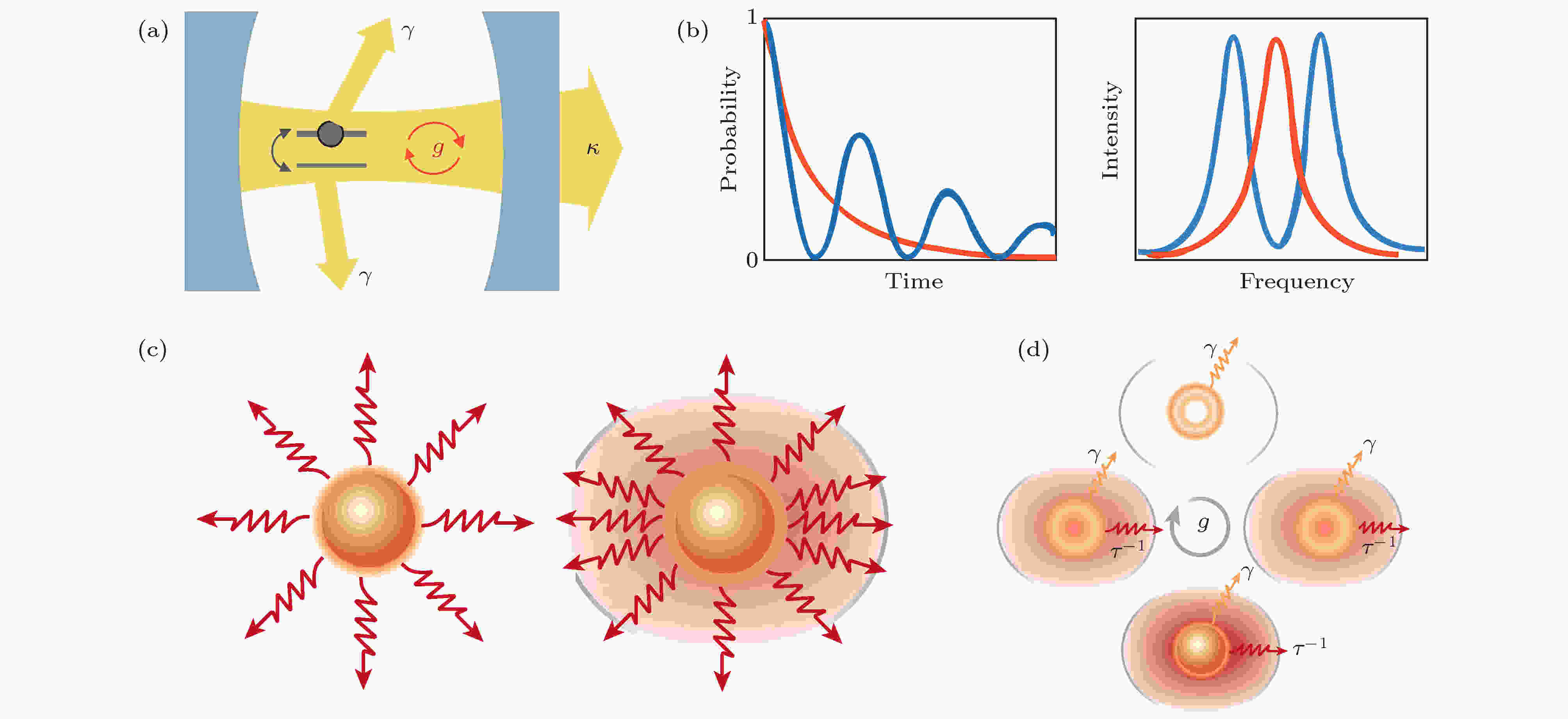
The strong localized field in micro-nano photonic structures brings new opportunities for the study of the light-matter interaction. By designing optical modes in these structures, photons and excitons in micro-nanostructures can exchange energy reversibly or irreversibly. In this paper, a series of our recent studies on the strong and weak photon-emitter coupling in micro-nano structures especially in plasmonic and their coupled structures are reviewed, such as the principle of efficient, tunable and directional single photon emission, and engineering the electromagnetic vacuum for enhancing the coupling between photon and exciton. These results provide new physical contents for the light-matter interactions on micro and nanoscale, and have potential applications in the on-chip quantum information process and the construction of scalable quantum networks.

2019, 68 (14): 144401.
doi: 10.7498/aps.68.20190476
Abstract +
Plasmonic nanostructure can efficiently manipulate light on a subwavelength scale, which can break through the optical diffraction limit and significantly enhance the interaction between light and matter. In the study of photoelectric devices based on the plasmonic mechanism, the absorption of light in surface plasmons is usually considered as loss, which needs to be suppressed. However, based on the photothermal effect, the light absorption of plasmonic nanostructure can be effectively utilized and converted into heat. The research of this new type of nano-heat source is a hot topic in the field of plasmonics. In this paper, we review the recent progress of the study of photothermal effects of plasmonic nanostructure, focusing on the physical process of heating effects, and the methods to control the temperature distribution in both the process of heat generation and the process of delivery of heat. Finally, the applications of nano-heat source in the fields of nano-fabrication and broad-spectrum photothermal conversion are also presented.

2019, 68 (14): 146201.
doi: 10.7498/aps.68.20190564
Abstract +
Surface plasmons (SPs) are the surface waves of collective oscillations of free electrons at metal-dielectric interface, which have the ability to overcome the diffraction limit and to enhance the giant near-field. Tapered metallic nanostructures that support surface plasmons’ propagation are highly attractive to nanophotonic applications because of their waveguiding and field-focusing properties. This distinct morphologic feature enables the functionality known as nanofocusing. As a result, the plasmons can be guided in these nanostructures and finally focused on the sharp apex to greatly enhance the local field. This attractive effect can be widely used for effective remote-excitation detection/sensing. In this paper, we review various types of plasmonic nanofocusing structures operating in the visible and infrared region. We focus on their fundamentals, fabrications, and applications. Firstly, we discuss the mechanisms of the plasmonic nanofocusing. Then, the characteristics of various tapered metallic nanostructures of SPs are reviewed, including on-chip waveguides, metal tips and bottom-up fabricated nanowires. For applications, some prototypes of plasmonic nanofocusing for bio/chemo sensing are demonstrated. Finally, a summary and outlook of plasmonic waveguides are given.
2019, 68 (14): 147102.
doi: 10.7498/aps.68.20190345
Abstract +
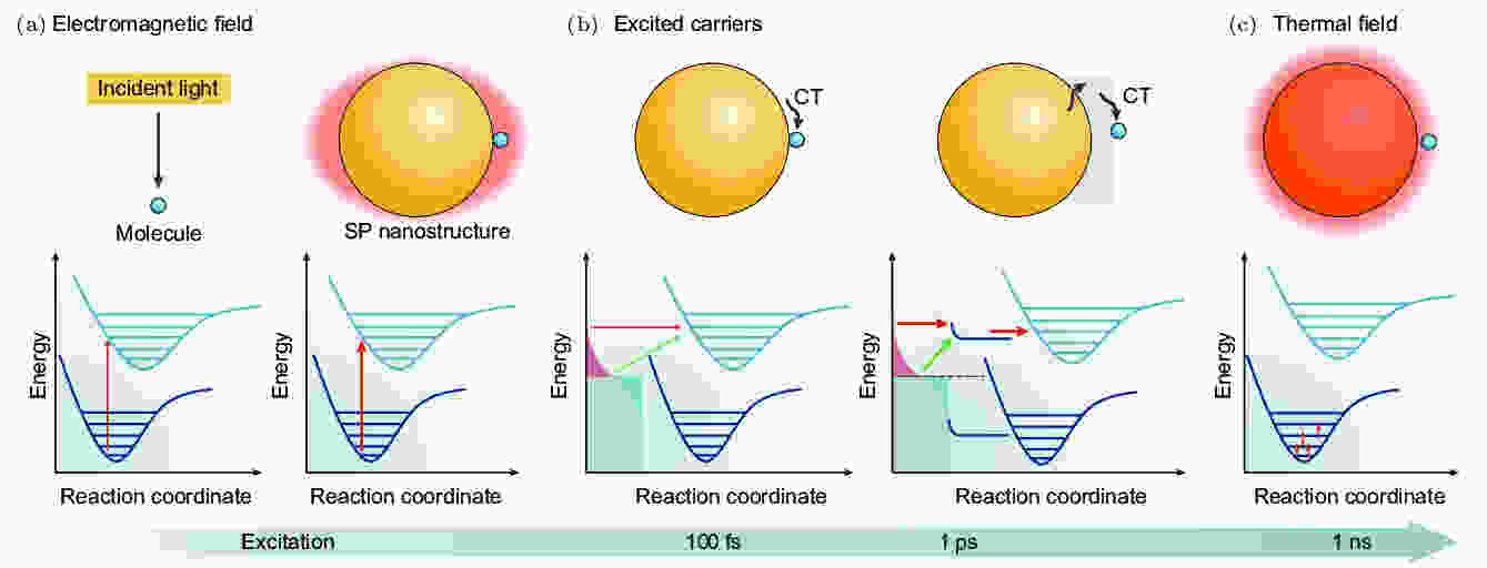
Surface plasmons are collective oscillations of free electrons at the interface between metal and dielectric. Surface plasmons can break through the diffraction limit of light, because the electromagnetic field is confined in a very small space near the surface of the nanostructure, which provides a possibility for nanometer-scale light manipulation. By using surface plasmon resonance, the local surface electromagnetic field can be strongly enhanced, which can be used to enhance the molecular fluorescence and Raman signals. In addition, the plasmon relaxation induces thermal electrons which can drive the catalytic reaction of surface molecules to achieve a selective catalytic reaction at normal temperature, which is so-called plasmon mediated chemical reaction (or plasmonic catalysis). As a new type of catalytic system, plasmonic catalysis can mediate chemical reactions that are difficult to occur under various conventional conditions. Due to the complexity and diversity of plasmon catalyzed reactions, it is still a huge challenge to fully characterize the reaction kinetics and understand its reaction mechanism. Characterizing the intermediate and final products in the catalytic reaction accurately and obtaining more detailed information in the reaction process are essential for exploring the theoretical mechanism of plasmon catalysis. In this paper, we review the characterization techniques used in plasmon catalysis in detail in the progress of plasmon catalysis. First, the basic concepts of plasmon catalysis and several common catalytic mechanisms are introduced. Second, the Raman spectroscopy, including the application of surface and tip-enhanced Raman spectroscopy in plasmon catalytic in situ monitoring are reviewed. Then, the other techniques such as gas chromatography, gas chromatography-mass spectrometry, high performance liquid chromatography, scanning transmission electron microscopy, scanning tunneling microscopy, scanning electrochemical microscopy and UV-visible absorption spectroscopy for monitoring plasmon catalyzed reaction are introduced in detail. Finally, the characteristics and advantages of these characterization techniques in the study of kinetic catalytic process and catalytic mechanism of plasmon, and the future development and challenge are mentioned and analyzed.
2019, 68 (14): 147103.
doi: 10.7498/aps.68.20190331
Abstract +
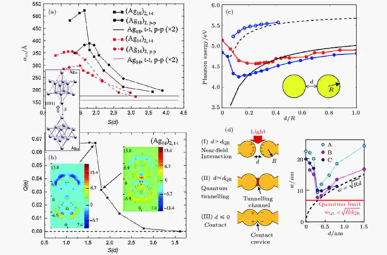
Plasmonics, focusing on the fundamental researches and novel applications of plasmons, has rapidly developed as an important branch of nano-optics in recent years. Essentially, surface plasmons are highly localized collective electron excitation at a metal-dielectric interface. This elementary excitation can be strongly coupled with electromagnetic fields, which enable one to collect, manipulate, and emit micron-scale optical signals through using nano-scale structures. Recently, the quantum properties of plasmons have received tremendous attention as nanofabrication techniques approach to the quantum limit. On this scale, with the unique intrinsic properties of plasmons, i.e. the particle-like nature of photons and wave-like nature of electrons, quantum plasmonics exhibits very attractive prospects in quantum information, high-efficiency optoelectronic devices, and highly sensitive detection, etc. Here in this paper, we review the development of quantum plasmonics in recent years, by introducing the research progress of relevant theories and the experimental breakthroughes. Some perspectives of the future development of quantum plasmonics are also outlined.

COVER ARTICLE
2019, 68 (14): 147104.
doi: 10.7498/aps.68.20190434
Abstract +
Surface plasmons in metallic nanostructures can confine the optical field within the region of subwavelength, even nanometer scale, and thus enhance the light-matter interaction and other physical processes, which will lead the plasmon optics to possess attractive applications in many areas. However, the " mode volume” often used to characterize field confinement in plasmonic structures is only defined phe-nomenologically and suffers ambiguity when applied to complex structures. In this work, we develop a theoretical method to characterize the field confinement based on quasi-normal mode analysis. We recognize the fact that a plasmonic resonance may result from many eigen-modes, which together contribute to the observed field confinement. An effective mode volume is introduced for quasi-normal modes and used to characterize the field confinement when the plasmonic resonance is dominated by a single quasi-normal mode. Two typical kinds of plasmonic structures are systematically examined, and the field confinement on the order of 10 nm3–100 nm3 is confirmed. In pursuit of the ultimate field confinement, we revisit the so-called " pico-cavity” formed by an atomistic protrusion in the nano gap of the particle-on-mirror configuration. The apparent hot spot is shown to have contributions from several quasi-normal modes. The dominant one exhibits a further squeezed mode volume compared with the scenario without the protrusion, but is still well above 10 nm3.
2019, 68 (14): 147301.
doi: 10.7498/aps.68.20190276
Abstract +
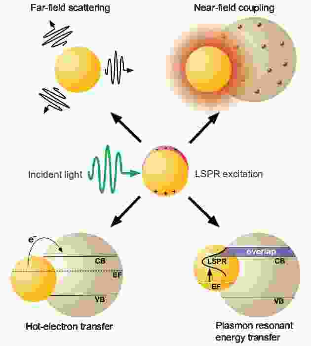
Plasmon resonance energy transfer refers to the coherent energy transfer via dipole-dipole coupling from surface plasmons to adjacent exciton nanosystems such as semiconductor quantum dots or dye molecules. The plasmon resonance energy transfer is a non-radiative plasmon decay pathway, which can also act as an available channel to extract the plasmon-harvested energy. In addition, hot electron relaxation (non-radiative channel) and scattering (radiative channel) are also the dissipation pathways of surface plasmon resonances. The plasmon-harvested energy can be effectively transferred to other nanosystems or converted into other energy forms through these correlated dissipation pathways. In this paper, the underlying mechanism and dynamics of the plasmon resonance energy transfer as well as the related energy and charge transfer processes (such as near field enhancement and coupling, far field scattering, plasmon-induced hot electron transfer) are introduced. The recent research progress of the plasmon-enhanced photocatalysis by energy and charge transfer is reviewed.
2019, 68 (14): 147303.
doi: 10.7498/aps.68.20190469
Abstract +
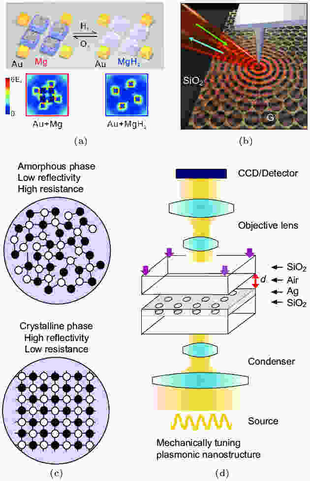
As is well known, plasmonics bridges the gap between nanoscale electronics and dielectric photonics, and is expected to be applied to light generation, photonic integration and chips, optical sensing and nanofabrication technology. So far, most of plasmonic microstructures and nanostructures cannot dynamically tune the properties once their structures are fabricated. Therefore, developing active plasmonic materials and devices is especially desired and necessary. Recently, dynamically tunable plasmonic materials and devices have been intensively investigated with the aim of practical applications. Here in this paper, we review recent research advances in active plasmonic materials and devices. Firstly we summarize three approaches to dynamically tuning plasmonic materials and devices. The first approach is to dynamically change the effective permittivity of metallic microstructures and nanostructures. The second approach is to dynamically adjust the ambient environments of the materials and devices. The third approach is to real-time tune the coupling effects in the nanostructures. Then we take ordinary plasmonic materials, plasmonic metamaterials, and plasmonic metasurfaces for example to show how to make them dynamically tunable. With external fields (such as electrical field, light field, thermal field, and mechanical force field, etc.), various approaches have been demonstrated in dynamically tuning the physical properties of plasmonic systems in real time. We anticipate that this review will promote the further development of new-generation subwavelength materials and optoelectrionic devices with new principles and better performances.
2019, 68 (14): 147304.
doi: 10.7498/aps.68.20190782
Abstract +
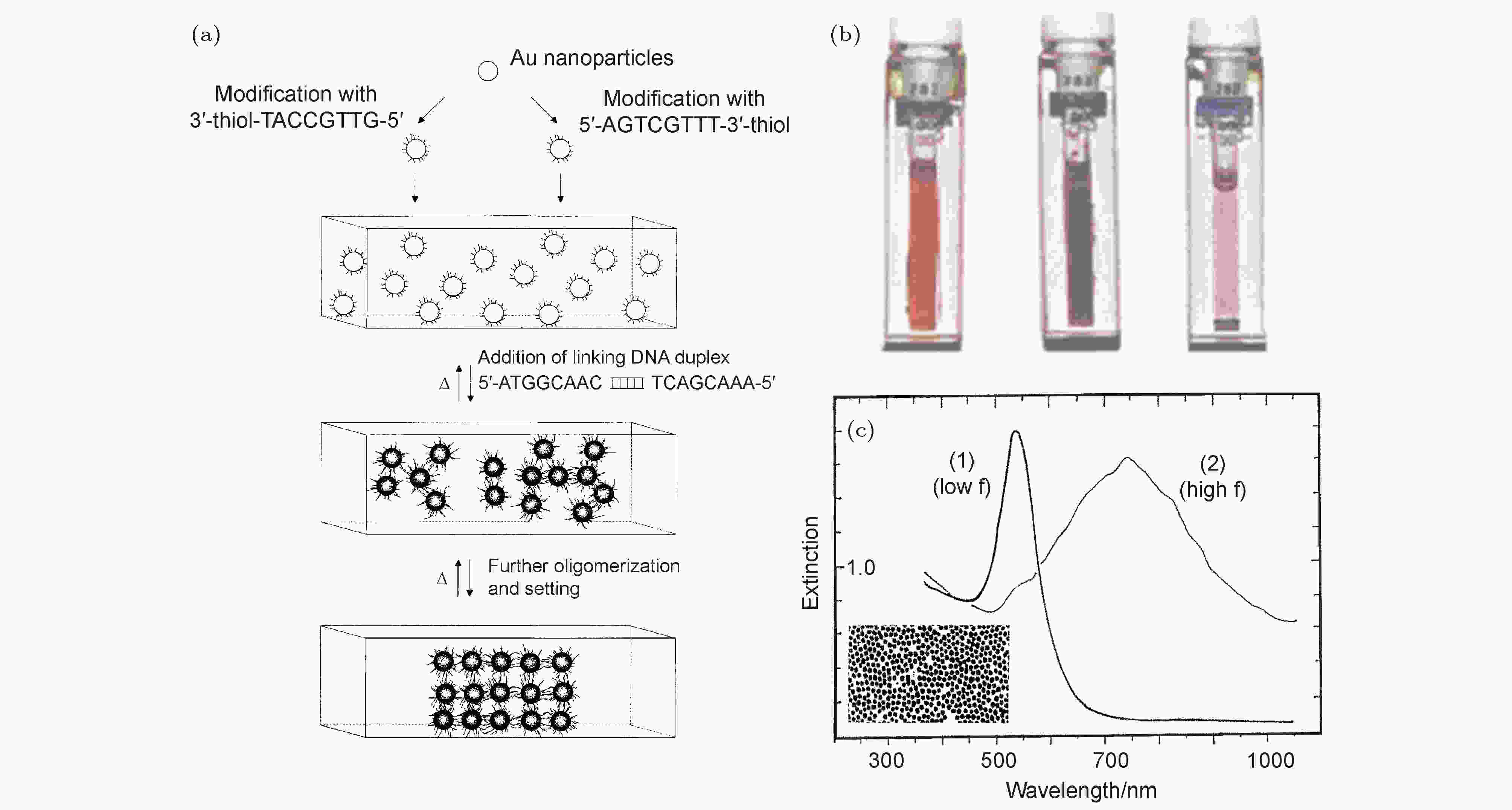
Surface plasmon polariton is a surface oscillation wave that is bound at the interface between metal and dielectric material. Its oscillating electric field is strongly bound below the subwavelength scale near the interface, generating a huge enhancement of localized electromagnetic field, which can be used to greatly enhance the interaction between light and matter, particularly in metal surface plasmon coupling system. In this paper, we review the coupling effects, coupling theory, and typical coupling structures of the surface plasmon coupling systems. We also introduce a typical surface plasmon coupling system and its corresponding crucial applications in surface enhanced refractive index sensor, Raman scattering, near-infrared absorption, and nonlinear effect generation.
EDITOR'S SUGGESTION
2019, 68 (14): 147401.
doi: 10.7498/aps.68.20190458
Abstract +
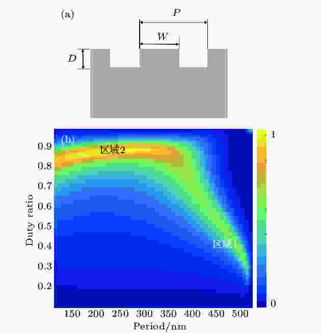
Surface-enhanced Raman scattering (SERS) makes the Raman signals, as fingerprints of different vibration modes of chemical bonds, significant in practical applications. Two main mechanisms, chemical and physical, are attributed to the SERS of molecules adsorbed on metals. The physical mechanism plays a major role in SERS, which is the focus of our paper. Recent SERS systems are mostly based on dimer structures, i.e. nanoparticle pairs, of noble metals. Large amplification of electrical field occurs in the gap of a dimer structure compared with a single nanoparticle. The above gap positions are called as " hot spots” of SERS. In addition, the reproducibility and reliability of SERS substrates are also important for practical applications. Here we use periodical subwavelength metallic structures to meet such needs, and develop other kinds of electrical field enhancement mechanisms. We present the electrical field enhancement of the band-edge mode of surface plasmon polariton, gap plasmon polariton mode, as well as their coupling mode. We choose one-dimensional subwavelength metallic structures to clarify the physical mechanism. Our purpose is to develop subwavelength metallic structures with even and intensive " hot spots”, serving as ultrasensitive solid-state SERS substrates with excellent reproducibility and reliability.
2019, 68 (14): 147801.
doi: 10.7498/aps.68.20190305
Abstract +
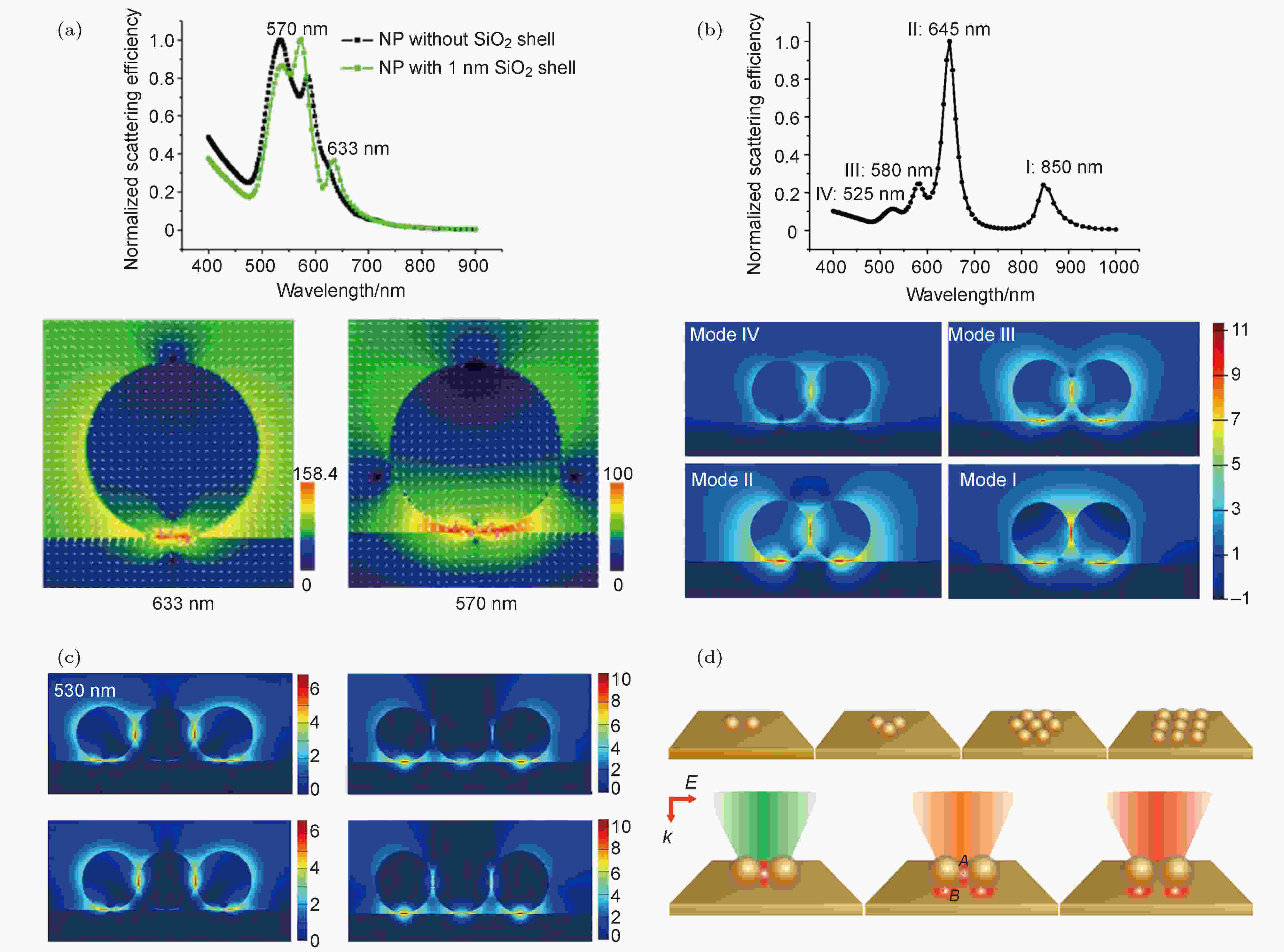
Optical excitations and mutual couplings of surface plasmons with specific modes in metal nanostructures are the physical basis for developing the high spatial resolution, high sensitivity, and high precision spectroscopy. Here, we systematically review latest advances in optical excitations, classifications and identifications of surface plasmon resonance modes and their typical applications in several typical interfaces. We discuss several aspects below. First, the intrinsic mechanism of creating " hot spots” in metal particle-film systems is elucidated by the finite-difference time-domain numerical method. Spatial transfers and influence factors of the " hot spots” under plasmon-induced electric- resonance and plasmon-induced magnetic-resonance conditions are discussed. Second, the plasmon-induced magnetic-resonance in the visible-light region is successfully realized in a gold nanoparticle-film system. Meanwhile, experimental results of surface-enhanced Raman spectroscopy show that the " hot spots” in the magnetic-resonance mode can output Raman scattering with a much higher enhancement factor than that in the conventional electric-resonance mode. Third, we design nonlinear nanorulers that can reach approximately 1-nm resolution by utilizing the mechanism of plasmon-enhanced second-harmonic generation (PESHG). Through introducing Au@SiO2 (core@shell) shell isolated nanoparticles, we strive to maneuver electric-field-related gap modes such that a reliable relationship between PESHG responses and gap sizes, represented by " PESHG nanoruler equation”, can be obtained. Fourth, a critical and general solution is proposed to quantitatively describe the spatial resolution and directional emission in tip-enhanced Raman spectroscopy and tip-enhanced fluorescence. These results may help enhance our understanding of the intrinsic physical mechanism of the surface plasmon resonance, and offer opportunities for potential applications in surface-enhanced Raman spectroscopy, tip-enhanced Raman spectroscopy, second harmonic generation, and other plasmon-enhanced spectroscopy.

2019, 68 (14): 147802.
doi: 10.7498/aps.68.20190702
Abstract +
When light passes through an interface between two media with different refractive indices, part of light energy is reflected and thus causes an inevitable optical reflection. Optical anti-reflection is of great importance for applications in a wide range such as solar cells, optical lenses, infrared sensors, and photo-detectors, which has long been a research topic in the fields of optical systems and optoelectronic devices. In this article, the recent research progress of the optical anti-reflection based on subwavelength artificial engineering materials is reviewed. Having made a brief review of conventional anti-reflection methods, we focus on the overview of the newly developed techniques for optical anti-reflection, such as eliminating reflection by exciting the localized surface plasmons, the enhancement of transmission induced by the excitation of propagating surface plasmons, making metals transparent by the help of metamaterials, and the reduction of anti-reflection in long wavelength infrared and terahertz spectral ranges by using metasurfaces. Compared with the conventional anti-reflection methods, the new technique usually does not suffer the limitation of material, and it benefits from enhanced light absorption and wide incidence angle response. The new technique also enables the design of anti-reflection over wide or a multiple wavelength band. Finally, the future opportunities and challenges for further developing the subwavelength artificial engineering microstructures in optical anti-reflection are also predicted.
2019, 68 (14): 148103.
doi: 10.7498/aps.68.20190903
Abstract +
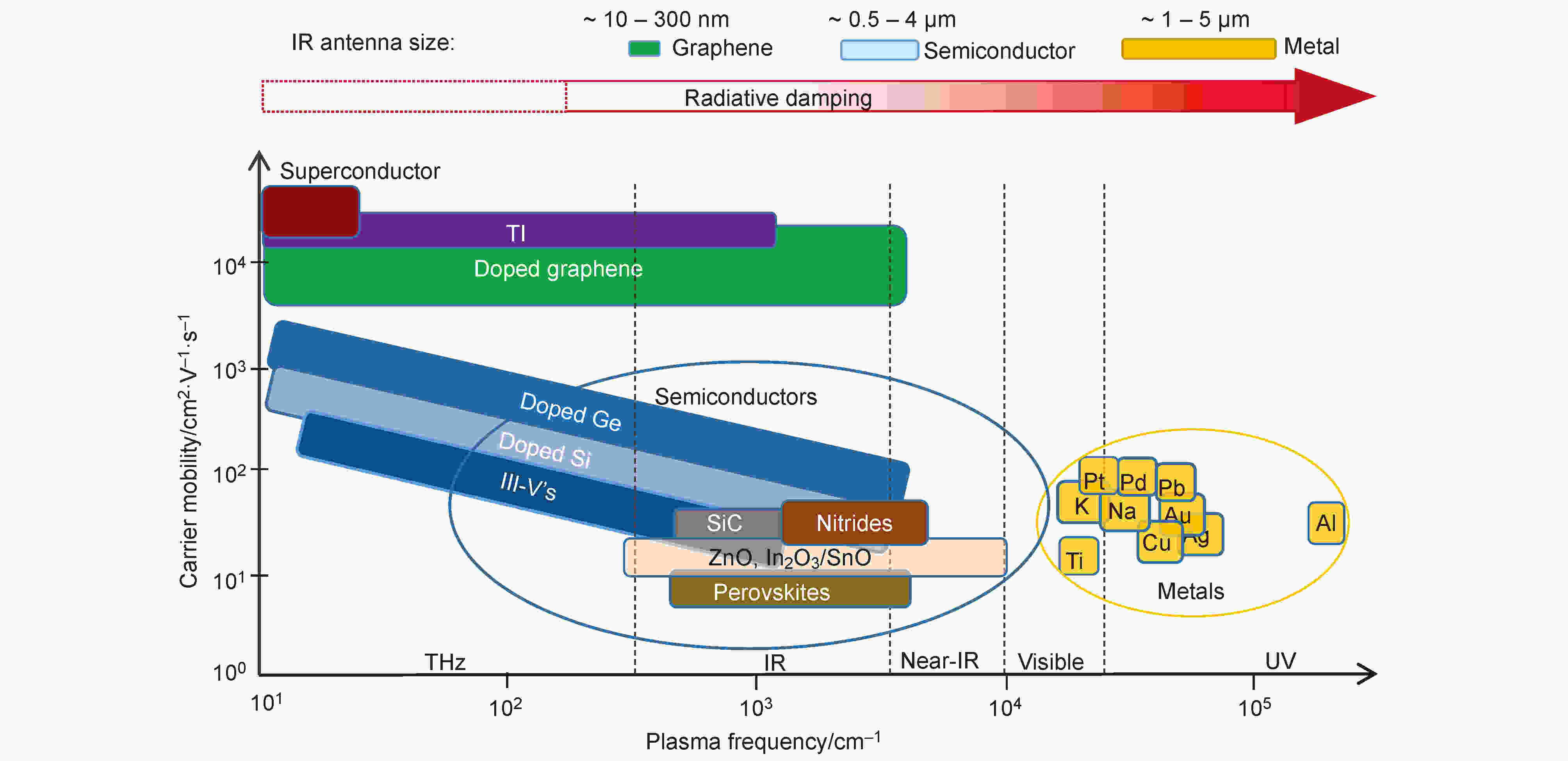
Infrared spectroscopy can accurately reflect the information of molecular vibration, and it is an important technology to characterize the composition and structure of materials. However, since the interaction between nanomaterials and infrared light is very weak due to the significant size mismatch, it is challenging to obtain the spectral information of nanomaterials in the field of infrared spectroscopy. The plasmon is a collective electron oscillation on the surface of the material inducing by the incident light, and it has excellent light field confinement, which can significantly enhance the interaction between light and nanomaterials. Graphene plasmon has prominent properties, such as high light field confinement, dynamic adjustment, and low intrinsic attenuation. Therefore it is an important solution to enhance the infrared absorption of nanomaterials. This article systematically introduces the infrared plasmon materials system. Then it summarizes the characteristics of graphene plasmon and their advantages on surface enhanced infrared spectroscopy, and it emphasizes the recent important researches and applications of graphene plasmon enhanced infrared spectroscopy in the world, including single molecular layer biochemical detection, gas identification, refractive index sensing, etc. Further prospects for the development and potential applications of graphene plasmon enhanced infrared spectroscopy are also demonstrated.
2019, 68 (14): 149101.
doi: 10.7498/aps.68.20190337
Abstract +
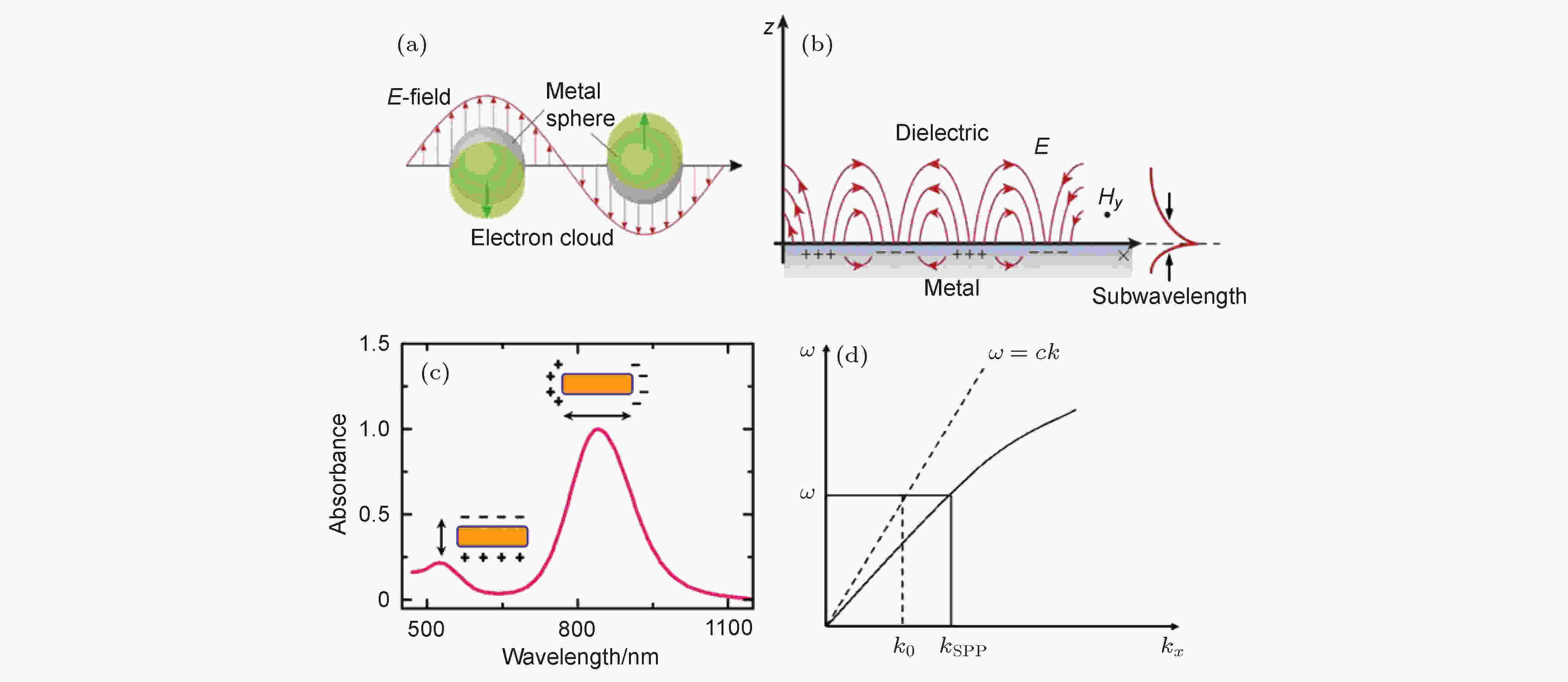
Surface plasmon polaritons (SPPs) have been widely investigated in the past decades. Due to their unique feature of field localization, optical energy can be strongly confined in the subwavelength and even nanoscale space. This strong confinement gives rise to dramatically increased electromagnetic field strength, leading to greatly enhanced light-matter interactions. The properties of SPP are strongly dependent on material, morphology and structure. The wavelength of surface plasmon resonance can be readily manipulated over broadband optical spectra, covering ultraviolet, visible, near infrared to far infrared. In this review article, both working principle and applications of surface plasmon enhanced light-matter interactions, such as fluorescence, Raman scattering, nonlinear optics, heat effects, photoacoustic effects, photo-catalysis, and photovoltaic conversion, are comprehensively reviewed. Besides, the current problems and future research directions of surface plasmons are discussed. Our paper provides valuable reference for future high-performance plasmonic device and technology applications.
GENERAL
2019, 68 (14): 140201.
doi: 10.7498/aps.68.20190333
Abstract +
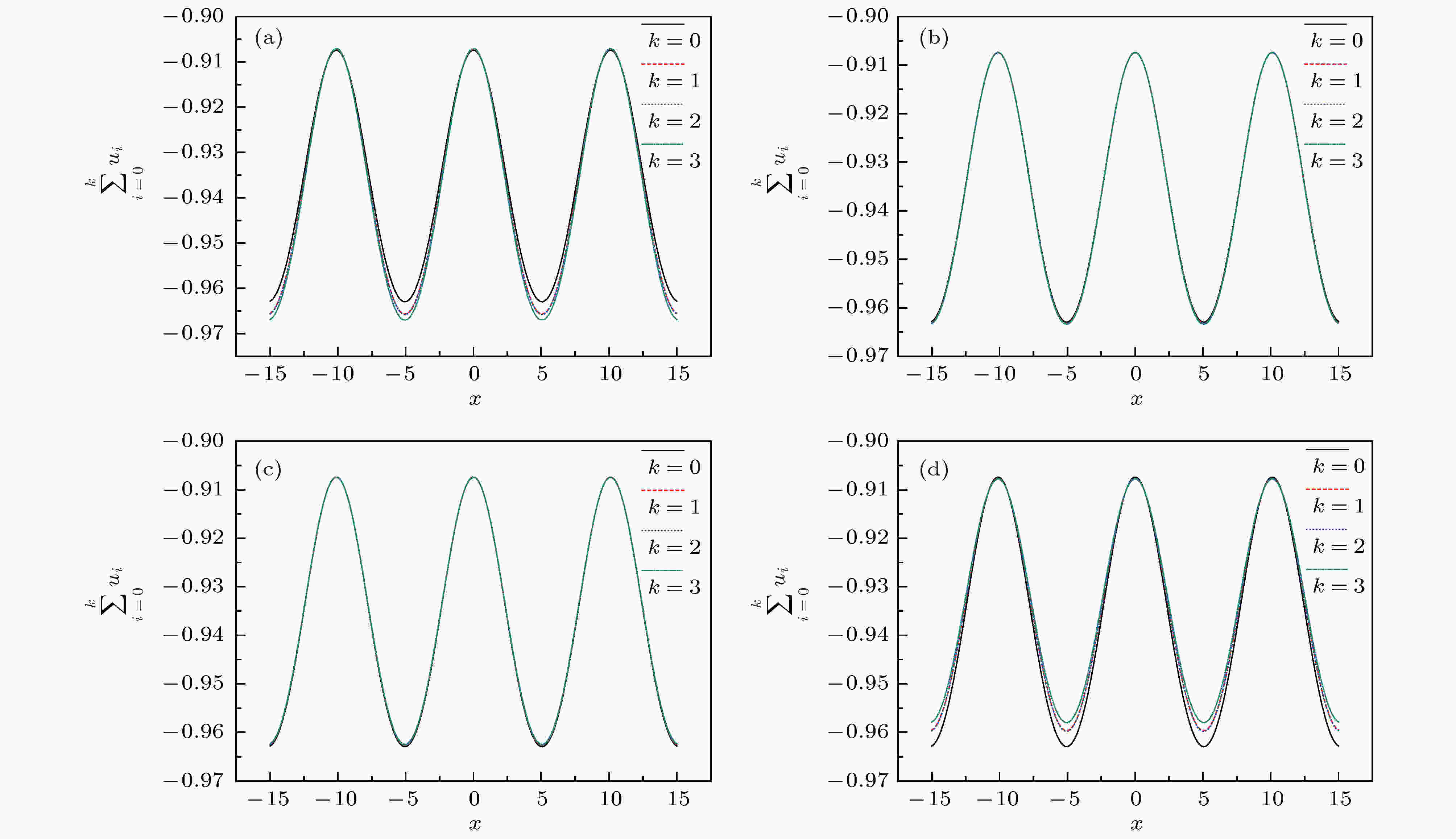
This paper is devoted to constructing series solutions to one kind of perturbed Kadomtsev-Petviashvili (KP) equations, of which the perturbation terms are of all six-order derivatives of space variable $x$ and $y$ . First, by making the series solutions expansion with respect to the homotopy parameter $q$ , the homotopy model of the perturbed KP equations can be decomposed into infinite number of approximate equations of the general form. Second, Lie symmetry method is applied to these approximate equations to achieve similarity solutions and the related similarity equations with common formulae in three cases. Third, for the first few similarity equations in the third case, Jacobi elliptic function solutions are constructed through a step-by-step procedure and are also subject to common formulae for each equation of the whole kind of perturbed KP equations. Finally, one kind of compact series solutions for the original perturbed KP equations is obtained from these Jacobi elliptic function solutions. The convergence of these series solution is dependent on perturbation parameter $\epsilon$ , auxiliary parameter $\theta$ and arbitrary constants $\{a, b, c\}$ , among which the most prominent is decreasing arbitrary constant $c$ or perturbation parameter $\varepsilon$ . For the perturbation term in perturbed KP equations, given the derivative order $n$ of $u$ with respect to $y$ , smaller (greater) $|a/b|$ causes the improved convergence provided $n\leqslant 1$ ($n\geqslant 3$ ). Nonetheless, the decrease of arbitrary constant $|c|$ or $|a/b|$ leads to the enlargement of period in a certain direction and thus should be specified appropriately. This paper also considers the perturbed KP equations with more general perturbation terms. Only if the derivative order of the perturbation term is an even number, do Jacobi elliptic function series solutions exist for perturbed KP equations. The existence of series solutions can serve as a criterion of solvability for perturbed equations.
COVER ARTICLE
2019, 68 (14): 140202.
doi: 10.7498/aps.68.20190330
Abstract +
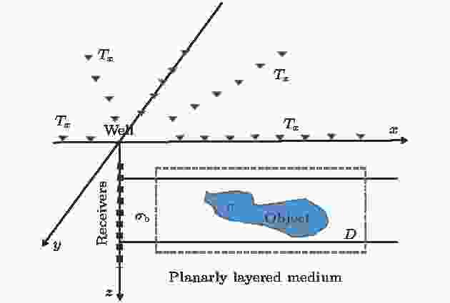
As an efficient geophysical exploration technology, well electromagnetic method is particularly applicable to oil and gas exploration in China's complex terrain areas (deserts, mountains, etc.). A serious influence of topographic relief area on the electromagnetic response of well is inevitable but challenging. To the best of our knowledge, there is no literature on modeling the electromagnetic response of three-dimensional (3D) topography with well electromagnetic method. Based on the domain decomposition, an integral equation method is presented to simulate the electromagnetic response of 3D topography in frequency domain via the well electromagnetic method. Compared with the finite difference and finite element method based on partial differential equation, this method is very efficient in simulating topographic response without huge computation or truncation boundary error accumulation or special boundary condition requirements. Firstly, an induction coefficient is defined according to the topographic relief situation. Then the computational domain consisting of the target body, background medium and 3D topography is divided into reference model, background medium and the distribution of target body medium area. According to the characteristics of each sub-region, Anderson algorithm is an analytic solution based on Gaussian filtering, which is used to provide the primary field from the excited sources in surface. And then, the stable double conjugate gradient-fast Fourier transform is incorporated into integral equation algorithm to obtain the fast 3D terrain shaft frequency domain electromagnetic responses. By comparing the calculation results using the new algorithm presented in this paper with the analytical solutions of Anderson algorithm for half-space model with surface electromagnetic method, the precision and the efficiency of this new algorithm are demonstrated. And the ability to model the electromagnetic responses of 3D topography is shown by comparing with the published results of 3D boundary integral equation. Thus, the high accuracy and high efficiency of the new algorithm presented in this paper are validated. Finally, the influence of 3D valley topography on electromagnetic field response of surface to borehole electromagnetic (SBEM) observation system is presented and analyzed. It is observed that the response of SBEM is seriously disturbed by the field of 3D valley topography which is necessarily removed. The research results presented in this paper are of significance for guiding the identification and correction of electromagnetic topographic effect from 3D SBEM.
2019, 68 (14): 140203.
doi: 10.7498/aps.68.20190340
Abstract +
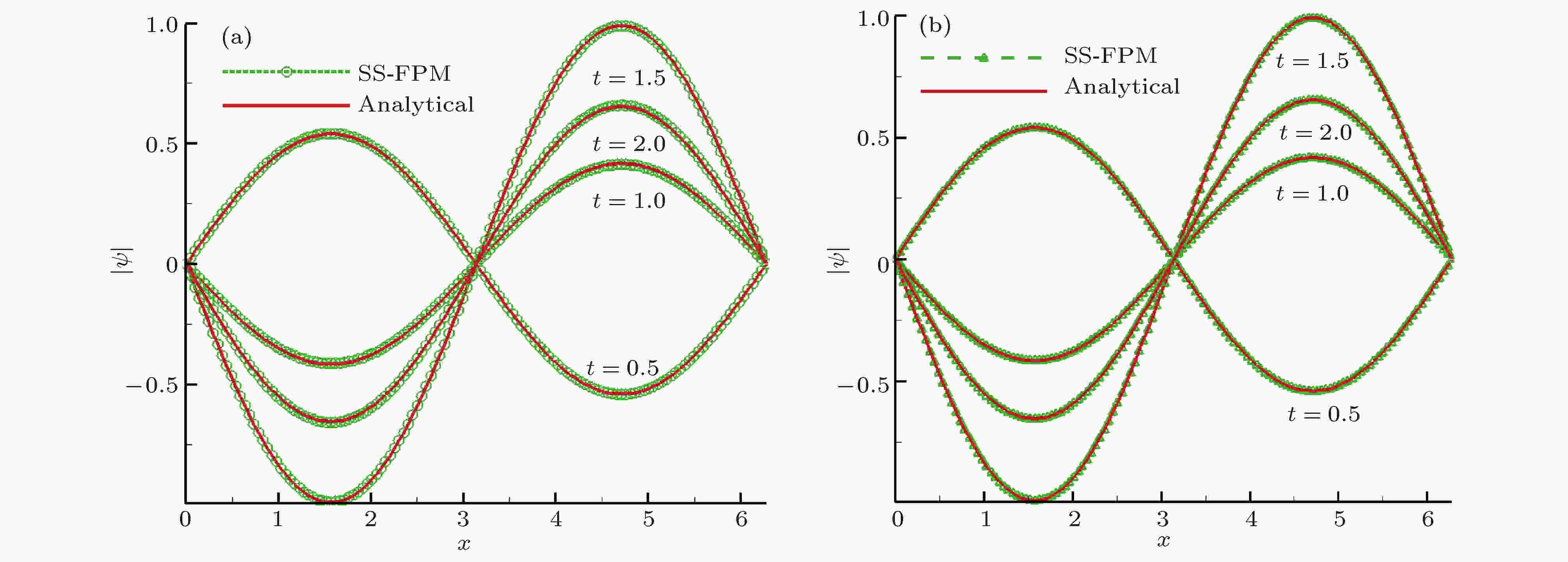
In this paper, a split-step finite pointset method (SS-FPM) is proposed and applied to the simulation of the nonlinear Schrödinger/Gross-Pitaevskii equation (NLSE/GPE) with solitary wave solution. The motivation and main idea of SS-FPMisas follows. 1) The nonlinear Schrödinger equation is first divided into the linear derivative term and the nonlinear term based on the time-splitting method. 2) The finite pointset method (FPM) based on Taylor expansion and weighted least square method is adopted, and the linear derivative term is numerically discretized with the help of Wendland weight function. Then the two-dimensional (2D) nonlinear Schrödinger equation with Dirichlet and periodic boundary conditions is simulated, and the numerical solution is compared with the analytical one. The numerical results show that the presented SS-FPM has second-order accuracy even if in the case of non-uniform particle distribution, and is easily implemented compared with the FDM, and its computational error is smaller than those in the existed corrected SPH methods. Finally, the 2D NLS equation with periodic boundary and the two-component GP equation with Dirichlet boundary and outer rotation BEC, neither of which has an analytical solution, are numerically predicted by the proposed SS-FPM. Compared with other numerical results, our numerical results show that the SS-FPM can accurately display the nonlinear solitary wave singularity phenomenon and quantized vortex process.
2019, 68 (14): 140204.
doi: 10.7498/aps.68.20190533
Abstract +
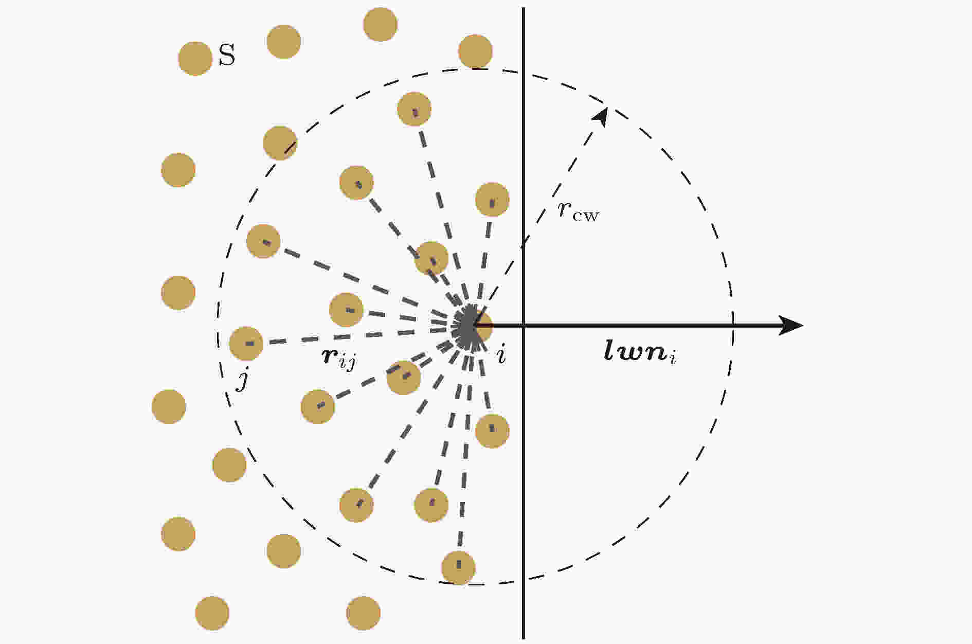
Dissipative particle dynamics (DPD) is a thriving particle-based simulation method of modeling mesoscale fluids. After two decades of evolution, DPD has shown unique advantages in researches about polymer, red blood cell, droplets wetting, etc. However, DPD is limited to relatively simple geometries due to the lack of a satisfactory boundary method. In this paper, we propose an adaptive boundary method for complex geometry, which fulfills the three basic requirements of boundary method: no penetration into the solid, no-slip near boundary, negligible fluctuation of density or temperature near boundary. Specifically, first, a new vector attribution is added to each solid particle, the attribution is named local wall normal (LWN) attribution and it is a function of its neighbor solid particle’s position, the LWN attribution is used to correct the penetrating fluid particles’ velocity and position and is computed only once if the wall is stationary. Second the surface wall particles are identified by neighbor solid fraction (φ), which indicates the percentage of surrounding space occupied by solid particles, then the wall is reconstructed by only the surface particles instead of all solid particles. By doing so, the redundant bulk particles are removed from the simulation. Third, it is detected on-the-fly whether the moving fluid particle penetrates the wall by computing its φ, the fluid particles with φ greater than 0.5 are considered to enter into the solid wall, their position and velocity will be corrected based on the local wall normal attribution. We verify that the method causes negligible density and temperature fluctuation in Poiseuille flow. Then, we illustrate the implementation of LWNM in the cases of complex blood vessel network and micro-structured surface. With this method, the obstacles in flow are no longer restricted to shapes described by functions but can be generated by CAD software, and blood vessels can also be generated by CT scan images or other experimental data. Moreover, we show a case with a bent tube and droplets inside, demonstrating the practicability of constructing complex geometry and the effectiveness of LWNM. This new boundary approach empowered DPD to simulate more realistic problems.

2019, 68 (14): 140205.
doi: 10.7498/aps.68.20190270
Abstract +
Self-assembly of nanomaterials from the drying of nanofluid films has aroused great interest due to its applications in micro/nano fabrication, ink-jet printing, and thin film coatings. Numerical models are developed to investigate the single-scale deposition structures from the drying of nanofluid films, including network structures, continuous labyrinthine, branched structures and micro-sized rings. In the case of the actual drying of nanofluid films, dual-scale cellular networks and nano-rings are also discovered. In order to study the formation mechanism of dual-scale deposition structures, a three-dimensional kinetic Monte Carlo model is developed based on two-dimensional lattice gas model, and the dynamic chemical potential which couples solvent evaporation rate is implemented. Different dynamic chemical potentials are defined for each layer of the thin-film in the model to mimic the real evaporation situation. Considering the Brownian motion and the interaction between particles, the formation of dual-scale cellular networks and nano-rings coexisting with small scale patternis achieved via coupling the chemical potential to the solvent evaporation rate. The simulation results accord well with the results from many experimentally studied de-wetting systems. The effects of the chemical potential sharpness and critical evaporation rate of fluids on the dual-scale deposition structures are discussed. It can be found that the evaporation mode of thin-film is dominated by nucleation and growth at the initial stage. If the spinodal point is passed, the residual solvent will evaporate suddenly, and the nanoparticles do not accumulate further but directly deposit into small-scale structures, thus forming a dual-scale deposition structures at the final stage of the evaporation. The simulation results also show that the chemical potential sharpness will affect the deposition structure after the mutation in a certain range. When the chemical potential sharpness equals zero, the sedimentary structure is the same as the single-scale sedimentary structure when the constant chemical potential is applied. When the chemical potential sharpness is small, the large-scale network structure interacts closely with the small-scale network structure. With the increase of chemical potential sharpness, the large-scale deposition structure remains unchanged, while the dense small-scale network structure becomes small-scale point structure. When the chemical potential sharpness exceeds a certain large value, the effect of chemical potential sharpness on the deposition structure will gradually decrease, and finally the dual-scale deposition structure will remain unchanged. The critical evaporation rate of fluids determines the area ratio of the two kind of structures in the dual-scale deposition. With the increase of the critical evaporation rate of fluids, the area ratio of small-scale structures decreases while that of the large-scale structure increases. When critical evaporation rate increases to a certain value, the final deposition structure will evolve into a single-scale deposition structure.

2019, 68 (14): 140301.
doi: 10.7498/aps.68.20190157
Abstract +
Recently, we try to answer the following question: what will happen to our life if quantum computers can be physically realized. In this research, we explore the impact of quantum algorithms on the time complexity of quantum state tomography based on the linear regression algorithm if quantum states can be efficiently prepared by classical information and quantum algorithms can be implemented on quantum computers. By studying current quantum algorithms based on quantum singular value decomposition (SVE) of calculating matrix multiplication, solving linear equations and eigenvalue and eigenstate estimation and so on, we propose a novel scheme to complete the mission of quantum state tomography. We show the calculation based on our algorithm as an example at last. Although quantum state preparations and extra measurements are indispensable in our quantum algorithm scheme compared with the existing classical algorithm, the time complexity of quantum state tomography can be remarkably declined. For a quantum system with dimension d, the entire quantum scheme can reduce the time complexity of quantum state tomography from $ O(d^{4}) $ to $ O(d\mathrm{poly}\log d) $ when both the condition number $ \kappa $ of related matrices and the reciprocal of precision $ \varepsilon $ are $ O(\mathrm{poly}\log d) $ , and quantum states of the same order $ O(d) $ can be simultaneously prepared. This is in contrast to the observation that quantum algorithms can reduce the time complexity of quantum state tomography to $O(d^3) $ when quantum states can not be efficiently prepared. In other words, the preparing of quantum states efficiently has become a bottleneck constraining the quantum acceleration.

2019, 68 (14): 140302.
doi: 10.7498/aps.68.20190462
Abstract +
Quantum communication in free space will be disturbed by natural environment, such as fog, dust, and rain, which is a difficult problem in the construction of quantum communication system. In order to solve this problem and improve the survivability of quantum communication system, we propose an adaptive parameter adjustment strategy for free-space quantum communication based on software-defined quantum communication (SDQC). Firstly, we propose a software-defined quantum communication model based on the idea of software defined networks. The architecture of SDQC is divided into four layers: transport layer, access layer, control layer, and management layer. The SDQC system sends the link information to the preset program at a management level through the real-time monitoring of channel state by the access layer. According to the link information, the management level issues instructions to the control layer to adjust the parameters such as the initial quantum state and the existence time of single quantum state, in order to improve the quantum entanglement and fidelity. Secondly, we analyze the relationship between quantum fidelity and parameters in SDQC system under three noise channels, i.e. depolarization channel, spontaneous amplitude decay channel, and phase damping channel. In the depolarized channel, the quantum fidelity F decreases with the increase of the error probability Pd of the qubit. When the error probability of qubit is certain, the system has the maximum quantum fidelity with the value of parameter x is 0.5. In the spontaneous amplitude decay channel, the quantum fidelity F decreases with the increase of the quantum state transition probability pt. When the transition probability of quantum state is certain, the higher the value of parameter x, the higher the fidelity will be. In the phase-damped channel, the quantum fidelity F decreases with the increase of the probability pc with which the qubit and the background interference equivalent quantum state have complete elastic scattering. When the probability is certain, the larger the value of |1/2 – x|, the higher the quantum fidelity of the system will be. Finally, we study the optimal values of SDQC system parameters under different environmental disturbances. The simulation results show that the optimal parameters of SDQC system are different when the parameters of three noise channels, namely depolarization, spontaneous amplitude decay and phase damping, are different. The system adaptively selects the initial quantum state and the existence time of single quantum state according to the environmental change and business demand, so that the quantum fidelity is always at the peak in the communication process. This strategy effectively improves the adaptability and comprehensive immunity of the quantum communication system.
2019, 68 (14): 140401.
doi: 10.7498/aps.68.20182301
Abstract +
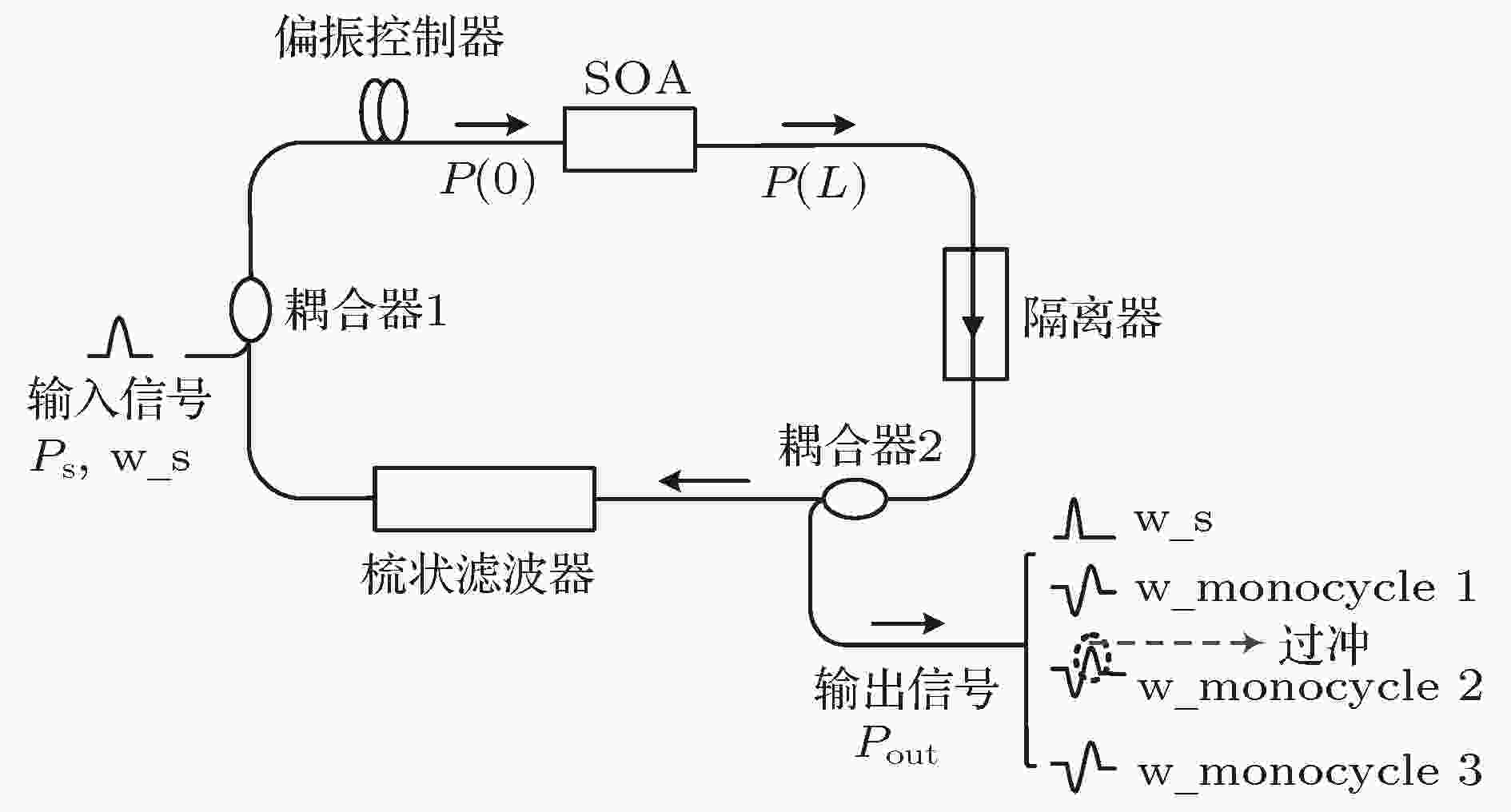
A novel scheme for all-optical ultra-wideband signal source based on semiconductor fiber ring laser (SFRL) is proposed, in which three monocycle signals can be generated simultaneously. The effect of the bias current of the semiconductor optical amplifier (SOA) in the SFRL, the wavelength of the lasing light, the power and the wavelength of input signal light on the performance of the monocycle signals are analyzed through numerical simulation. The results show that the output monocycle pulses with better symmetry can be obtained when the bias current of SOA is in a range of 200−220 mA. The average power, the amplitude of the positive and negative pulses of the output monocycle pulses increase as the wavelength of the lasing light increases. A better performance of the monocycle pulses can be obtained under lower input signal optical power. The wavelength of the input signal light has a little effect on the output monocycle pulses.
ELECTROMAGNETISM, OPTICS, ACOUSTICS, HEAT TRANSFER, CLASSICAL MECHANICS, AND FLUID DYNAMICS

2019, 68 (14): 144301.
doi: 10.7498/aps.68.20190311
Abstract +
The suppression and absorption of low-frequency noise for a fluid-filled pipe system has become a challenging task. Inspired by the properties of acoustic metamaterials, we construct a fluid-filled periodic pipe system, consisting of small-size short acoustic pipes mounted on a fluid-filled main pipe system equidistantly along the axial direction of main pipe. The short acoustic pipe is filled with fluid and gas, and the fluid section is connected to the main pipe that is filled with the same liquid. In such a periodic pipe system, an ultra-low frequency and ultra-broad band gap of acoustic waves can be generated, making the acoustic waves transmitting in the pipe system effectively attenuated within the band gap frequency range. Since the attenuation effects of the band gap on the low-frequency sound are so strong (the acoustic waves almost cannot be transmitted through the pipe system) that the periodic pipe system is referred to as a dark acoustic metamaterial (DAM)-type fluid-filled pipe system. The formation mechanism of the first band gap can be ascribed to the co-resonance of the short acoustic pipe array in the piping system, and this band gap is categorized as resonant-type BG (RBG). The contribution of short acoustic pipes is to introduce a low-frequency and large impedances spatially into the system, whereupon the transmitting waves will experience a tempestuously resonance in the pipe. As a result, the transmission of acoustic waves within the RBG is stopped. The second band gap in a higher frequency range is classified as Bragg-type band gap (BBG), since it is induced by the effects of interference between the incident, the reflected and the transmitted acoustic waves existing in the periodic units. The interference effect on the suppression of wave transmission is strengthened by the ceaselessly repeating uniform cells. The lattice constant change can bring in a modulation effects on both the BBG and the upper band edge of RBG. Increasing the volume of gas chamber in the short acoustic pipe will result in a shift of lower band edge of RBG towards the low-frequency range but has no action on the upper band edge; similarly, the augment of the liquid volume of the short acoustic pipe also lowers the band edges of RBG, however, bandwidth of the RBG will be reduced. A membrane may be used to physically separate the gas from the fluid in the short acoustic pipe, rendering the design more feasible to be realized in practical engineering. The installation of membrane will not change the low-frequency band gap properties of the DAM pipe. The obtained results show that the proposed design in this study may provide a new way to solve the defiant problem of noise control in the low frequency range for fluid piping systems.
2019, 68 (14): 144302.
doi: 10.7498/aps.68.20190408
Abstract +
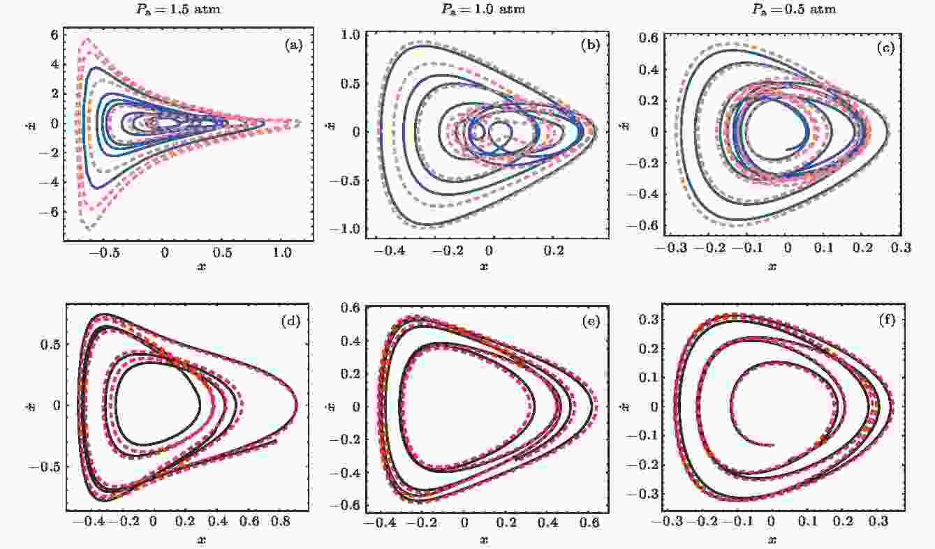
It is of great importance to investigate the dynamics of the multiple bubble system for revealing the mechanism of cavitation. Because of the secondary radiation of the oscillating bubbles, the coupled vibration of neighboring bubbles arises. Previous studies have reported that time delays appear to be more important when the coupled bubbles are close to each other. In this paper, we investigate the acoustical response of two bubble oscillators theoretically and numerically. Firstly, we modify the dynamic model equation by use of Taylor series being accurate up to terms of second order in radial displacement of bubbles. Based on the perturbation theory, the eigenmodes of the coupled-bubble system are analyzed, and two different resonant frequencies are obtained. Secondly, the effects of time delays on the coupled oscillation are analyzed numerically by use of phase diagram. When bubbles are driven by low-intensity ultrasound, we can neglect the effect of the time delay for the coupled-bubble system. Thirdly, the theoretical and numerical curve of amplitude versus frequency are compared with each other. There are two peaks on each curve on which present are two resonant regions. The relative position of the resonant peaks of the two bubbles in each region is similar for the two analytical methods. Finally, the effect of equivalent radius of bubble, equivalent radius ratio, bubble center distance, and driving pressure amplitude on the radial motion are numerically explored. With the increase of the intensity of the acoustic wave, the resonant peaks shift toward the low-frequency region. The coupled oscillation of the two bubbles of different radii could be intensified when these conditions are satisfied, such as resonant driving, equal radius, and the range of center distance smaller than 10R10. We can observe a transition phenomenon and out-of-phase fluctuation of the bubble oscillation in the strong coupling region. Therefore, bubbles play an important role of energy translator in the ultrasound applications.
CONDENSED MATTER: ELECTRONIC STRUCTURE, ELECTRICAL, MAGNETIC, AND OPTICAL PROPERTIES
2019, 68 (14): 147101.
doi: 10.7498/aps.68.20190573
Abstract +
2019, 68 (14): 147701.
doi: 10.7498/aps.68.20190222
Abstract +
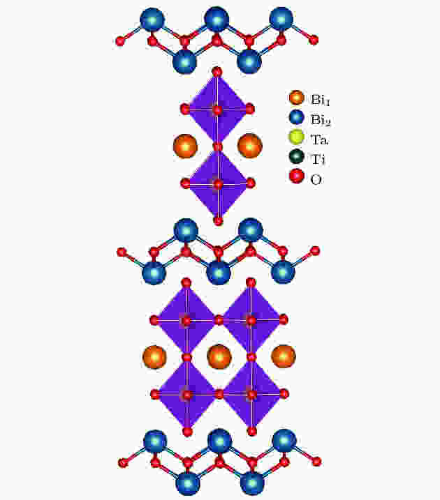
Piezoelectric materials have been extensively employed in numerous devices. With the rapid development of modern information technology, the high temperature piezoelectric materials that can work in extreme environments are in great demand. Therefore, it is urgent to investigate piezoelectric materials with high Curie temperature and strong piezoelectric performance. This paper reports the significantly improved piezoelectric properties of high temperature bismuth titanate-tantalate (Bi3TiTaO9, BTT) polycrystalline ceramics. In this work, the rare-earth cerium ions modified Bi3TiTaO9 piezoelectric ceramics are prepared by the conventional ceramic technique. The introduction of Ce ions significantly enhances the piezoelectric performance of BTT ceramics. The BTT-6Ce (BTT+0.6 wt.% CeO2) exhibits optimized piezoelectric properties with a piezoelectric coefficient d33 of 16.2 pC/N, which is four times the value of unmodified BTT (d33~4.2 pC/N). The dielectric and ferroelectric measurements indicate that Ce ions remarkably reduce the dielectric loss tanδ and increase polarizations, which are beneficial to the piezoelectric properties. The BTT and BTT-6Ce (x = 0.6) ceramics each have a high Curie temperature TC: ~890 ℃ and 879 ℃, respectively. The coercive field Ec of BTT and BTT-6Ce ceramics are 53.8 kV/cm and 57.5 kV/cm, respectively, while the remnant polarizations Pr of BTT and BTT-6Ce ceramics are 3.4 μC/cm2 and 5.4 μC/cm2, respectively, at a frequency of 1 Hz, temperature of 180 ℃, and drive field of 110 kV/cm. The thermal annealing measurements indicate that the BTT ceramics still possess stable piezoelectric properties after being annealed at 800 ℃. The results exhibit that the cerium-modified BTT ceramics are good materials for high temperature applications.
INTERDISCIPLINARY PHYSICS AND RELATED AREAS OF SCIENCE AND TECHNOLOGY
Microstructural and electrochemical properties of sulfur ion implanted nanocrystalline diamond films
2019, 68 (14): 148101.
doi: 10.7498/aps.68.20190394
Abstract +
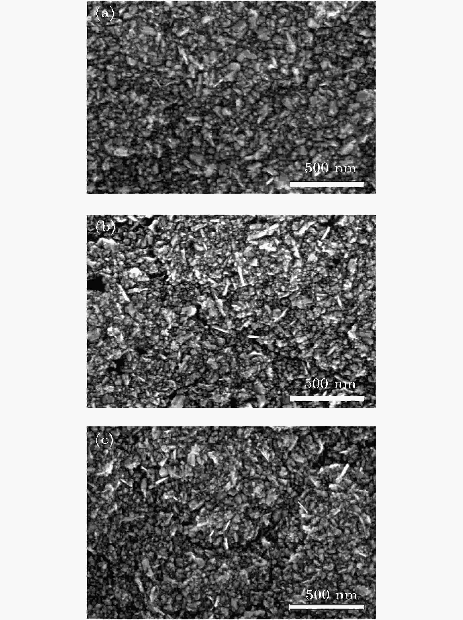
Nanocrystalline diamond (NCD) films have a composite structure composed of diamond grains and amorphous carbon grain boundaries. Compared with microcrystalline diamond (MCD) films, the NCD film grain boundaries are rich in a large number of π bonds, thus providing conductive channels. Its conductivity is 3−7 orders of magnitude higher than that of MCD, and the surface of NCD film is uniform and dense, and the roughness is lower, so the NCD film is a promising electrode material. In our previous study, microwave plasma chemical vapor deposition was successfully used to prepare n-type sulfur-doped diamond films with good electrical properties. However, the electrochemical properties of sulfur-doped nanocrystalline diamond films have not been studied till now. In the present work, the nanocrystalline diamond films are prepared by the hot-wire chemical vapor deposition. The films are subjected to ion implantation and vacuum annealing. The effects of annealing temperature on the microstructure and electrochemical properties of the films are investigated. The results show that the sulfur ion implantation is beneficial to the improvement of the electrochemical reversibility of the film. When annealed at 800 °C and below, the amorphous carbon phase at the grain boundary in the film gradually changes into the trans-acetylene phase, resulting in a gradual deterioration of electrochemical performance. When the annealing temperature rises to 900 °C, Raman spectrum and TEM results show that the film has more diamond phase content and better lattice quality, and the trans-polyacetylene in the grain boundary is cracked; XPS results indicate that the CO bond at this time, C=O bond, and π—π* content increase significantly; Hall test shows that the film mobility and carrier concentration are significantly higher than those of unannealed film. The redox peak in the electrolyte is highly symmetrical, the peak potential difference is reduced to 0.20 V, the electrochemical active area is increased to 0.64 mC/cm2, and the electrochemical reversibility is much better thanthose of samples annealed at 600 °C, 700 °C, and 800 °C, respectively.
2019, 68 (14): 148102.
doi: 10.7498/aps.68.20190252
Abstract +
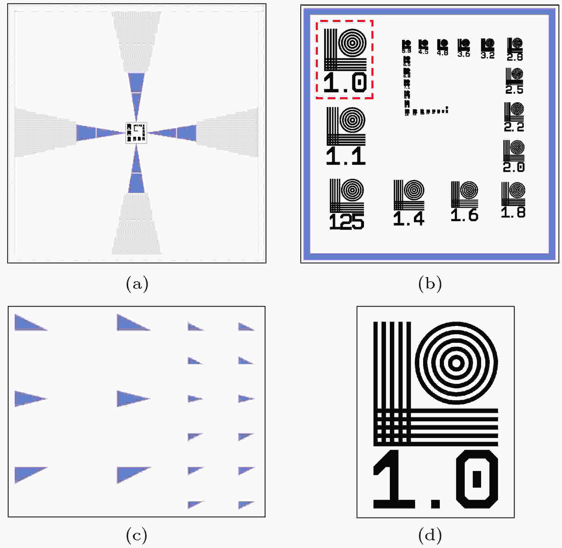
Various kinds of super-resolution optical microscope techniques have been developed to break the diffraction barrier in the past decades. Confocal laser scanning microscopy is the super-resolution microscopy. It is widely used due to high resolution and depth selectivity in obtaining images. However, there are neither accurate nor rigorous measurement methods with a nanoscale resolution. In order to measure the resolution of vector beam confocal laser scanning microscopy accurately and rigorously, a nanoscale resolution standard sample is proposed and experimentally realized. This sample is composed of a series of accurate measure patterns and a couple of arrays of triangle finding structures. It allows a wide measurement range between 40 nm to 1000 nm, and provides appropriate measurement steps and high measurement accuracy. The measurement patterns can be efficiently figured out by using the found structures, and their structure line width can be easily calculated. The first standard sample is produced on a piece of amorphous silicon by electron beam lithography and inductive coupled plasma etching technology, and measured by the scanning electron microscopy. According to the test, the sample meets the requirements of accuracy for nanoscale resolution measurement. Optical testing is applied to the sample by a vector beam confocal laser scanning microscope. And the sample shows that the resolution is 96 nm (oil immersion, refractive index 1.52) under the irradiation of 405 nm radially polarized beams, which is far beyond the diffraction barrier. Furthermore, a metal structure standard sample, which is based on a piece of indium tin oxide glass, is produced to improve the signal contrast ratio of the silicon standard sample. The measurement patterns are fabricated by electron beam lithography and electron beam evaporation and made of 10 nm titanium and 100 nm gold. It works for both reflective and transmissive confocal laser scanning microscopy, and would obtain high resolution images with a better contrast ratio. These standard samples are able to test the performance of microscope system efficiently, and provide a more rigorous way to make sub-100 nm resolution measurement and a calibration guidance for point scanning super-resolution microscope. In the meantime, we find that nanoscale opticalimaging is affected not only by sample morphology, but also by the photoelectron property of the sample. Further study is required to understand the underlying mechanism.
2019, 68 (14): 148201.
doi: 10.7498/aps.68.20190423
Abstract +
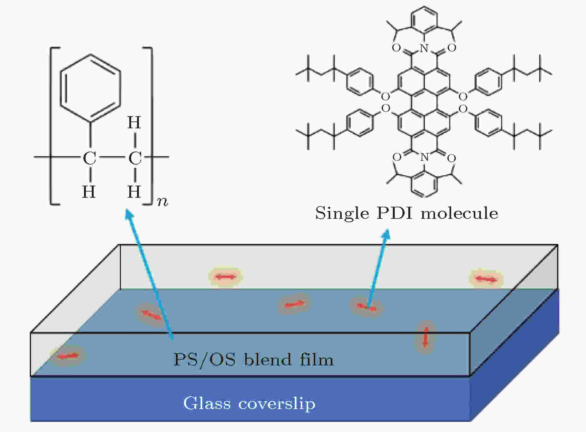
Miscible mixtures of polymer blends have physical properties that are often linked simply to the blend composition, thus offering an inexpensive and convenient method to achieve new high performance polymers. Confinement effect has been found in various polymer blend systems by the ensemble methods, but further understanding the confinement effect still requires large efforts both in experiment and in theory. Single molecule spectroscopy has the potential to provide an in-depth insight to the dynamic information by directly coupling their reorientation to the segmental relaxation of the surrounding polymer matrix. We investigate the confinement effects in polystyrene and oligostyrene blend films by using single-molecule defocused wide-field fluorescence microscopy. According to the observation for dynamic behaviors of probe molecules in the blend films of 75 wt.% and 25 wt.% polystyrene, we find that there are two types of single molecules in the blend films: rotational molecules and immobile molecules. The experimental temperature of 296 K is between the glass transition temperature (Tg) values of two pure components and also is far from the two Tg values. At the temperature, oligostyrene component is trapped by the frozen polystyrene component, but they still move locally. Therefore, the rotational and immobile molecules should couple to the oligostyrene component and polystyrene component, respectively. The distribution of rotational single molecules reveals that the confined regions randomly distribute across miscible polymer blends. The length scale of confined region is estimated to be close to that of the probe molecule by taking into account the rotational dynamics of single molecules. The local relaxation of blend film is also investigated by the rotational correlation time which can be estimated by fitting the autocorrelation curve of 〈cos(Φ)〉 with a Kohlrausch-Williams-Watts stretched exponential function. The histograms of the rotational correlation times in the blend films of 75 wt.% and 25 wt.% polystyrene are obtained respectively, which reveal the characteristic of local dynamic distribution in the confined nano-regions. We find that the dynamic behavior in the blend film of 75 wt.% polystyrene is faster than that of 25 wt.% polystyrene, indicating there is a confinement effect in the blend due to the increased constraints imposed by the polystyrene component at a higher concentration of polystyrene. All results observed in the experiment can be explained qualitatively by the self-concentration model. Our work indicates that the single molecule defocused wide-field fluorescence microscopy is a powerful tool to study the complex dynamic features in the polymer blends.

EDITOR'S SUGGESTION
2019, 68 (14): 148501.
doi: 10.7498/aps.68.20190680
Abstract +
In recent years, transition metal chalcogenides (TMDs) have attracted extensive attention of researchers due to their unique electronic structure and excellent photoelectric properties. In this paper, hexagonal structure 1T-ZrS2 quantum dots (QDs) having a monodisperse grain size of around 3.1 nm is prepared by the ultrasonic exfoliation method. The preparation includes the following steps: ZrS2 powder is ground, followed by ultrasonic exfoliation in 1-methyl-2-pyrrolidone (NMP), and 1T-ZrS2 QDs are collected after centrifugation. The structure, morphology and optical properties of the QDs are studied in detail. The structure, morphology, size distribution, and elemental composition of 1T-ZrS2 QDs are studied by using X-ray diffractometer (XRD), transmission electron microscopy (TEM), atomic force microscopy (AFM), and scanning electron microscopy (SEM). The chemical bonds of 1T-ZrS2 QDs are characterized by X-ray photoelectron microscopy (XPS) and Fourier transform infrared spectrometer (FTIR). The TEM and AFM results show that the 1T-ZrS2 QDs are spherical in shape with uniform size distribution. The sizes of the 1T-ZrS2 QDs follow a Gaussian fitted distribution with an average diameter of WC = 3.1 nm and the FWHM is 1.3 nm. The XRD diffraction pattern of 1T-ZrS2 QDs show wide dispersed diffraction peaks, which is the characteristic of QDs. The diffraction peak at 2θ = 32.3° (d = 0.278 nm) corresponds to the (101) crystal plane, and the weak diffraction peak at 2θ = 56.8°(d = 0.167 nm) belongs to the (103) crystal plane. The grain size is also calculated by using the Debye-Scherrer formula, and the calculated value (2.9 nm) is consistent with the result of TEM (3.1 nm). Two Raman vibration modes (E1g and A1g) are observed. The E1g (507.3 cm–1) and A1g (520.1 cm–1) modes relate to the in-plane and out-of-plane vibration respectively. The Raman intensity of the A1g vibration mode is stronger than that of E1g. The UV-Vis and photoluminescence (PL and PLE) characterizations exhibit that the 1T-ZrS2 QDs have two UV absorption peaks at 283 nm and 336 nm, respectively. The Stokes shift is ~130 nm, the fluorescence quantum yield reaches up to 53.3%. The results show that the 1T-ZrS2 QDs have the excellent fluorescence performance and unique optical properties, which make the 1T-ZrS2 QDs an important material for developing photodetectors, multi-color luminescent devices, and other devices.
GEOPHYSICS, ASTRONOMY, AND ASTROPHYSICS

2019, 68 (14): 149801.
doi: 10.7498/aps.68.20182071
Abstract +
Variability is one of the most important observational features of quasars, and it is still not clear that the different quasars show different characteristic variability patterns. The optical variability of quasar is very complex, and optical variability has the non-linear characteristic of complex system. In this paper, the approximate entropy method is employed to analyze the complexities of variability in the Sloan digital sky survey (SDSS) stripe 82 quasars. Firstly, in order to show that the approximate entropy method has the effective ability to distinguish the different types of time sequences, the approximate entropy of periodic sequence, noise sequence, chaotic sequence and their mixed sequences are calculated by using the analog signals. The approximate entropy method proves to be an effective method to identify different types of time sequences. Then, we present the approximate entropy of optical variability of spectroscopically-confirmed quasars from the SDSS data release 7 spectroscopic catalog, and their complexities are analyzed. The results show that the maximum approximate entropy of quasars’ optical variability is only 0.58. The complexity of quasars’ optical variability is between the complexities of periodic sequence and white noise sequence. For nearly half of the samples, the complexities of their optical variability are basically consistent with the complexity of chaotic sequence. Quasars’ optical variability is neither completely periodic nor completely stochastic.


