


-
Surface-enhanced Raman scattering (SERS) makes the Raman signals, as fingerprints of different vibration modes of chemical bonds, significant in practical applications. Two main mechanisms, chemical and physical, are attributed to the SERS of molecules adsorbed on metals. The physical mechanism plays a major role in SERS, which is the focus of our paper. Recent SERS systems are mostly based on dimer structures, i.e. nanoparticle pairs, of noble metals. Large amplification of electrical field occurs in the gap of a dimer structure compared with a single nanoparticle. The above gap positions are called as " hot spots” of SERS. In addition, the reproducibility and reliability of SERS substrates are also important for practical applications. Here we use periodical subwavelength metallic structures to meet such needs, and develop other kinds of electrical field enhancement mechanisms. We present the electrical field enhancement of the band-edge mode of surface plasmon polariton, gap plasmon polariton mode, as well as their coupling mode. We choose one-dimensional subwavelength metallic structures to clarify the physical mechanism. Our purpose is to develop subwavelength metallic structures with even and intensive " hot spots”, serving as ultrasensitive solid-state SERS substrates with excellent reproducibility and reliability.
-
Keywords:
- surface-enhanced Raman scattering /
- surface plasmon polaritons /
- subwavelength structures /
- near-field optics
[1] Fleischmann M, Hendra P J, McQuillan A J 1974 Chem. Phys. Lett. 26 163
 Google Scholar
[2] Ringler M, Klar T A, Schwemer A, Susha A S, Stehr J, Raschke G, Funk S, Borowski M, Nichtl A, Kuerzinger K, Phillips R T, Feldmann J 2007 Nano Lett. 7 2753
Google Scholar
[3] Huang J S, Callegari V, Geisler P, Bruning C, Kern J, Prangsma J C, Wu X, Feichtner T, Ziegler J, Weinmann P, Kamp M, Forchel A, Biagioni P, Sennhauser U, Hecht B 2010 Nat. Commun. 1 150
[4] Benz F, Tserkezis C, Herrmann L O, de Nijs B, Sanders A, Sigle D O, Pukenas L, Evans S D, Aizpurua J, Baumberg J J 2015 Nano Lett. 15 669
Google Scholar
[5] Nie S M, Emory S R 1997 Science 275 1102
Google Scholar
[6] Kleinman S L, Ringe E, Valley N, Wustholz K L, Phillips E, Scheidt K A, Schatz G C, van Duyne R P 2011 J. Am. Chem. Soc. 133 4115
Google Scholar
[7] Kneipp J, Kneipp H, Kneipp K 2008 Chem. Soc. Rev. 37 1052
Google Scholar
[8] Qian X M, Nie S M 2008 Chem. Soc. Rev. 37 912
Google Scholar
[9] Duan H G, Hu H L, Kumar K, Shen Z X, Yang J K W 2011 ACS Nano 5 7593
Google Scholar
[10] Feng L, Ma R, Wang Y, Xu D, Xiao D, Liu L, Lu N 2015 Nano Res. 8 3715
Google Scholar
[11] Im H, Bantz K C, Lindquist N C, Haynes C L, Oh S H 2010 Nano Lett. 10 2231
Google Scholar
[12] Li J F, Huang Y F, Ding Y, Yang Z L, Li S B, Zhou X S, Fan F R, Zhang W, Zhou Z Y, Wu D Y, Ren B, Wang Z L, Tian Z Q 2010 Nature 464 392
Google Scholar
[13] Wang H H, Liu C Y, Wu S B, Liu N W, Peng C Y, Chan T H, Hsu C F, Wang J K, Wang Y L 2006 Adv. Mater. 18 491
Google Scholar
[14] Engheta N, Ziolkowski R W 2006 Metamaterials: Physics and Engineering Explorations (Hoboken: Wiley)
[15] Yu N F, Genevet P, Kats M A, Aieta F, Tetienne J P, Capasso F, Gaburro Z 2011 Science 334 333
Google Scholar
[16] Le Ru E C, Etchegoin P G 2006 Chem. Phys. Lett. 423 63
Google Scholar
[17] Sakoda K 1999 Opt. Express 4 167
Google Scholar
[18] Ding F, Yang Y Q, Deshpande R A, Bozhevolnyi S I 2018 Nanophotonics 7 1129
Google Scholar
[19] Le Ru E C, Blackie E, Meyer M, Etchegoin P G 2007 J. Phys. Chem. C 111 13794
-
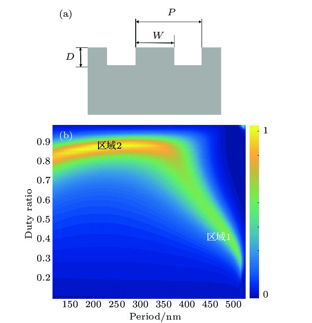
图 1 (a)一维金属亚波长结构示意图; (b) D = 30 nm时, SERS增强因子随周期P和占空比γ的变化
Figure 1. (a) The cross-sectional sketch of the one-dimensional gratings; (b) the calculated enhancement factor as a function of the period and duty ratio.
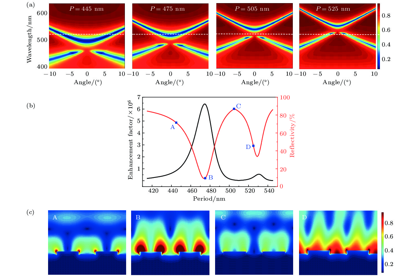
图 2 (a)计算的不同周期的SPP能带结构图, 其中白色虚线表示λ = 532 nm位置; (b)计算的不同周期结构在532 nm的反射率以及SERS增强因子; (c)对应(b)中四个不同周期值的电场分布图
Figure 2. (a) The calculated bandgap structures for various periods but the same depth and duty ratio; (b) the calculated enhancement factor and reflectivity as a function of the period; (c) the calculated electric field distribution of structures with different periods corresponding to the positions A, B, C, and D in (b).
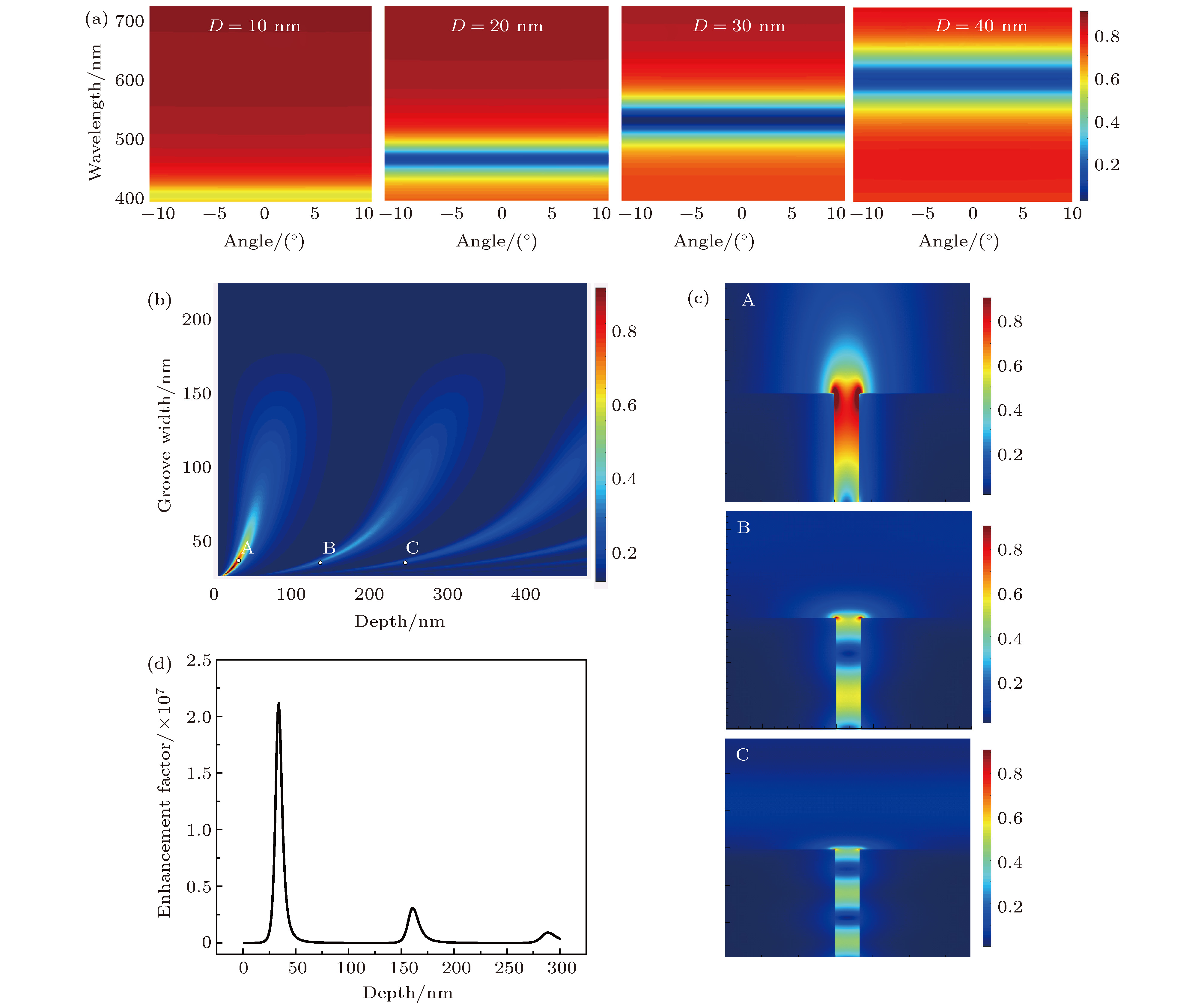
图 3 (a)计算的不同深度的GPP能带结构图; (b)周期P = 200 nm时, 计算的SERS增强因子随深度以及槽的宽度的变化图; (c)图(b)中三个位置处的电场分布图; (d)周期P = 200 nm, 槽的宽度Wg = 20 nm时, 计算的不同深度的SERS增强因子
Figure 3. (a) The calculated bandgap structures for different depths but the same period and width; (b) the calculated enhancement factor as a function of depth and groove width, in which the period is set as 200 nm; (c) the electric field distribution of structures with different depths and widths, corresponding to the positions A, B, and C in (b); (d) the calculated enhancement factor as a function of the depth.
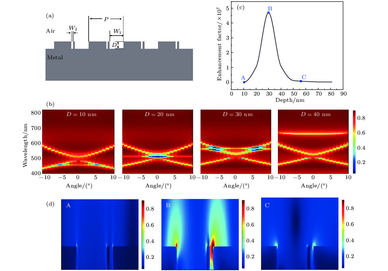
图 4 (a)双槽结构示意图; (b)计算的不同深度的双槽结构的能带结构图; (c)计算的不同深度的SERS增强因子; (d)计算的不同深度下的电场分布图, 对应于(c)中的A, B和C点的参数
Figure 4. (a) The cross-sectional sketch of the structure with double grooves; (b) the calculated bandgap structures for different depths with P = 475 nm, W1 = 182 nm and W2 = 20 nm; (c) the calculated enhancement factor as a function of the depth; (d) the calculated electric field distribution of different depth corresponding to the positions A, B, and C in (c).
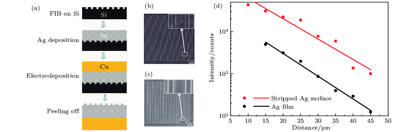
图 5 (a)撕膜的工艺流程; (b)镀Ag膜样品表面直接加工光栅的SEM图; (c)通过撕膜方法获得光栅的SEM图; (d)镀膜和撕膜Ag表面的SPP传播测量结果
Figure 5. (a) Schematic diagram of the template stripping process; (b) the SEM images of gratings on coated Ag film; (c) the SEM images of stripped Ag gratings; (d) the propagation measurements of 633 nm laser on conventional Ag film and stripped Ag surface.
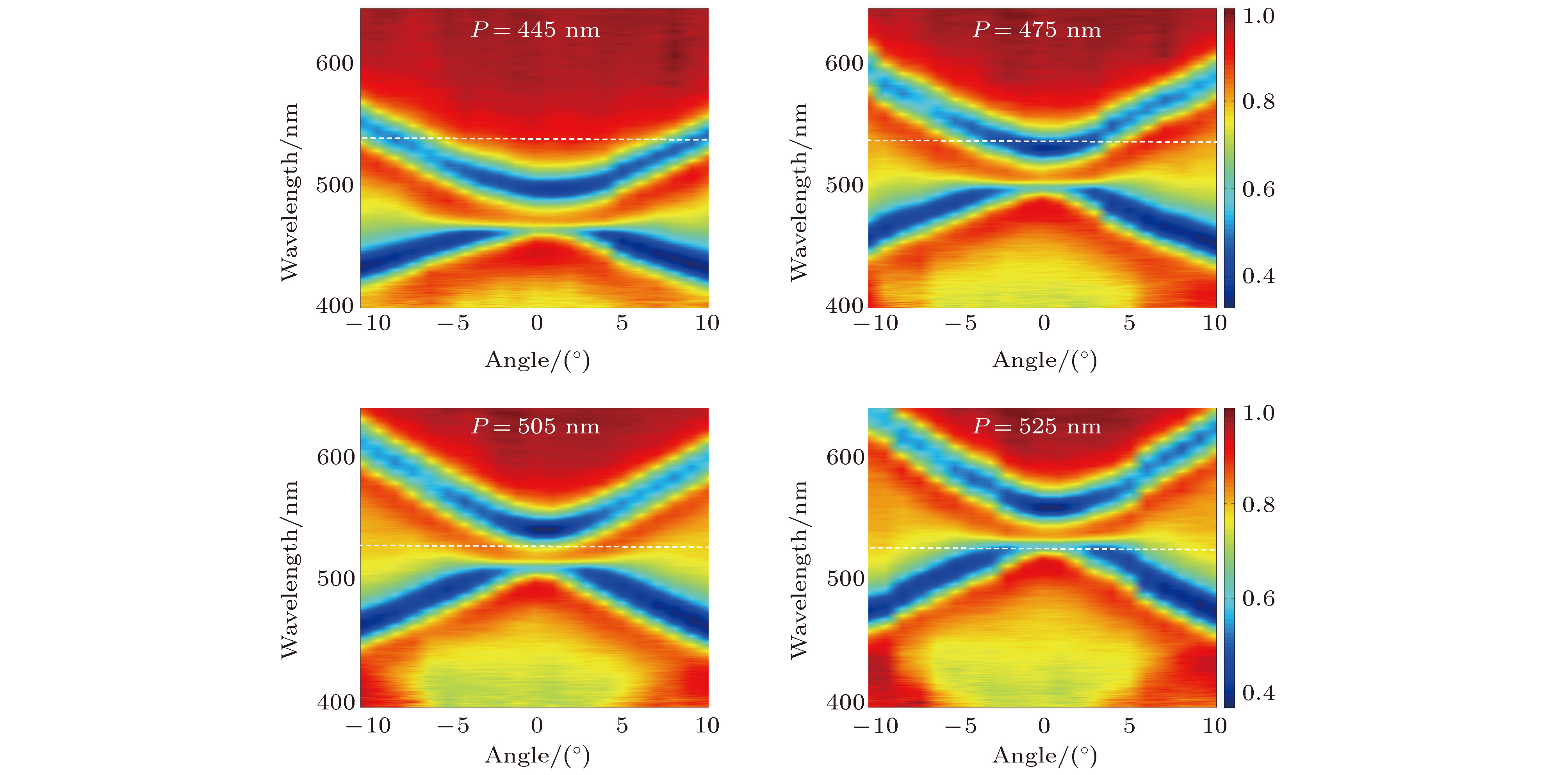
图 6 不同周期的SPP能带结构测量结果, 与图2(a)中的计算结果相对应
Figure 6. Experimental bandgap structures corresponding to those in Fig. 2 (a).
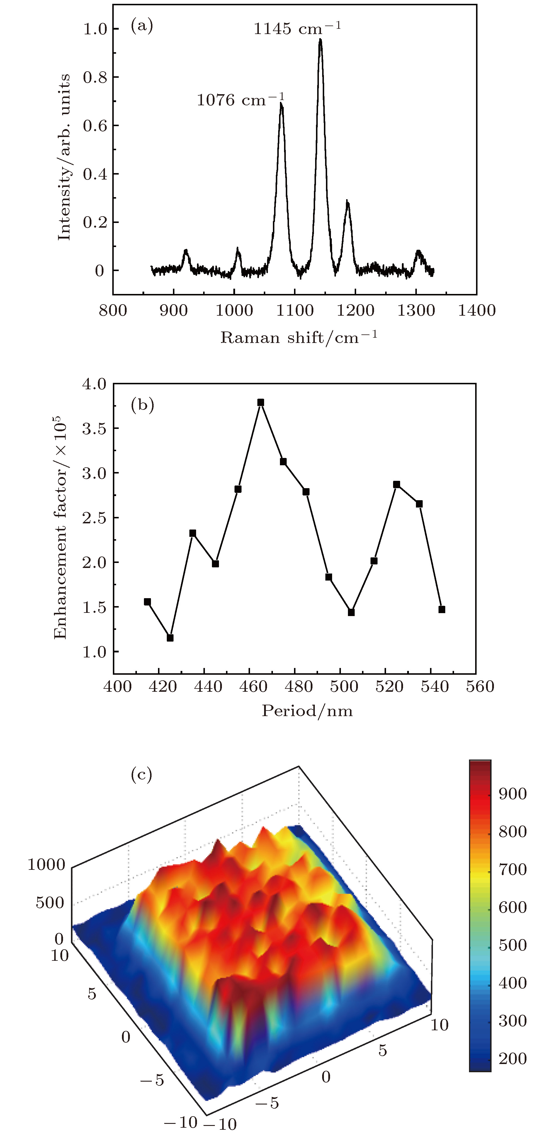
图 7 (a) 4-ATP分子在Ag基板上的拉曼散射光谱; (b)测量的不同周期结构的SERS增强因子; (c)拉曼散射的空间扫描测量结果图
Figure 7. (a) The Raman spectrum of 4-ATP molecules on Ag substrate; (b) the experimental enhancement factor as a function of the period; (c) SERS mapping image at 1145 cm–1
-
[1] Fleischmann M, Hendra P J, McQuillan A J 1974 Chem. Phys. Lett. 26 163
Google Scholar
[2] Ringler M, Klar T A, Schwemer A, Susha A S, Stehr J, Raschke G, Funk S, Borowski M, Nichtl A, Kuerzinger K, Phillips R T, Feldmann J 2007 Nano Lett. 7 2753
Google Scholar
[3] Huang J S, Callegari V, Geisler P, Bruning C, Kern J, Prangsma J C, Wu X, Feichtner T, Ziegler J, Weinmann P, Kamp M, Forchel A, Biagioni P, Sennhauser U, Hecht B 2010 Nat. Commun. 1 150
[4] Benz F, Tserkezis C, Herrmann L O, de Nijs B, Sanders A, Sigle D O, Pukenas L, Evans S D, Aizpurua J, Baumberg J J 2015 Nano Lett. 15 669
Google Scholar
[5] Nie S M, Emory S R 1997 Science 275 1102
Google Scholar
[6] Kleinman S L, Ringe E, Valley N, Wustholz K L, Phillips E, Scheidt K A, Schatz G C, van Duyne R P 2011 J. Am. Chem. Soc. 133 4115
Google Scholar
[7] Kneipp J, Kneipp H, Kneipp K 2008 Chem. Soc. Rev. 37 1052
Google Scholar
[8] Qian X M, Nie S M 2008 Chem. Soc. Rev. 37 912
Google Scholar
[9] Duan H G, Hu H L, Kumar K, Shen Z X, Yang J K W 2011 ACS Nano 5 7593
Google Scholar
[10] Feng L, Ma R, Wang Y, Xu D, Xiao D, Liu L, Lu N 2015 Nano Res. 8 3715
Google Scholar
[11] Im H, Bantz K C, Lindquist N C, Haynes C L, Oh S H 2010 Nano Lett. 10 2231
Google Scholar
[12] Li J F, Huang Y F, Ding Y, Yang Z L, Li S B, Zhou X S, Fan F R, Zhang W, Zhou Z Y, Wu D Y, Ren B, Wang Z L, Tian Z Q 2010 Nature 464 392
Google Scholar
[13] Wang H H, Liu C Y, Wu S B, Liu N W, Peng C Y, Chan T H, Hsu C F, Wang J K, Wang Y L 2006 Adv. Mater. 18 491
Google Scholar
[14] Engheta N, Ziolkowski R W 2006 Metamaterials: Physics and Engineering Explorations (Hoboken: Wiley)
[15] Yu N F, Genevet P, Kats M A, Aieta F, Tetienne J P, Capasso F, Gaburro Z 2011 Science 334 333
Google Scholar
[16] Le Ru E C, Etchegoin P G 2006 Chem. Phys. Lett. 423 63
Google Scholar
[17] Sakoda K 1999 Opt. Express 4 167
Google Scholar
[18] Ding F, Yang Y Q, Deshpande R A, Bozhevolnyi S I 2018 Nanophotonics 7 1129
Google Scholar
[19] Le Ru E C, Blackie E, Meyer M, Etchegoin P G 2007 J. Phys. Chem. C 111 13794

 DownLoad:
Catalog
Metrics
- Abstract views: 15156
- PDF Downloads: 352
- Cited By: 0
