-
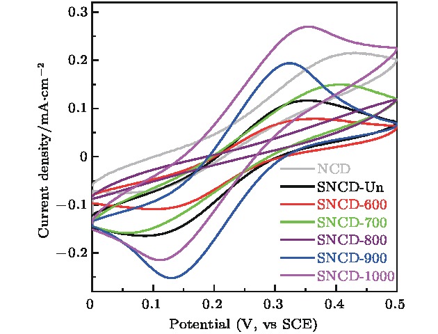
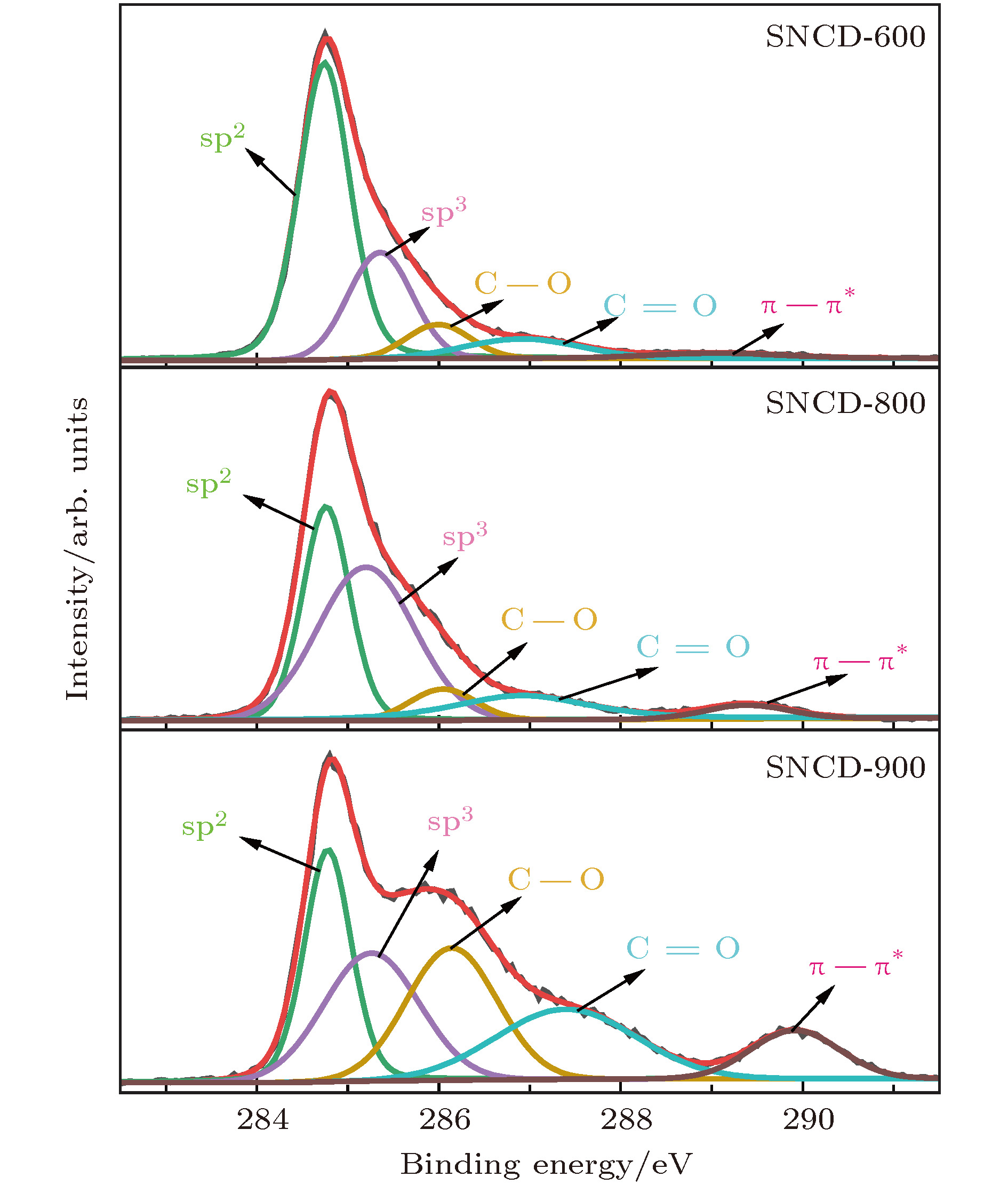
Nanocrystalline diamond (NCD) films have a composite structure composed of diamond grains and amorphous carbon grain boundaries. Compared with microcrystalline diamond (MCD) films, the NCD film grain boundaries are rich in a large number of π bonds, thus providing conductive channels. Its conductivity is 3−7 orders of magnitude higher than that of MCD, and the surface of NCD film is uniform and dense, and the roughness is lower, so the NCD film is a promising electrode material. In our previous study, microwave plasma chemical vapor deposition was successfully used to prepare n-type sulfur-doped diamond films with good electrical properties. However, the electrochemical properties of sulfur-doped nanocrystalline diamond films have not been studied till now. In the present work, the nanocrystalline diamond films are prepared by the hot-wire chemical vapor deposition. The films are subjected to ion implantation and vacuum annealing. The effects of annealing temperature on the microstructure and electrochemical properties of the films are investigated. The results show that the sulfur ion implantation is beneficial to the improvement of the electrochemical reversibility of the film. When annealed at 800 °C and below, the amorphous carbon phase at the grain boundary in the film gradually changes into the trans-acetylene phase, resulting in a gradual deterioration of electrochemical performance. When the annealing temperature rises to 900 °C, Raman spectrum and TEM results show that the film has more diamond phase content and better lattice quality, and the trans-polyacetylene in the grain boundary is cracked; XPS results indicate that the CO bond at this time, C=O bond, and π—π* content increase significantly; Hall test shows that the film mobility and carrier concentration are significantly higher than those of unannealed film. The redox peak in the electrolyte is highly symmetrical, the peak potential difference is reduced to 0.20 V, the electrochemical active area is increased to 0.64 mC/cm2, and the electrochemical reversibility is much better thanthose of samples annealed at 600 °C, 700 °C, and 800 °C, respectively.
-
Keywords:
- nanocrystalline diamond films /
- sulfur ion implantation /
- electrochemical properties /
- microstructure
[1] Chailapakul O, Aksharanandana P, Frelink T 2001 Sens. Actuators, B 80 193
 Google Scholar
[2] Denisova A E, Pleskov Y V 2008 Russ. J. Electrochem. 44 1083
 Google Scholar
[3] Green S J, Mahe L S A, Rosseinsky D R 2013 Electrochim. Acta 107 111
 Google Scholar
[4] ubomír Š L, Jozef S, Jana S 2013 Electrochim. Acta 87 503
 Google Scholar
[5] Xu H, Chen C K, Fan D, Jiang M Y, Li Xiao, Hu X J 2019 Carbon 145 187
 Google Scholar
[6] 顾珊珊, 胡晓君, 黄凯 2013 物理学报 62 118101
 Google Scholar
Gu S S, Hu X J, Huang K 2013 Acta Phys. Sin. 62 118101
 Google Scholar
[7] 潘金平, 胡晓君, 陆利平, 印迟 2010 物理学报 59 7410
 Google Scholar
Pan J P, Hu X J, Lu L P, Yin C 2010 Acta Phys. Sin. 59 7410
 Google Scholar
[8] Wang S, Swope V M, Butler J E 2009 Diamond Relat. Mater. 18 669
 Google Scholar
[9] Barek J, Jandová K, Pecková K, Zima J 2007 Talanta 74 421
 Google Scholar
[10] Williams O A, Nesladek M, Daenen M, Michaelson S, Hoffman A, Osawa E, Heaner K, Jackman R B 2008 Diamond Relat. Mater. 17 1080
 Google Scholar
[11] Jiang M Y, Yu H, Li X, Lu S H, Hu X J 2017 Electrochim. Acta 258 61
 Google Scholar
[12] Hu X J, Ye J S, Hu H, Chen X H, Shen Y G 2011 Appl. Phys. Lett. 99 131902
 Google Scholar
[13] Hu X J, Ye J S, Liu H J, Shen Y G, Chen X H 2011 J. Appl. Phys. 109 053524
 Google Scholar
[14] 王锐, 胡晓君 2014 物理学报 63 148102
 Google Scholar
Wang R, Hu X J 2014 Acta Phys. Sin. 63 148102
 Google Scholar
[15] 胡晓君, 李荣斌, 沈荷生, 戴永兵, 何贤昶 2004 半导体学报 25 8
Hu X J, Li R B, Shen H S, Dai Y B, He X C 2004 Journal Semiconductors 25 8
[16] Galář P, Dzurňák B, Varga M 2014 Opt. Mater. Express 4 624
 Google Scholar
[17] Ferrari A C, Robertson 2001 Phys. Rev. B 64 075414
 Google Scholar
[18] Ferrari A C, Robertson 2001 Phys. Rev. B 63 121405
 Google Scholar
[19] Chhowalla M, Ferrari A C, Robertson J, Amaratunga G A J 2000 Appl. Phys. Lett. 76 1419
 Google Scholar
[20] Ferrari A C, Robertson J 2004 P. Roy. Soc. A-Math. Phy. 362 2477
[21] Mei Y S, Fan D, Lu S H, Shen Y G, Hu X J 2016 J. Appl. Phys. 120 225107
 Google Scholar
[22] Hu X J, Chen C K, Lu S H 2016 Carbon 98 671
 Google Scholar
[23] Pleskov Y V, Krotova M D, Ralchenko V G 2010 Russ. J. Electrochem. 46 1063
 Google Scholar
[24] Pleskov Y V, Krotova M D, Saveliev A V, Ralchenko V G 2007 Diamond Relat. Mater. 16 2114
 Google Scholar
[25] Simon N, Girard H, Ballutaud D 2005 Diamond Relat. Mater. 14 1179
 Google Scholar
[26] Osswald S, Yushin G, Mochalin V, Kucheyev S O, Gogotsi Y 2006 J. Am. Chem. Soc. 128 11635
 Google Scholar
-
图 4 不同退火温度的SNCD薄膜的(a)可见光Raman图谱及其Gaussian拟合结果; (b)拟合得到的金刚石与TPA含量演化图; (c) 拟合得到的ID/IG值演化图; (d)拟合得到的金刚石峰半峰宽演化图
Figure 4. (a) The visible Raman map and its Gaussian fitting results and the evolution of, (b) ID/ IG value and the G peak positon, (c) the diamond and TPA content and (d) the peak width of the diamond peak (FWHMDia) of SNCD film with different annealing temperatures.
图 5 (a) SNCD-Un, (b) SNCD-600, (c) SNCD-800, (d) SNCD-900的HRTEM图(每张图片的右上角FT0代表该区域的整个傅里叶变换图, FT1, FT2, FT3分别表示对图上所标该区域做傅里叶变换)
Figure 5. HRTEM image of (a) SNCD-Un, (b) SNCD-600, (c) SNCD-800, (d) SNCD-900 (the upper right corner of each picture, FT0, represents the entire Fourier transform of the region; FT1, FT2, and FT3 respectively represent the Fourier transform of the region marked on the graph).
表 1 不同退火温度的SNCD电极在100 mV/s扫描速率下峰电位信息及电化学活性面积
Table 1. Peak potential information and electrochemically active area of SNCD electrodes with different annealing temperatures at a scanning rate of 100 mV/s.
样品名称 峰电位差ΔEp/V 电化学活性
面积ΔQC/mC·cm–2NCD 0.38 0.31 SNCD-Un 0.26 0.39 SNCD-600 0.27 0.36 SNCD-700 0.35 0.32 SNCD-800 — 0.11 SNCD-900 0.20 0.64 SNCD-1000 0.23 0.69 表 2 SNCD-Un和SNCD-900的霍尔效应测试结果
Table 2. Hall effects test results of samples SNCD-Un and SNCD-900.
样品名称 电阻率/Ω·square–1 霍尔系数/m2·C–1 迁移率/cm2·V–1·s–1 载流子浓度/cm–2 导电类型 SNCD-Un 0.319 2.26 14.2 2.76 × 10¹⁴ n SNCD-900 0.365 10.30 56.2 6.08 × 10¹⁴ n 表 3 由C 1s谱图拟合得到的SNCD-600, SNCD-800和SNCD-900表面各键的含量
Table 3. Contents of the bonds on the surface of SNCD-600, SNCD-800 and SNCD-900 calculated by C 1s spectral fitting.
样品名称 sp2C/% sp3C/% C—O/% C=O/% π—π*/% SNCD-600 56.53 25.78 7.55 7.80 2.33 SNCD-800 49.09 28.73 8.35 8.88 4.92 SNCD-900 20.37 30.47 20.97 19.62 8.58 -
[1] Chailapakul O, Aksharanandana P, Frelink T 2001 Sens. Actuators, B 80 193
 Google Scholar
[2] Denisova A E, Pleskov Y V 2008 Russ. J. Electrochem. 44 1083
 Google Scholar
[3] Green S J, Mahe L S A, Rosseinsky D R 2013 Electrochim. Acta 107 111
 Google Scholar
[4] ubomír Š L, Jozef S, Jana S 2013 Electrochim. Acta 87 503
 Google Scholar
[5] Xu H, Chen C K, Fan D, Jiang M Y, Li Xiao, Hu X J 2019 Carbon 145 187
 Google Scholar
[6] 顾珊珊, 胡晓君, 黄凯 2013 物理学报 62 118101
 Google Scholar
Gu S S, Hu X J, Huang K 2013 Acta Phys. Sin. 62 118101
 Google Scholar
[7] 潘金平, 胡晓君, 陆利平, 印迟 2010 物理学报 59 7410
 Google Scholar
Pan J P, Hu X J, Lu L P, Yin C 2010 Acta Phys. Sin. 59 7410
 Google Scholar
[8] Wang S, Swope V M, Butler J E 2009 Diamond Relat. Mater. 18 669
 Google Scholar
[9] Barek J, Jandová K, Pecková K, Zima J 2007 Talanta 74 421
 Google Scholar
[10] Williams O A, Nesladek M, Daenen M, Michaelson S, Hoffman A, Osawa E, Heaner K, Jackman R B 2008 Diamond Relat. Mater. 17 1080
 Google Scholar
[11] Jiang M Y, Yu H, Li X, Lu S H, Hu X J 2017 Electrochim. Acta 258 61
 Google Scholar
[12] Hu X J, Ye J S, Hu H, Chen X H, Shen Y G 2011 Appl. Phys. Lett. 99 131902
 Google Scholar
[13] Hu X J, Ye J S, Liu H J, Shen Y G, Chen X H 2011 J. Appl. Phys. 109 053524
 Google Scholar
[14] 王锐, 胡晓君 2014 物理学报 63 148102
 Google Scholar
Wang R, Hu X J 2014 Acta Phys. Sin. 63 148102
 Google Scholar
[15] 胡晓君, 李荣斌, 沈荷生, 戴永兵, 何贤昶 2004 半导体学报 25 8
Hu X J, Li R B, Shen H S, Dai Y B, He X C 2004 Journal Semiconductors 25 8
[16] Galář P, Dzurňák B, Varga M 2014 Opt. Mater. Express 4 624
 Google Scholar
[17] Ferrari A C, Robertson 2001 Phys. Rev. B 64 075414
 Google Scholar
[18] Ferrari A C, Robertson 2001 Phys. Rev. B 63 121405
 Google Scholar
[19] Chhowalla M, Ferrari A C, Robertson J, Amaratunga G A J 2000 Appl. Phys. Lett. 76 1419
 Google Scholar
[20] Ferrari A C, Robertson J 2004 P. Roy. Soc. A-Math. Phy. 362 2477
[21] Mei Y S, Fan D, Lu S H, Shen Y G, Hu X J 2016 J. Appl. Phys. 120 225107
 Google Scholar
[22] Hu X J, Chen C K, Lu S H 2016 Carbon 98 671
 Google Scholar
[23] Pleskov Y V, Krotova M D, Ralchenko V G 2010 Russ. J. Electrochem. 46 1063
 Google Scholar
[24] Pleskov Y V, Krotova M D, Saveliev A V, Ralchenko V G 2007 Diamond Relat. Mater. 16 2114
 Google Scholar
[25] Simon N, Girard H, Ballutaud D 2005 Diamond Relat. Mater. 14 1179
 Google Scholar
[26] Osswald S, Yushin G, Mochalin V, Kucheyev S O, Gogotsi Y 2006 J. Am. Chem. Soc. 128 11635
 Google Scholar
Catalog
Metrics
- Abstract views: 11895
- PDF Downloads: 76
- Cited By: 0


 DownLoad:


