


-
原子尺度表面吸附Au原子的物理化学性质对研究纳米器件的制备以及表面催化等起着非常重要的作用. 利用调频开尔文探针力显微镜研究了室温下Au在Si(111)-(7×7)表面吸附的电荷分布的特性. 首先, 利用自制超高真空开尔文探针力显微镜成功得到了原子尺度Au在Si(111)-(7×7) 不同吸附位的表面形貌与局域接触电势差(LCPD); 其次, 通过原子间力谱与电势差分析了Au/Si(111)-(7×7) 特定原子位置的原子特性, 实现了原子识别; 并通过结合差分电荷密度计算解释了Au/Si(111)-(7×7)表面间电荷转移与Au的吸附特性. 结果显示, Au原子吸附有单原子和团簇形式. 其中, Au团簇以6个原子为一组呈六边形结构吸附于Si(111)-(7×7) 的层错半单胞内的3个中心原子位; 单个Au原子吸附于非层错半单胞的中心顶戴原子位; 同时通过电势差测量得知单个Au原子和Au团簇失去电子呈正电特性. 表面差分电荷密度结果显示金在吸附过程中发生电荷转移, 失去部分电荷, 使得吸附原子位置上的功函数局部减少. 在短程力、局域接触势能差和差分电荷密度发生变化的距离范围内, 获得了理论和实验之间的合理一致性.
-
关键词:
- 开尔文探针力显微镜 /
- Si(111)-(7×7) /
- 局域接触势能差 /
- 表面电荷
The physicochemical properties of Au atoms adsorbed on the surface on an atomic scale play a very important role in preparing nanodevices and surface catalysis. In this paper, we use frequency modulated Kelvin probe force microscopy (FM-KPFM)to study the multi-bit adsorbed charge distribution of Au on the surface of Si(111)-(7×7) at room temperature. Firstly, the surface topography and local contact potential difference (LCPD) of Au at different adsorption sites in Si(111)-(7×7) are successfully obtained by using home-made ultra-high vacuum Kelvin probe force microscopy. Secondly, we analyze the atomic characteristics of specific atomic positions of Au/Si(111)-(7×7) by force spectroscopy and potential difference, and realize the atomic identification . The adsorption characteristics of Au/Si(111)-(7×7) surface charge transfer and Au are explained by combining differential charge density calculations. The results show that Au atom adsorption mainly is in the form of single atom and cluster . Specifically, the Au cluster is adsorbed at the three central positions of Si(111)-(7×7) in a hexagonal structure of six atoms. Individual Au atoms are adsorbed to the positions of central adatoms of Si(111)-(7×7). At the same time, through the measurement of potential difference, it is known that a single Au atom and Au cluster lose electrons, presenting a positive electrical characteristic. The results of surface differential charge density show that Au undergoes charge transfer during adsorption, losing part of the charge, which locally reduces the work function at the position of the adsorbed atom. In the range of distances where short-range forces, local contact potential energy differences and differential charge densities change, the theoretical results and experimental results are in reasonable agreement.-
Keywords:
- Kelvin probe force microscopy /
- Si(111)-(7×7) /
- local contact potential difference /
- surface charge
[1] Bocquet F, Nony L, Loppacher C, Glatzel T 2008 Phys. Rev. B 78 035410
 Google Scholar
[2] Abraham D W, Williams C, Slinkman J, Wickramasinghe H K 1991 J. Vac. Sci. Technol. B 9 703
Google Scholar
[3] 温焕飞, 菅原康弘, 李艳君 2020 物理学报 69 210701
Google Scholar
Wen H F, Sugawara Y, Li Y J 2020 Acta Phys. Sin. 69 210701
Google Scholar
[4] Wen H F, Li Y J, Arima E, Naitoh Y, Sugawara Y, Xu R, Cheng Z H 2017 Nanotechnology 28 105704
Google Scholar
[5] Wen H F, Miyazaki M, Zhang Q, Adachi Y, Li Y J, Sugawara Y 2018 Phys. Chem. Chem. Phys. 20 28331
Google Scholar
[6] Ma Z M, Shi Y B, Mu J L, Qu Z, Zhang X M, Li Q, Liu J 2017 Appl. Surf. Sci. 394 472
Google Scholar
[7] Jia J F, Wang J Z, Liu X, Xue Q K, Li Z Q, Kawazoe Y, Zhang S B 2002 Appl. Phys. Lett. 80 3186
Google Scholar
[8] Wu K, Fujikawa Y, Nagao T, Hasegawa Y, Nakayama K S, Xue Q K, Wang E G, Briere T, Kumar V, Kawazoe Y, Zhang S B, Sakurai T 2003 Phys. Rev. Lett. 91 126101
Google Scholar
[9] Hu L, Huang B, Liu F 2021 Phys. Rev. Lett. 126 176101
Google Scholar
[10] Arai T, Inamura R, Kura D, Tomitori M 2018 Phys. Rev. B 97 115428
Google Scholar
[11] Tanishiro Y, Takahashi M, Takahashi S 1985 J. Vac. Sci. Technol. A 3 1502
Google Scholar
[12] Zhang L, Jeon Y J, Shim H, Lee G 2012 J. Vac. Sci. Technol. A 30 061406
Google Scholar
[13] Qu B , Hu J H, Li H, Li W J, Huang M L, Wu Q H 2015 Surf. Interface Anal. 47 926
Google Scholar
[14] Liu Q, Fu Q, Shao X J, Ma X H, Wu X F, Wang K D, Xiao X D 2017 Appl. Surf. Sci. 401 225
Google Scholar
[15] Li W, Ding W, Gong Y, Ju D 2021 Surface. Coatings 11 281
Google Scholar
[16] Baranov D S, Vlaic S, Baptista, J, Cofler E, Stolyarov V S, Roditchev D, Pons S 2022 Nano. Lett. 22 652
Google Scholar
[17] 王慧云 冯婕 王旭东 温阳 魏久焱 温焕飞 石云波 马宗敏 李艳君 刘俊 2022 物理学报 71 060702
Google Scholar
Wang H Y, Feng J, Wang X D, Wen Y, Wei J Y, Wen H F, Shi Y B, Ma Z M, Li Y J, Liu Jun 2022 Acta Phys. Sin. 71 060702
Google Scholar
[18] 周颖慧 2007 博士学位论文 (厦门: 厦门大学)
Zhou Y H 2007 Ph. D. Dissertation(Xiamen: Xiamen University) (in Chinese)
[19] 魏久焱 马宗敏 温焕飞 2020 电子显微学报 39 122
Google Scholar
Wei J Y, Ma Z M, Wen H F 2020 J. Chin. Electron Microsc. Soc. 39 122
Google Scholar
[20] Yurtsever A, Sugimoto Y, Tanaka H, Abe M, Morita S, Ondrác M, Pou P, Pérez R, Jelínek P 2013 Phys. Rev. B 87 155403
Google Scholar
[21] Pou P, Ghasemi S A, Jelinek P, Lenosky T, Goedecker S, Perez R 2009 Nanotechnology 20 264015
Google Scholar
[22] Chen G, Xiao X D, Kawazoe Y, Gong X G, Chan C T 2009 Phys. Rev. B 79 115301
Google Scholar
[23] Wandelt K 1997 Appl. Surf. Sci. 111 1
Google Scholar
[24] Gross L, Mohn F, Liljeroth P, Repp J, Giessibl F J, Meyer G 2009 Science 324 1428
Google Scholar
[25] Huang Z, Lin Y, Han C, Han C, Sun Y Y, Wu K, Chen E 2021 J. Phys. Chem. C 125 7944
Google Scholar
[26] Zhou Y H, Wu Q H, Li S P, Kang J Y 2007 Surf. Rev. Lett. 14 657
Google Scholar
-
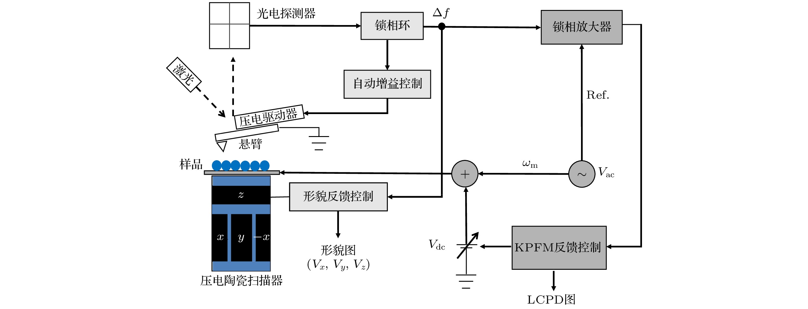
图 1 NC-AFM / FM-KPFM的实验原理图(浅灰色框是 NC-AFM 形貌部分, 深灰色框是 KPFM 部分)
Fig. 1. Schematic of NC-AFM/KPFM experiment (Light gray boxes are the NC-AFM topography part and the dark grey boxes are the KPFM part).
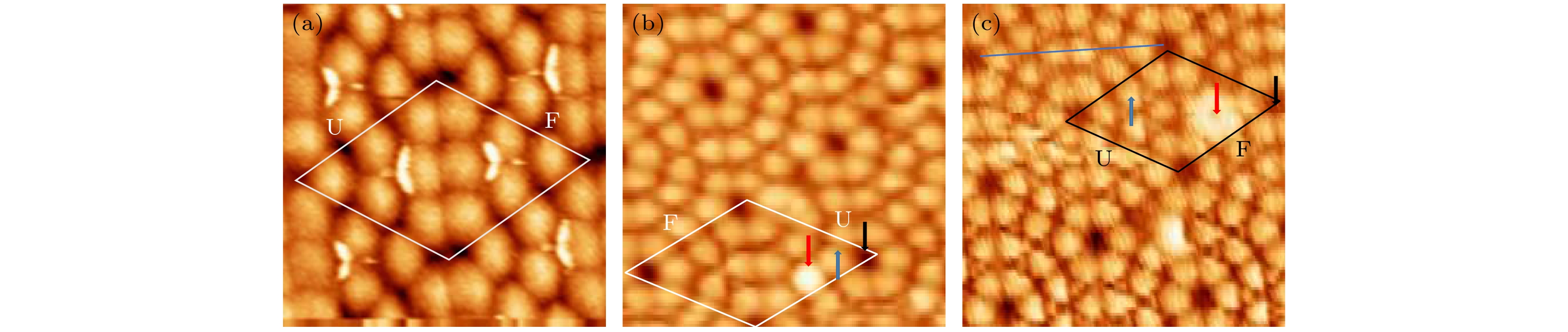
图 3 AFM 形貌图 (a) Si(111)-(7×7)表面, 图像尺寸为4.5 nm×2.5 nm (f0 = 162 kHz, Q = 1638, Δf = –45 Hz, A = 7 nm); (b) Au原子吸附在Si(111)-(7×7) 表面, 图像尺寸为5.3 nm×5.5 nm (f0 = 151 kHz, Q = 15011, Δf = –45 Hz, A = 7 nm); (c) Au 团簇吸附在Si(111)-(7×7) 表面, 图像尺寸为6.5 nm × 5.5 nm (f0 = 151 kHz, Q = 15011, Δf = –33.1 Hz, A = 7 nm)
Fig. 3. AFM images: (a) Si(111)-(7×7) surface, image size of 4.5 nm×2.5 nm (f0 = 162 kHz, Q = 1638, Δf = –45 Hz, A = 7 nm); (b) Au atoms adsorbed on Si(111)-(7×7) surface, image size of 5.3 nm×5.5 nm (f0 = 151 kHz, Q = 15011, Δf = –45 Hz, A = 7 nm); (c) Au cluster adsorbed on Si(111)-(7×7) surface , image size of 6.5 nm×5.5 nm (f0 = 151 kHz, Q = 15011, Δf = –33.1 Hz, A = 7 nm)
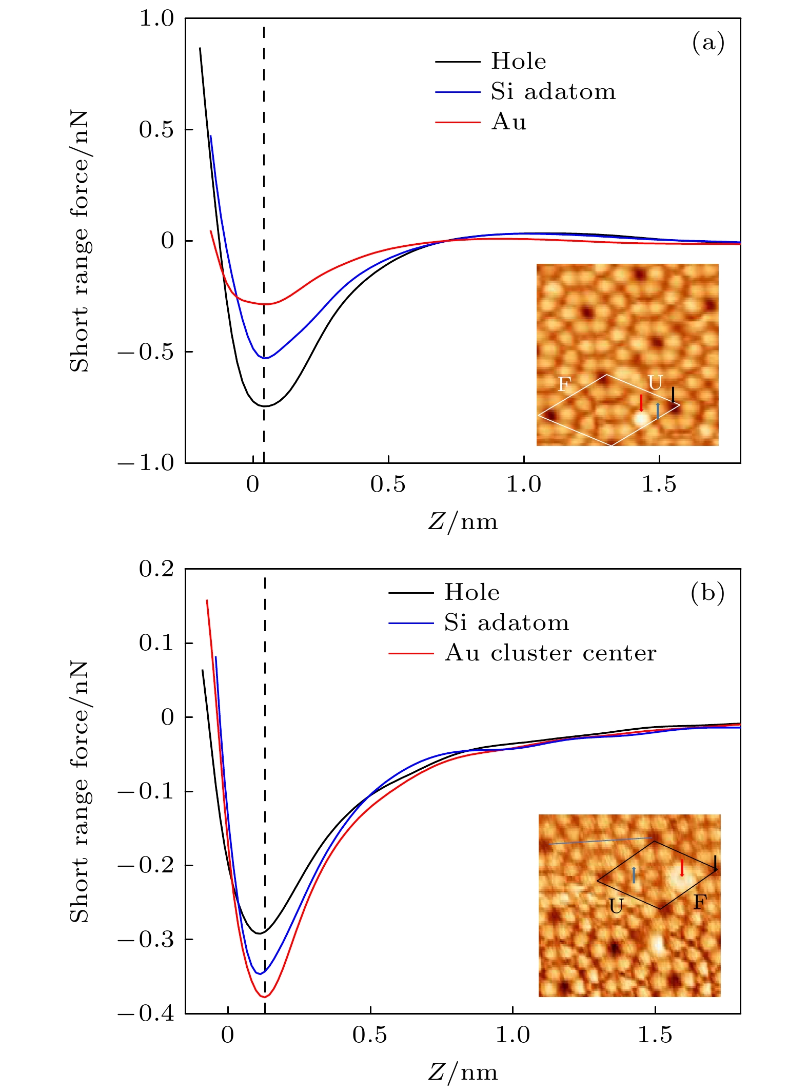
图 4 (a) Au/Si(111)-(7×7) 表面特定原子位置(图3(b))测量的短程力曲线, 箭头和绘图线的颜色代表相同; (b) Au团簇/Si(111)-(7×7) 表面特定原子位置(图3(c))测量的短程力曲线
Fig. 4. (a) Short range force curves measured over the atomic positions (Fig.3(b)) of Au/Si(111)-(7×7) surfces. The color code for arrows and plot lines is the same; (b) short range force curves measured over the atomic positions (Fig.3(c)) of Au cluster/Si(111)-(7×7) surfaces.
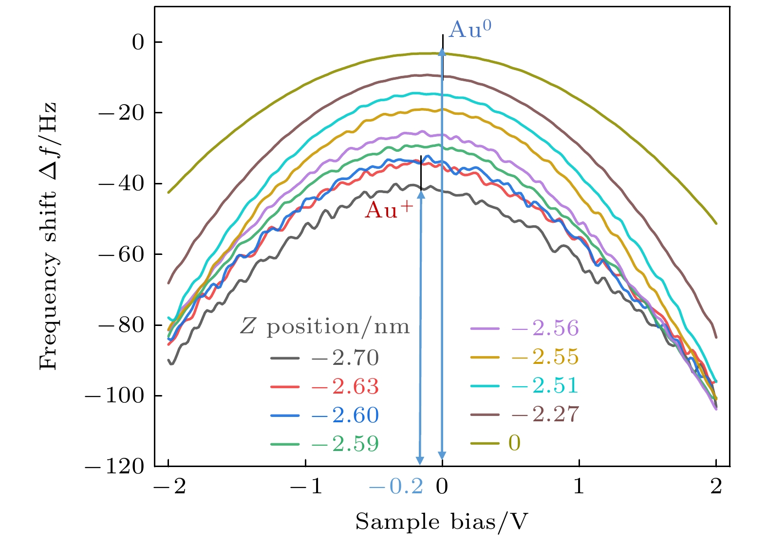
图 5 在不同针尖-样品表面距离下测得的探针本征频率频移与样品所加偏压关系曲线. 偏压值为0 V该处原子为中性金原子Au0; 偏压值为–0.2 V该处原子为带正电金原子Au+(以Δf = –4 Hz测量为起始点, 标记为Z = 0)
Fig. 5. Bias-spectroscopy curves measured at several tip surface separations to extract the bias voltage that minimizes the tip-surface electrostatic interaction. The bias value is 0 V, the atom is the neutral Au atom(Au0); bias value is –0.2 V, where the atom is a positively charged Au atom (Au+) (Starting point with Δf = –4 Hz measurement, marked as Z= 0)
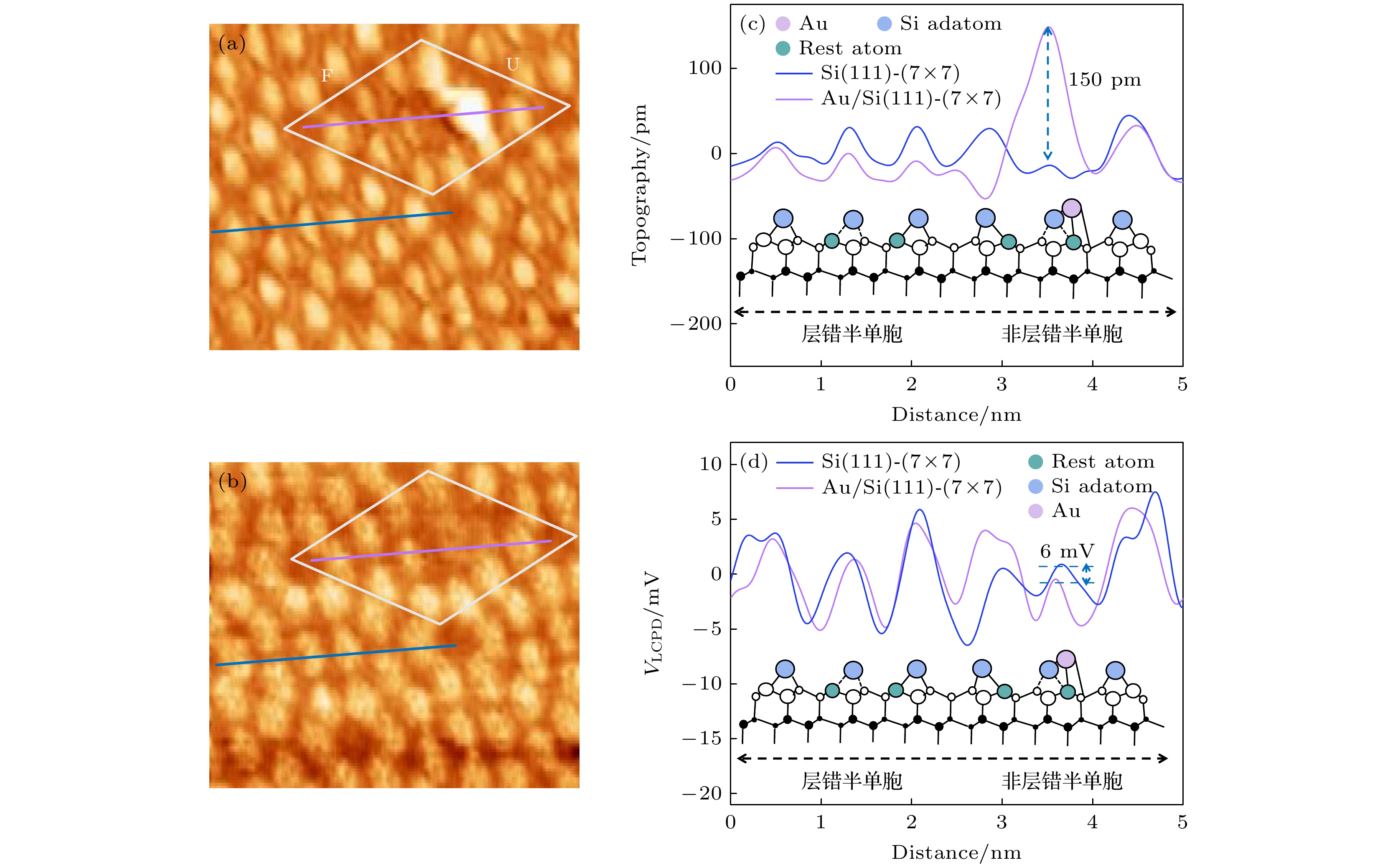
图 6 单个Au原子吸附在Si(111)-(7×7) 表面的 (a) 形貌图和 (b) VLCPD 图, 图像尺寸为6.5 nm×5 nm (f0 =151 kHz, Q = 15011, Δf = –66.2 Hz, A = 7 nm,
$ {V}_{{\rm{a}}{\rm{c}}} $ = 500 mV,$ {f}_{{\rm{a}}{\rm{c}}} $ = 500 Hz); (c) 形貌和 (d) VLCPD图的剖线图Fig. 6. (a) Topography and (b) VLCPD image of Au atoms absorbed on Si(111)-(7×7) surface, image size: 6.5 nm×5 nm (f0 = 151 kHz, Q = 15011, Δf = –66.2 Hz, A = 7 nm,
$ {V}_{{\rm{a}}{\rm{c}}} $ = 500 mV,$ {f}_{{\rm{a}}{\rm{c}}} $ = 500 Hz); (c) topography and (d) line profiles of VLCPD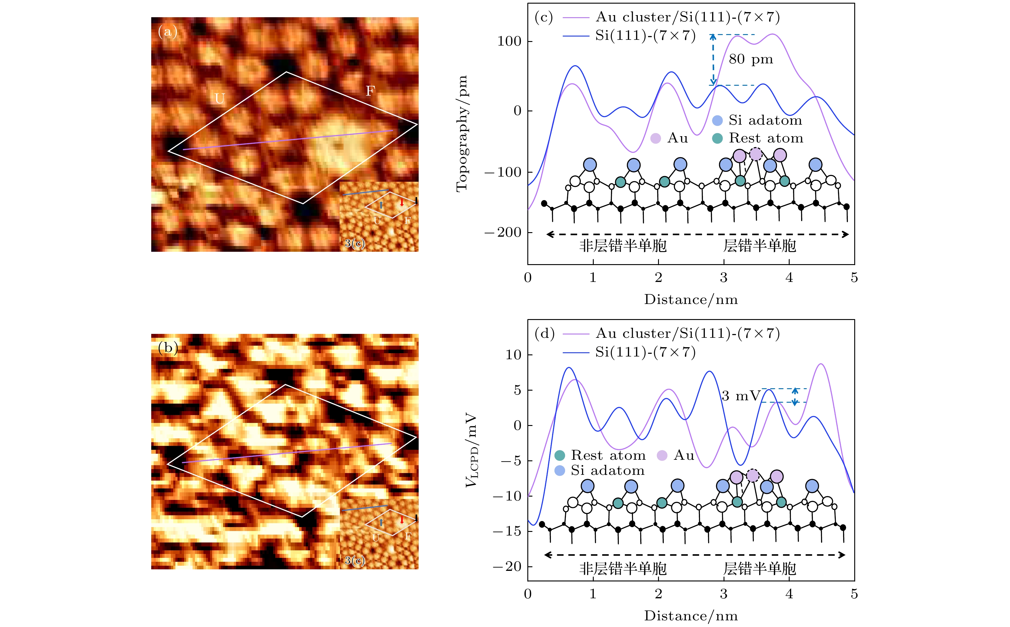
图 7 Au 团簇在Si (111)-(7×7) 表面的 (a) 形貌图和(b) VLCPD 图, 图像尺寸为 4.8 nm×2.5 nm (f0 = 151 kHz, Q = 15011, Δf = –33.1 Hz, A = 7 nm,
${V}_{\rm ac}$ = 500 mV,${f}_{{\rm{ac}}}$ = 500 Hz); (c) 形貌和 (d) VLCPD图的剖线图(图7选取自图3(a)中的部分图像, 图7中的蓝色线标注在图3(a)中, 紫色虚线圆圈为侧视图中的Au原子, 并不是截线位置上的Au原子)Fig. 7. (a) Topography and (b) VLCPD image of Au cluster absorbed on Si (111)-(7×7) surface, image size of 4.8 nm×2.5 nm (f0 = 151 kHz, Q = 15011, Δf = –33.1 Hz, A = 7 nm,
$ {V}_{{\rm{a}}{\rm{c}}} $ = 500 mV,$ {f}_{{\rm{a}}{\rm{c}}} $ = 500 Hz); (c) topography and (d) line profiles of VLCPD. (Fig.7 is selected from some of the images in Fig. 3(a), and the blue line in Fig.7 is denoted in Fig. 3(a), the purple dotted circle is the Au atom in the side view, not the Au atom in the truncated position).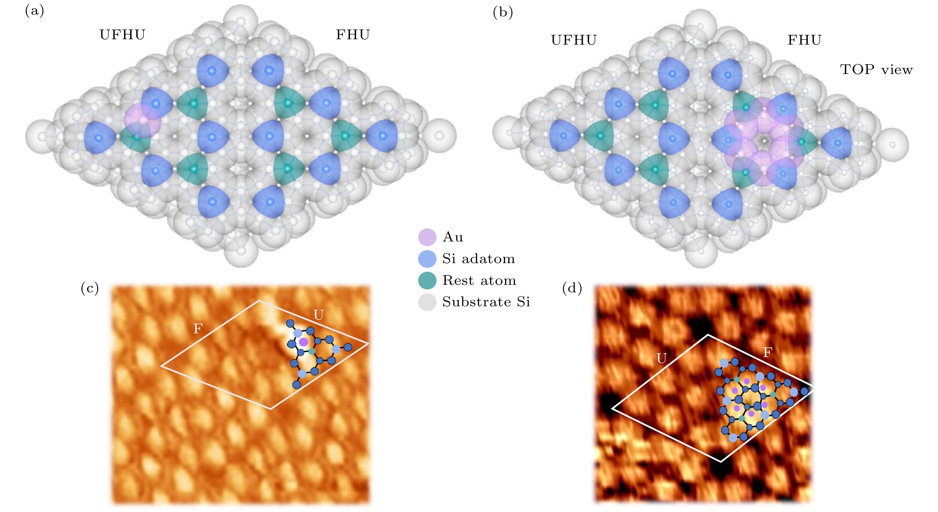
图 8 (a) Si (111)-(7×7)表面的单个Au原子模型, (b) Si (111)-(7×7)表面的Au团簇模型(灰色和蓝色球是表面的亚表面Si原子和Si顶戴原子, 绿色球是剩余原子, 紫色球是Au原子); (c) Au原子和(d) Au团簇吸附位置在对应AFM图上的示意图
Fig. 8. (a) Model of Au atoms absorbed on Si (111)-(7×7) surface, (b) model of Au cluster absorbed on Si (111)-(7×7) surface (the gray and blue balls are subsurface Si atoms and Si adatoms on the surface, the green balls are rest atoms, the pink balls are Au atoms); Schematic of adsorption position on the corresponding AFM images of (c) Au atoms and (d) Au cluster.
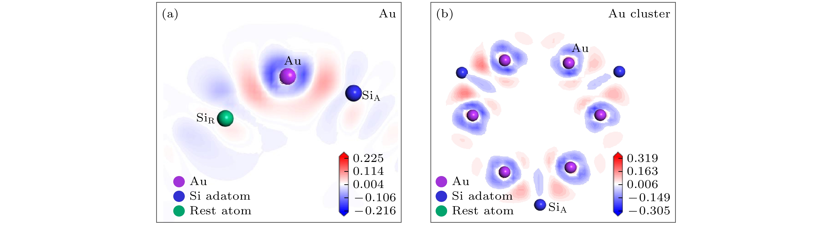
图 9 (a) 吸附在Si(111)-(7×7)表面高配位上的Au原子差分电荷密度分布; (b)吸附在Si (111)-(7×7)表面Au团簇的差分电荷密度分布
Fig. 9. (a) Differential charge density distribution of Au atom adsorbed on the high coordination of Si (111)-(7×7) surface; (b) differential charge density distribution of Au cluster adsorbed on Si (111)-(7×7) surface.
-
[1] Bocquet F, Nony L, Loppacher C, Glatzel T 2008 Phys. Rev. B 78 035410
Google Scholar
[2] Abraham D W, Williams C, Slinkman J, Wickramasinghe H K 1991 J. Vac. Sci. Technol. B 9 703
Google Scholar
[3] 温焕飞, 菅原康弘, 李艳君 2020 物理学报 69 210701
Google Scholar
Wen H F, Sugawara Y, Li Y J 2020 Acta Phys. Sin. 69 210701
Google Scholar
[4] Wen H F, Li Y J, Arima E, Naitoh Y, Sugawara Y, Xu R, Cheng Z H 2017 Nanotechnology 28 105704
Google Scholar
[5] Wen H F, Miyazaki M, Zhang Q, Adachi Y, Li Y J, Sugawara Y 2018 Phys. Chem. Chem. Phys. 20 28331
Google Scholar
[6] Ma Z M, Shi Y B, Mu J L, Qu Z, Zhang X M, Li Q, Liu J 2017 Appl. Surf. Sci. 394 472
Google Scholar
[7] Jia J F, Wang J Z, Liu X, Xue Q K, Li Z Q, Kawazoe Y, Zhang S B 2002 Appl. Phys. Lett. 80 3186
Google Scholar
[8] Wu K, Fujikawa Y, Nagao T, Hasegawa Y, Nakayama K S, Xue Q K, Wang E G, Briere T, Kumar V, Kawazoe Y, Zhang S B, Sakurai T 2003 Phys. Rev. Lett. 91 126101
Google Scholar
[9] Hu L, Huang B, Liu F 2021 Phys. Rev. Lett. 126 176101
Google Scholar
[10] Arai T, Inamura R, Kura D, Tomitori M 2018 Phys. Rev. B 97 115428
Google Scholar
[11] Tanishiro Y, Takahashi M, Takahashi S 1985 J. Vac. Sci. Technol. A 3 1502
Google Scholar
[12] Zhang L, Jeon Y J, Shim H, Lee G 2012 J. Vac. Sci. Technol. A 30 061406
Google Scholar
[13] Qu B , Hu J H, Li H, Li W J, Huang M L, Wu Q H 2015 Surf. Interface Anal. 47 926
Google Scholar
[14] Liu Q, Fu Q, Shao X J, Ma X H, Wu X F, Wang K D, Xiao X D 2017 Appl. Surf. Sci. 401 225
Google Scholar
[15] Li W, Ding W, Gong Y, Ju D 2021 Surface. Coatings 11 281
Google Scholar
[16] Baranov D S, Vlaic S, Baptista, J, Cofler E, Stolyarov V S, Roditchev D, Pons S 2022 Nano. Lett. 22 652
Google Scholar
[17] 王慧云 冯婕 王旭东 温阳 魏久焱 温焕飞 石云波 马宗敏 李艳君 刘俊 2022 物理学报 71 060702
Google Scholar
Wang H Y, Feng J, Wang X D, Wen Y, Wei J Y, Wen H F, Shi Y B, Ma Z M, Li Y J, Liu Jun 2022 Acta Phys. Sin. 71 060702
Google Scholar
[18] 周颖慧 2007 博士学位论文 (厦门: 厦门大学)
Zhou Y H 2007 Ph. D. Dissertation(Xiamen: Xiamen University) (in Chinese)
[19] 魏久焱 马宗敏 温焕飞 2020 电子显微学报 39 122
Google Scholar
Wei J Y, Ma Z M, Wen H F 2020 J. Chin. Electron Microsc. Soc. 39 122
Google Scholar
[20] Yurtsever A, Sugimoto Y, Tanaka H, Abe M, Morita S, Ondrác M, Pou P, Pérez R, Jelínek P 2013 Phys. Rev. B 87 155403
Google Scholar
[21] Pou P, Ghasemi S A, Jelinek P, Lenosky T, Goedecker S, Perez R 2009 Nanotechnology 20 264015
Google Scholar
[22] Chen G, Xiao X D, Kawazoe Y, Gong X G, Chan C T 2009 Phys. Rev. B 79 115301
Google Scholar
[23] Wandelt K 1997 Appl. Surf. Sci. 111 1
Google Scholar
[24] Gross L, Mohn F, Liljeroth P, Repp J, Giessibl F J, Meyer G 2009 Science 324 1428
Google Scholar
[25] Huang Z, Lin Y, Han C, Han C, Sun Y Y, Wu K, Chen E 2021 J. Phys. Chem. C 125 7944
Google Scholar
[26] Zhou Y H, Wu Q H, Li S P, Kang J Y 2007 Surf. Rev. Lett. 14 657
Google Scholar

 下载:
下载:


计量
- 文章访问数: 5791
- PDF下载量: 108
- 被引次数: 0
