


-
单层CuSe属于体相为非层状的二维材料, 本质上具有金属性质, 因此不适合在电子器件中应用. 本文通过外部原子修饰的方法实现CuSe电子结构的改变, 采用密度泛函理论的第一性原理研究了单层CuSe在顶位、中心和桥位添加第二周期原子后的能带结构, 重点分析了单层CuSe添加Li和B原子的电子结构, 包括能带结构、态密度、差分电荷密度和晶体轨道哈密顿布居分析. 添加Li原子后, 从能带结构的结果来看, 三个位置都能实现CuSe由金属性转为半导体性, 且Li原子更倾向修饰在CuSe的六角形中心, 带隙约为1.77 eV; 在Cu原子的顶部位置添加B原子也可以实现CuSe具有半导体性, 带隙约为1.2 eV. 通过差分电荷密度和晶体轨道哈密顿布居的结果来看, B原子用B-Se极性共价键结合在单层CuSe的顶部. 第一原理揭示了从单层CuSe到CuXSe (X = Li, B)的金属到半导体转变的实现, 计算结果使CuSe在未来的电子设备中使用成为可能.Original bulk phases of two-dimensional atomic crystal materials are layered. However, a few relevant researches show that some of two-dimensional material crystals have non-layered bulk phases. In this work we investigate monolayer CuSe which is non-layered, belonging in a new kind of honeycomb graphene analogue. Monolayer CuSe is not suitable for application in electronic devices because of its metallic nature. In order to find new two-dimensional atomic crystal materials with excellent performance suitable for application in electronic devices, we change CuSe from metal to semiconductor through external atom modification. The first principles study of density functional theory is conducted to ascertain the energy band structure of monolayer CuSe after second periodic atoms have been added to the top, center and bridge sites. The characteristics of monolayer CuSe with addition of Li or B atoms are studied, including energy band structure, the density of states, differential charge density, and crystal orbital Hamiltonian population. The results show that after adding Li atoms to CuSe, the CuSe transforms from metallic to semiconductive property at all three positions, and Li atom is more easily to be modified in the hexagonal center of CuSe, with band gap being about 1.77 eV, the Fermi level biased towards the top of the valence band. The CuSe with addition of Li atoms exhibits a p-type semiconductor property, so it is a direct bandgap semiconductor. Adding B atom to the top of Cu atom can also make CuSe semiconductive, with a band gap of about 1.2 eV, the conduction band minimum at the K point, and the valence band maximum at the Γ point. The CuSe with addition of B atoms belongs in an indirect band gap semiconductor, and the Fermi energy level is biased towards the conduction band minimum, exhibiting the characteristics of an n-type semiconductor. According to the results of differential charge density and crystal orbital Hamiltonian population, the B atom is bound to the top of the monolayer CuSe with the B-Se polar covalent bond. The first principle study reveals the realization of metal-to-semiconductor transition from monolayer CuSe to CuXSe (X = Li, B), and the calculation results also show that CuSe with addition of Li atoms or B atoms is likely to be used in future electronic devices.
-
Keywords:
- monolayer CuSe /
- first-principles calculations /
- electronic structure
[1] Novoselov K S, Geim A K, Morozov S V, Jiang D, Zhang Y, Dubonos S V, Grigorieva I V, Firsov A A 2004 Science 306 666
 Google Scholar
[2] Zhao J J, Liu H S, Yu Z M, Quhe R, Zhou S, Wang Y Y, Liu C C, Zhong H X, Han N N, Lu J, Yao Y G, Wu K H 2016 Prog. Mater. Sci. 83 24
Google Scholar
[3] Lang J L, Ding B, Zhang S, Su H X, Ge B H, Qi L H, Gao H J, Li X Y, Li Q Y, Wu H 2017 Adv. Mater. 29 1701777
Google Scholar
[4] Feng B J, Ding Z J, Meng S, Yao Y G, He X Y, Cheng P, Chen L, Wu K H 2012 Nano Lett. 12 3507
Google Scholar
[5] Liao Y L, Chen Z F, Connell J W, Fay C C, Park C, Kim J W, Lin Y 2014 Adv. Funct. Mater. 24 4497
Google Scholar
[6] Zeng H B, Zhi C Y, Zhang Z H, Wei X L, Wang X B, Guo W L, Bando Y, Golberg D 2010 Nano Lett. 10 5049
Google Scholar
[7] Kumar R, Sahoo S, Joanni E, Singh R K, Yadav R M, Verma R K, Singh D P, Tan W K, Pino A P, Moshkalev S A, Matsuda A 2019 Nano Res. 12 2655
Google Scholar
[8] Splendiani A, Sun L, Zhang Y B, Li T S, Kim J, Chim C Y, Galli G, Wang F 2010 Nano Lett. 10 1271
Google Scholar
[9] Mak K F, Lee C, Hone J, Shan J, Heinz T F 2010 Phys. Rev. Lett. 105 136805
Google Scholar
[10] Chhowalla M, Liu Z F, Zhang H 2015 Chem. Soc. Rev. 44 2584
Google Scholar
[11] Naguib M, Kurtoglu M, Presser V, Lu J, Niu J J, Heon M, Hultman L, Gogotsi Y, Barsoum M W 2011 Adv. Mater. 23 4248
Google Scholar
[12] Naguib M, Mashtalir O, Carle J, Presser V, Lu J, Hultman L, Gogotsi Y, Barsoum M W 2012 Acs Nano 6 1322
Google Scholar
[13] Zhan X X, Si C, Zhou J, Sun Z M 2020 Nano. Horiz. 5 235
Google Scholar
[14] Aydın Z Y, Abacı S 2017 Solid State Sci. 74 74
Google Scholar
[15] Buffiere M, Dhawale D S, EI-Mellouhi F 2019 Energy Technol. 7 1900819
Google Scholar
[16] Yang Z Q, Wang S C, Li H L, Yang J P, Zhao J X, Qu W Q, Shih K 2020 Ind. End. Chem. Res. 59 13603
Google Scholar
[17] Masrat S, Poolla R, Dipak P, Zaman M B 2021 Surf. Interfaces 23 100973
Google Scholar
[18] Cheng Y S, Zhang J, Xiong X S, Chen C, Zeng J H, Kong Z, Wang H B, Xi J H, Yuan Y J, Ji Z G 2021 J. Alloy. Compd. 870 159540
Google Scholar
[19] Weng J H, Gao S P 2019 Rsc. Adv. 9 32984
Google Scholar
[20] Weng J H, Gao S P 2021 J. Phys. Chem. Solids 148 109738
Google Scholar
[21] Yang G, Xu W X, Gao S P 2021 Comput. Mater. Sci. 198 110696
Google Scholar
[22] Ruffieux P, Wang S Y, Yang B, Sanchez-Sanchez C, Liu J, Dienel T, Talirz L, Shinde P, Pignedoli C A, Passerone D, Dumslaff T, Feng X L, Mullen K, Fasel R 2016 Nature 531 489
Google Scholar
[23] Nakanishi T, Ando T 2015 Phys. Rev. B 91 155420
Google Scholar
[24] Chamlagain B, Withanage S S, Johnston A C, Khondaker S I 2020 Sci. Rep. 10 12970
Google Scholar
[25] Cao T, Li Z L, Louie S G 2015 Phys. Rev. Lett. 114 236602
Google Scholar
[26] Kang M G, Kim B, Ryu S H, Jung S W, Kim J, Moreschini L, Jozwiak C, Rotenberg E, Bostwick A, Kim K S 2017 Nano Lett. 17 1610
Google Scholar
[27] Dai Z H, Liu L Q, Zhang Z 2019 Adv. Mater. 31 1805417
Google Scholar
[28] Cui X, Lee G H, Kim Y D, Arefe G, Huang P Y, Lee C H, Chenet D A, Zhang X, Wang L, Ye F, Pizzocchero F, Jessen B S, Watanabe K, Taniguchi T, Muller D A, Low T, Kim P, Hone J 2015 Nat. Nanotech. 10 534
Google Scholar
[29] Ju L, Shi Z W, Nair N, Lü Y C, Jin C H, Jr J V, Ojeda-Aristizabal C, Bechtel H A, Martin M C, Zettl A, Analytis J and Wang F 2015 Nature 520 650
Google Scholar
[30] Lebegue S, Klintenberg M, Eriksson O, Katsnelson M I 2009 Phys. Rev. B 79 245117
Google Scholar
[31] Yang J H, Song S R, Du S X, Gao H J, Yakobson B I 2017 J. Phys. Chem. Lett. 8 4594
Google Scholar
[32] Wang Q C, Lei Y P, Wang Y C, Liu Y, Song C Y, Zeng J, Song Y H, Duan X D, Wang D S, Li Y D 2020 Energy Environ. Sci. 13 1593
Google Scholar
[33] Kresse G, Furthmüller J 1996 Phys. Rev. B 54 11169
Google Scholar
[34] Perdew J P, Burke K, Ernzerhof M 1996 Phy. Rev. Lett. 77 3865
Google Scholar
[35] Wu X J, Huang X, Liu J Q, Li H, Yang J, Li B, Huang W, Zhang H 2014 Angew. Chem. 126 5183
Google Scholar
-

图 1 CuBSe不同位置的晶体结构俯视图 (a) B在Cu的顶位; (b) B在Se的顶位; (c) B在中心位置; (d) B在桥位
Fig. 1. Top view of crystal structure at different positions of CuBSe: (a) B is at the top of Cu; (b) B is at the top of Se; (c) B in the center; (d) B at bridge site.
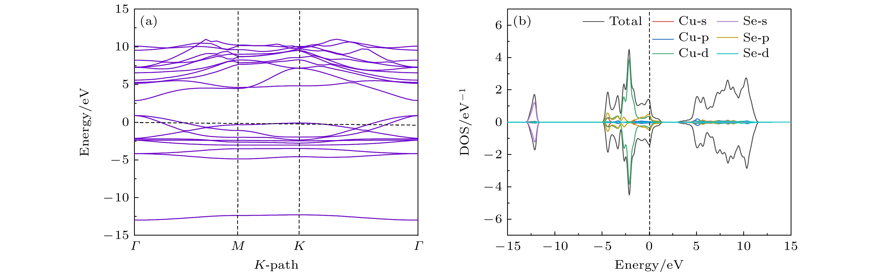
图 2 单层CuSe的电子结构 (a) 单层CuSe的能带结构; (b) 单层CuSe的态密度
Fig. 2. Electronic structure of monolayer CuSe: (a) Energy band structure of monolayer CuSe; (b) density of states of monolayer CuSe.

图 3 CuXSe (X = Li, Be, B, C, N, O, F)的能带结构 (a)—(c), (d)—(f), (g)—(i), (j)—(l), (m)—(o), (p)—(r), (s)—(u) 依次表示Li, Be, B, C, N, O, F原子分别在CuSe的顶部位置、中心位置和桥位
Fig. 3. Energy band structure of CuXSe (X = Li, Be, B, C, N, O, F): (a)–(c), (d)–(f), (g)–(i), (j)–(l), (m)–(o), (p)–(r), (s)–(u) Indicate the top position, center position, and bridge position of Li, Be, B, C, N, O and F atoms in CuSe in sequence.

图 4 CuLiSe (Li在CuSe的顶部) (a) 态密度图; (b) Fermi能级附近放大图
Fig. 4. CuLiSe (Li at the top of CuSe): (a) Density of states diagram; (b) enlarged view near Fermi energy level.

图 5 CuLiSe (Li在CuSe的桥位) (a) 态密度图; (b) Fermi能级附近放大图
Fig. 5. CuLiSe (Li bridge site in CuSe): (a) Density of states diagram; (b) enlarged view near Fermi energy level.
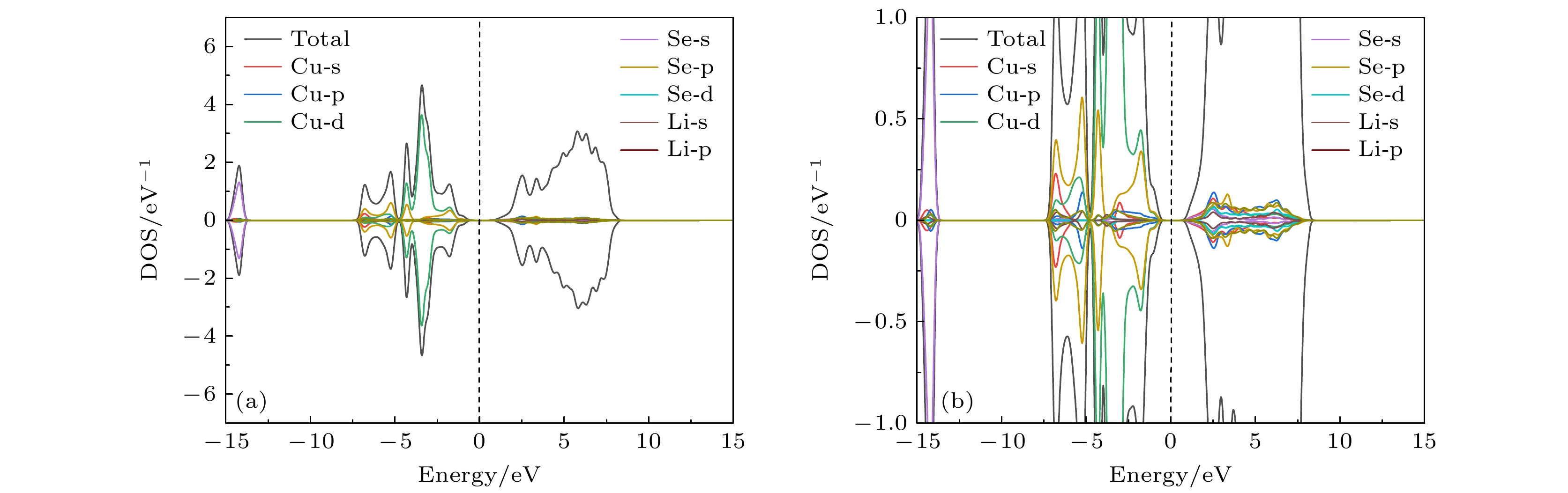
图 6 CuLiSe (Li在CuSe的中心) (a) 态密度图; (b) Fermi能级附近放大图
Fig. 6. CuLiSe (Li is in the center of CuSe): (a) Density of states diagram; (b) enlarged view near Fermi energy level.
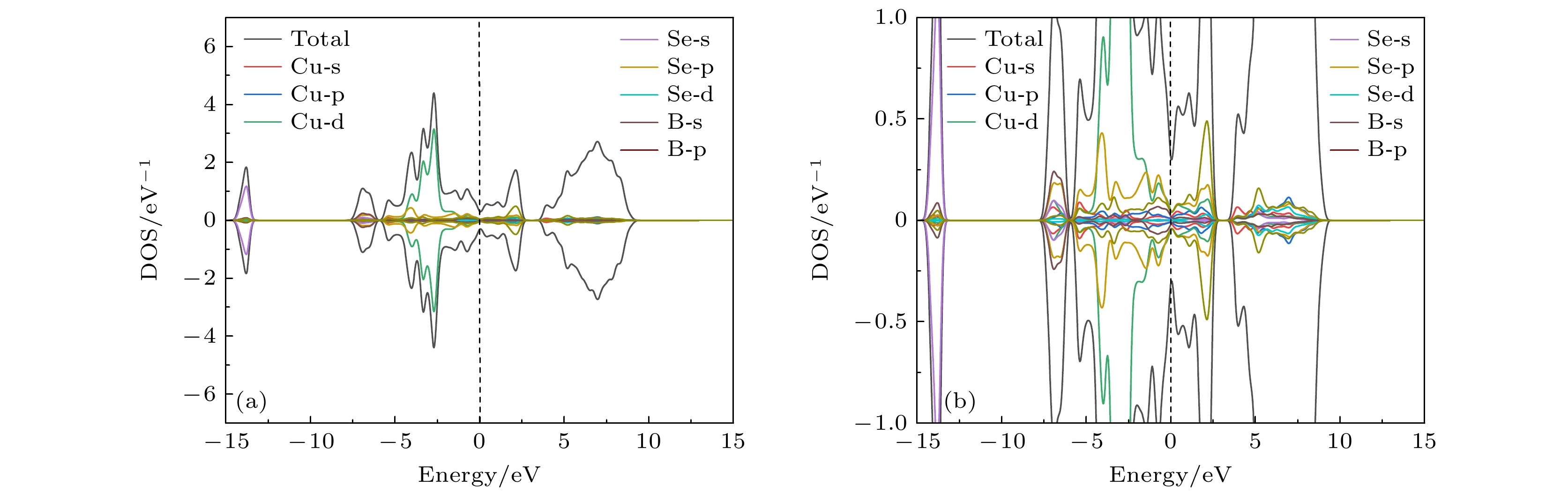
图 7 CuBSe (B在CuSe的顶部) (a) 态密度图; (b) Fermi能级附近放大图
Fig. 7. CuBSe (B at the top of CuSe): (a) Density of states diagram; (b) enlarged view near Fermi energy level.
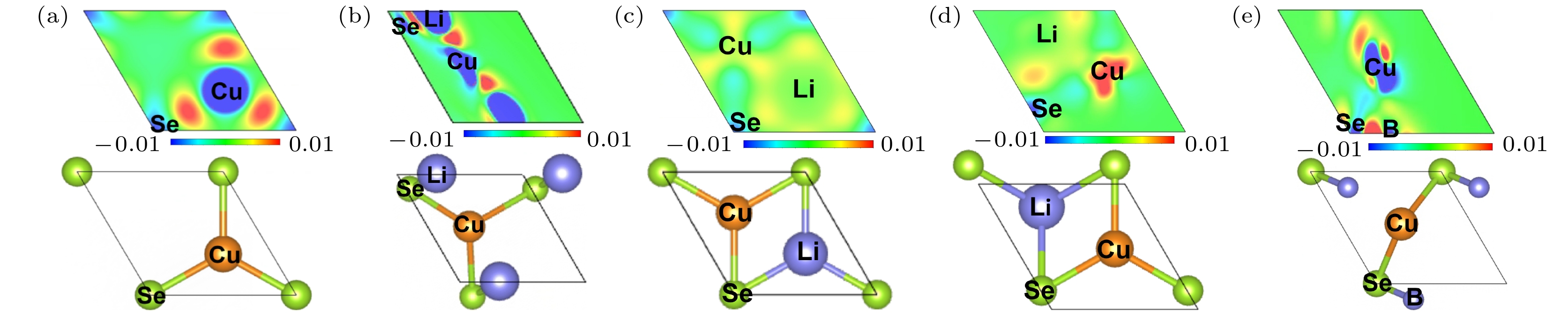
图 8 差分电荷密度图及对应的结构图 (a) CuSe; (b)—(d) CuLiSe (Li分别在CuSe的顶部位置、中心位置和桥位); (e) CuBSe (B在CuSe的顶部位置)
Fig. 8. Differential charge density diagram and corresponding crystal structure: (a) CuSe; (b)−(d) CuLiSe (Li at the top, center and brdige position of CuSe); (e) CuBSe (B at the top of CuSe).

图 9 CuLiSe (Li在CuSe的中心)的COHP图 (a) Se-Cu; (b) Li-Se; (c) Li-Cu
Fig. 9. COHP diagram of CuLiSe (Li in the center of CuSe): (a) Se-Cu; (b) Li-Se; (c) Li-Cu.
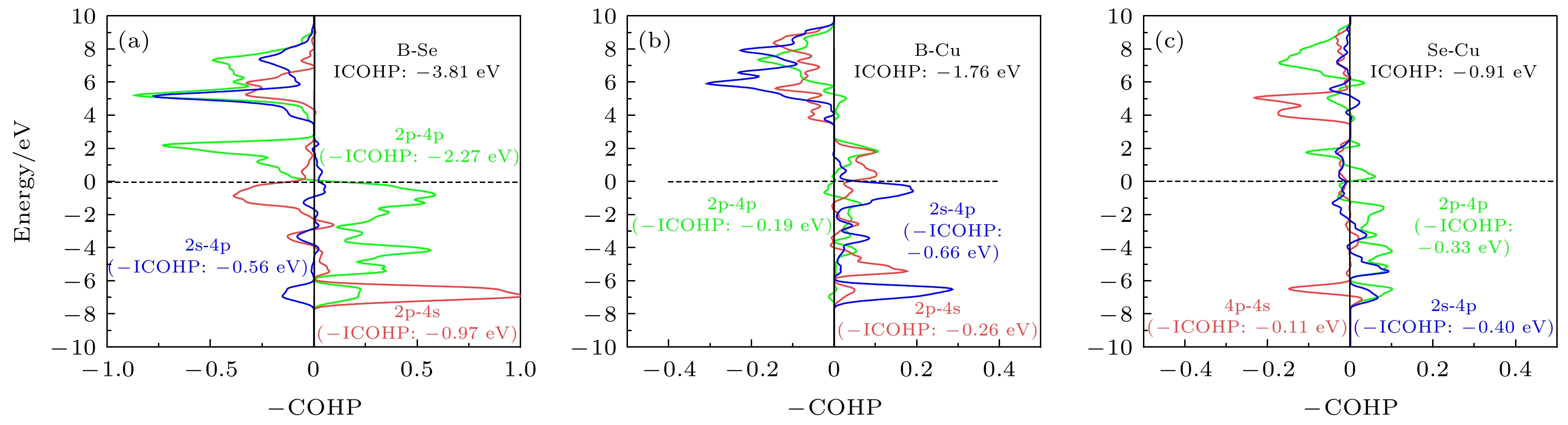
图 10 CuBSe (B在CuSe的顶部)的COHP图 (a) B-Se; (b) B-Cu; (c) Se-Cu
Fig. 10. COHP diagram of CuBSe (B at the top of CuSe): (a) B-Se; (b) B-Cu; (c) Se-Cu.
表 1 CuXSe (X = Li, Be, B, C, N, O, F)体系不同位置的形成能
Table 1. Formation energy at different positions of CuXSe (X = Li, Be, B, C, N, O, F)system.
掺杂体系 不同位置的形成能$ {E}_{{\rm{f}}} $/eV Cu原子的顶位 Se原子的顶位 中心位置 桥位 最稳定的位置 CuLiSe –2.016 –1.747 –2.622 –2.257 中心位置 CuBeSe –2.456 –1.979 –2.091 –2.520 桥位 CuBSe –3.509 –3.723 –2.484 –2.121 Se原子的顶位 CuCSe –4.291 –4.212 –2.619 –2.452 Cu原子的顶位 CuNSe –0.860 –1.647 –1.044 –1.532 Se原子的顶位 CuOSe –3.271 –2.977 –1.704 –2.177 Cu原子的顶位 CuFSe –2.537 –2.737 –1.398 –2.087 Se原子的顶位  下载: 导出CSV
-
[1] Novoselov K S, Geim A K, Morozov S V, Jiang D, Zhang Y, Dubonos S V, Grigorieva I V, Firsov A A 2004 Science 306 666
Google Scholar
[2] Zhao J J, Liu H S, Yu Z M, Quhe R, Zhou S, Wang Y Y, Liu C C, Zhong H X, Han N N, Lu J, Yao Y G, Wu K H 2016 Prog. Mater. Sci. 83 24
Google Scholar
[3] Lang J L, Ding B, Zhang S, Su H X, Ge B H, Qi L H, Gao H J, Li X Y, Li Q Y, Wu H 2017 Adv. Mater. 29 1701777
Google Scholar
[4] Feng B J, Ding Z J, Meng S, Yao Y G, He X Y, Cheng P, Chen L, Wu K H 2012 Nano Lett. 12 3507
Google Scholar
[5] Liao Y L, Chen Z F, Connell J W, Fay C C, Park C, Kim J W, Lin Y 2014 Adv. Funct. Mater. 24 4497
Google Scholar
[6] Zeng H B, Zhi C Y, Zhang Z H, Wei X L, Wang X B, Guo W L, Bando Y, Golberg D 2010 Nano Lett. 10 5049
Google Scholar
[7] Kumar R, Sahoo S, Joanni E, Singh R K, Yadav R M, Verma R K, Singh D P, Tan W K, Pino A P, Moshkalev S A, Matsuda A 2019 Nano Res. 12 2655
Google Scholar
[8] Splendiani A, Sun L, Zhang Y B, Li T S, Kim J, Chim C Y, Galli G, Wang F 2010 Nano Lett. 10 1271
Google Scholar
[9] Mak K F, Lee C, Hone J, Shan J, Heinz T F 2010 Phys. Rev. Lett. 105 136805
Google Scholar
[10] Chhowalla M, Liu Z F, Zhang H 2015 Chem. Soc. Rev. 44 2584
Google Scholar
[11] Naguib M, Kurtoglu M, Presser V, Lu J, Niu J J, Heon M, Hultman L, Gogotsi Y, Barsoum M W 2011 Adv. Mater. 23 4248
Google Scholar
[12] Naguib M, Mashtalir O, Carle J, Presser V, Lu J, Hultman L, Gogotsi Y, Barsoum M W 2012 Acs Nano 6 1322
Google Scholar
[13] Zhan X X, Si C, Zhou J, Sun Z M 2020 Nano. Horiz. 5 235
Google Scholar
[14] Aydın Z Y, Abacı S 2017 Solid State Sci. 74 74
Google Scholar
[15] Buffiere M, Dhawale D S, EI-Mellouhi F 2019 Energy Technol. 7 1900819
Google Scholar
[16] Yang Z Q, Wang S C, Li H L, Yang J P, Zhao J X, Qu W Q, Shih K 2020 Ind. End. Chem. Res. 59 13603
Google Scholar
[17] Masrat S, Poolla R, Dipak P, Zaman M B 2021 Surf. Interfaces 23 100973
Google Scholar
[18] Cheng Y S, Zhang J, Xiong X S, Chen C, Zeng J H, Kong Z, Wang H B, Xi J H, Yuan Y J, Ji Z G 2021 J. Alloy. Compd. 870 159540
Google Scholar
[19] Weng J H, Gao S P 2019 Rsc. Adv. 9 32984
Google Scholar
[20] Weng J H, Gao S P 2021 J. Phys. Chem. Solids 148 109738
Google Scholar
[21] Yang G, Xu W X, Gao S P 2021 Comput. Mater. Sci. 198 110696
Google Scholar
[22] Ruffieux P, Wang S Y, Yang B, Sanchez-Sanchez C, Liu J, Dienel T, Talirz L, Shinde P, Pignedoli C A, Passerone D, Dumslaff T, Feng X L, Mullen K, Fasel R 2016 Nature 531 489
Google Scholar
[23] Nakanishi T, Ando T 2015 Phys. Rev. B 91 155420
Google Scholar
[24] Chamlagain B, Withanage S S, Johnston A C, Khondaker S I 2020 Sci. Rep. 10 12970
Google Scholar
[25] Cao T, Li Z L, Louie S G 2015 Phys. Rev. Lett. 114 236602
Google Scholar
[26] Kang M G, Kim B, Ryu S H, Jung S W, Kim J, Moreschini L, Jozwiak C, Rotenberg E, Bostwick A, Kim K S 2017 Nano Lett. 17 1610
Google Scholar
[27] Dai Z H, Liu L Q, Zhang Z 2019 Adv. Mater. 31 1805417
Google Scholar
[28] Cui X, Lee G H, Kim Y D, Arefe G, Huang P Y, Lee C H, Chenet D A, Zhang X, Wang L, Ye F, Pizzocchero F, Jessen B S, Watanabe K, Taniguchi T, Muller D A, Low T, Kim P, Hone J 2015 Nat. Nanotech. 10 534
Google Scholar
[29] Ju L, Shi Z W, Nair N, Lü Y C, Jin C H, Jr J V, Ojeda-Aristizabal C, Bechtel H A, Martin M C, Zettl A, Analytis J and Wang F 2015 Nature 520 650
Google Scholar
[30] Lebegue S, Klintenberg M, Eriksson O, Katsnelson M I 2009 Phys. Rev. B 79 245117
Google Scholar
[31] Yang J H, Song S R, Du S X, Gao H J, Yakobson B I 2017 J. Phys. Chem. Lett. 8 4594
Google Scholar
[32] Wang Q C, Lei Y P, Wang Y C, Liu Y, Song C Y, Zeng J, Song Y H, Duan X D, Wang D S, Li Y D 2020 Energy Environ. Sci. 13 1593
Google Scholar
[33] Kresse G, Furthmüller J 1996 Phys. Rev. B 54 11169
Google Scholar
[34] Perdew J P, Burke K, Ernzerhof M 1996 Phy. Rev. Lett. 77 3865
Google Scholar
[35] Wu X J, Huang X, Liu J Q, Li H, Yang J, Li B, Huang W, Zhang H 2014 Angew. Chem. 126 5183
Google Scholar

 下载:
下载:
计量
- 文章访问数: 7764
- PDF下载量: 242
- 被引次数: 0
