


-
紫外探测器在火灾预警、导弹跟踪以及紫外线杀菌消毒的剂量检测方面有着很重要的作用, 与人类生活息息相关. 随着探测系统集成化的发展, 对探测器的尺寸、能耗等方面的要求越来越严格, 需要外加电源工作的传统探测器已经不能满足这样的要求. 于是本文提出了一种基于NiO/GaN p-n结的紫外探测器. 利用磁控溅射的方法, 在高质量的n-GaN膜上(由金属有机化学气相沉积生长在蓝宝石衬底上)沉积一层p-NiO, 构建了NiO/GaN p-n结, 在 ± 0.5 V下显示出明显的二极管整流特性. 利用结区产生的内建电场, 器件可以在没有外加偏压的条件下工作. 0 V下对365 nm的紫外光显示出272.3 mA/W的响应度以及高达2.83 × 1014 Jones的探测率. 得益于薄膜良好的结晶性, 暗电流低至10–10 A, 开关比 > 103, 同时响应速度达到31 ms. 这些优异的性能显示出了基于NiO/GaN p-n结的器件在紫外探测领域广阔的应用前景, 为未来智能化集成发展提供了新的思路.
Ultraviolet photodetector plays an important role in fire warning, missile tracking and dose detecting of ultraviolet sterilization and disinfection, which is closely related to human lives. With the development of integrated detection system, the requirements for the size and energy consumption of the detector are becoming more and more stringent. Traditional detector that requires an external power supply can no longer meet these requirements. Moreover, a traditional ultraviolet detector is mainly composed of first-generation semiconductors and second-generation semiconductors. These semiconductors have small band gaps and large cut-off wavelengths, and are more suitable for infrared detection. When used for implementing the ultraviolet detection, an additional layer is often required, which increases not only the volume but also the cost. Gallium nitride (GaN), as a third-generation semiconductor, has a band gap of 3.4 eV and a corresponding absorption edge of 365 nm. It is a natural ultraviolet detection material. At the same time, the excellent physical and chemical properties make the devices prepared by GaN have high stability. In recent years, some studies have shown that the GaN-based ultraviolet photodetectors have excellent responsiveness, but each of these detectors usually requires an external bias and has a slow response speed. Here, we propose a high responsivity, fast response speed and self-powered ultraviolet photodetector based on NiO/GaN p-n junction. By using the magnetron sputtering, a layer of 70 nm thick p-NiO film is deposited on a high-quality n-GaN film that has been grown on a sapphire substrate by the metal-organic chemical vapor deposition. The fabricated p-n junction shows obvious rectification characteristics at ± 0.5 V. Due to the existence of the built-in electric field, the device can work without externally applied bias. Under zero bias, the detector shows a responsivity of 272.3 mA/W for 365 nm ultraviolet light while the intensity is 50 μW/cm2, and has a detectivity as high as 2.83 × 10¹⁴ Jones. This indicates that the detector has a high sensitivity even for very weak light. Owing to the good crystallinity of the film, the dark current is as low as 10–10 A, the switching ratio is > 103, and the response speed reaches 31 ms. These excellent properties show the broad application prospects of the devices based on NiO/GaN p-n junctions in the field of self-powered ultraviolet detection, and thus providing new ideas for the future development of intelligent integration. -
Keywords:
- ultraviolet photodetector /
- self-powered technology /
- GaN /
- NiO
[1] Guo D, Chen K, Wang S, Wu F, Liu A, Li C, Li P, Tan C, Tang W 2020 Phys.Rev. Appl. 13 024051
 Google Scholar
[2] 郭道友, 李培刚, 陈政委, 吴真平, 唐为华 2019 物理学报 68 078501
Google Scholar
Guo D Y, Li P G, Chen Z W, Wu Z P, Tang W H 2019 Acta Phys. Sin. 68 078501
Google Scholar
[3] Wu C, He C, Guo D, Zhang F, Li P, Wang S, Liu A, Wu F, Tang W 2020 Mater. Today Phys. 12 100193
Google Scholar
[4] Guo D, Guo Q, Chen Z, Wu Z, Li P, Tang W 2019 Materials Today Physics 11 100157
Google Scholar
[5] Strite S, Morkoç H 1992 J. Vac. Sci. Technol., B 10 1237
Google Scholar
[6] Li J, Xi X, Lin S, Ma Z, Li X, Zhao L 2020 ACS Appl. Mater. Interfaces 12 11965
Google Scholar
[7] Wang W, Zheng Y, Li X, Li Y, Huang L, Li G 2018 J. Mater. Chem. C 6 3417
Google Scholar
[8] Lee J H, Lee W W, Yang D W, Chang W J, Kwon S S, Park W I 2018 ACS Appl. Mater. Interfaces 10 14170
Google Scholar
[9] Xiao Y, Zhang W G, Tan Z T, Pan G B, Peng Z 2020 Chem. Phys. Lett. 739 136981
Google Scholar
[10] Zhuo R, Wang Y, Wu D, Lou Z, Shi Z, Xu T, Xu J, Tian Y, Li X 2018 J. Mater. Chem. C 6 299
Google Scholar
[11] Guo D, Su Y, Shi H, Li P, Zhao N, Ye J, Wang S, Liu A, Chen Z, Li C, Tang W 2018 ACS Nano 12 12827
Google Scholar
[12] De Vittorio M, Potì B, Todaro M, Frassanito M, Pomarico A, Passaseo A, Lomascolo M, Cingolani R 2004 Sens. Actuators, A 113 329
Google Scholar
[13] Guo X, Williamson T, Bohn P 2006 Solid State Commun. 140 159
Google Scholar
[14] Su L, Zhang Q, Wu T, Chen M, Su Y, Zhu Y, Xiang R, Gui X, Tang Z 2014 Appl. Phys. Lett. 105 072106
Google Scholar
[15] Zhu Y, Liu K, Ai Q, Hou Q, Chen X, Zhang Z, Xie X, Li B, Shen D 2020 J. Mater. Chem. C 8 2719
Google Scholar
[16] Wang Y, Wu C, Guo D, Li P, Wang S, Liu A, Li C, Wu F, Tang W 2020 ACS Appl. Electron. Mater. 2 2032
Google Scholar
[17] Koike K, Goto T, Nakamura S, Wada S, Fujii K 2018 MRS Commun. 8 480
Google Scholar
[18] Wang H, Zhang B L, Wu G G, Wu C, Shi Z F, Zhao Y, Wang J, Ma Y, Du G T, Dong X 2012 Chin. Phys. Lett. 29 107304
Google Scholar
[19] Yu N, Li H, Qi Y 2018 Opt. Mater. Express 9 26
Google Scholar
[20] Li L, Liu Z, Wang L, zhang B, Liu Y, Ao J P 2018 Mater. Sci. Semicond. Process. 76 61
Google Scholar
[21] Davis E, Mott N 1970 Philos. Mag. 22 903
Google Scholar
[22] Mishra M, Gundimeda A, Garg T, Dash A, Das S, Vandana, Gupta G 2019 Appl. Surf. Sci. 478 1081
Google Scholar
[23] Sarkar K, Hossain M, Devi P, Rao K D M, Kumar P 2019 Adv. Mater. Interfaces 6 1900923
Google Scholar
[24] Li P, Shi H, Chen K, Guo D, Cui W, Zhi Y, Wang S, Wu Z, Chen Z, Tang W 2017 J. Mater. Chem. C 5 10562
Google Scholar
[25] Prakash N, Singh M, Kumar G, Barvat A, Anand K, Pal P, Singh S P, Khanna S P 2016 Appl. Phys. Lett. 109 242102
Google Scholar
[26] Zhou H, Gui P, Yang L, Ye C, Xue M, Mei J, Song Z, Wang H 2017 New J. Chem. 41 4901
Google Scholar
-
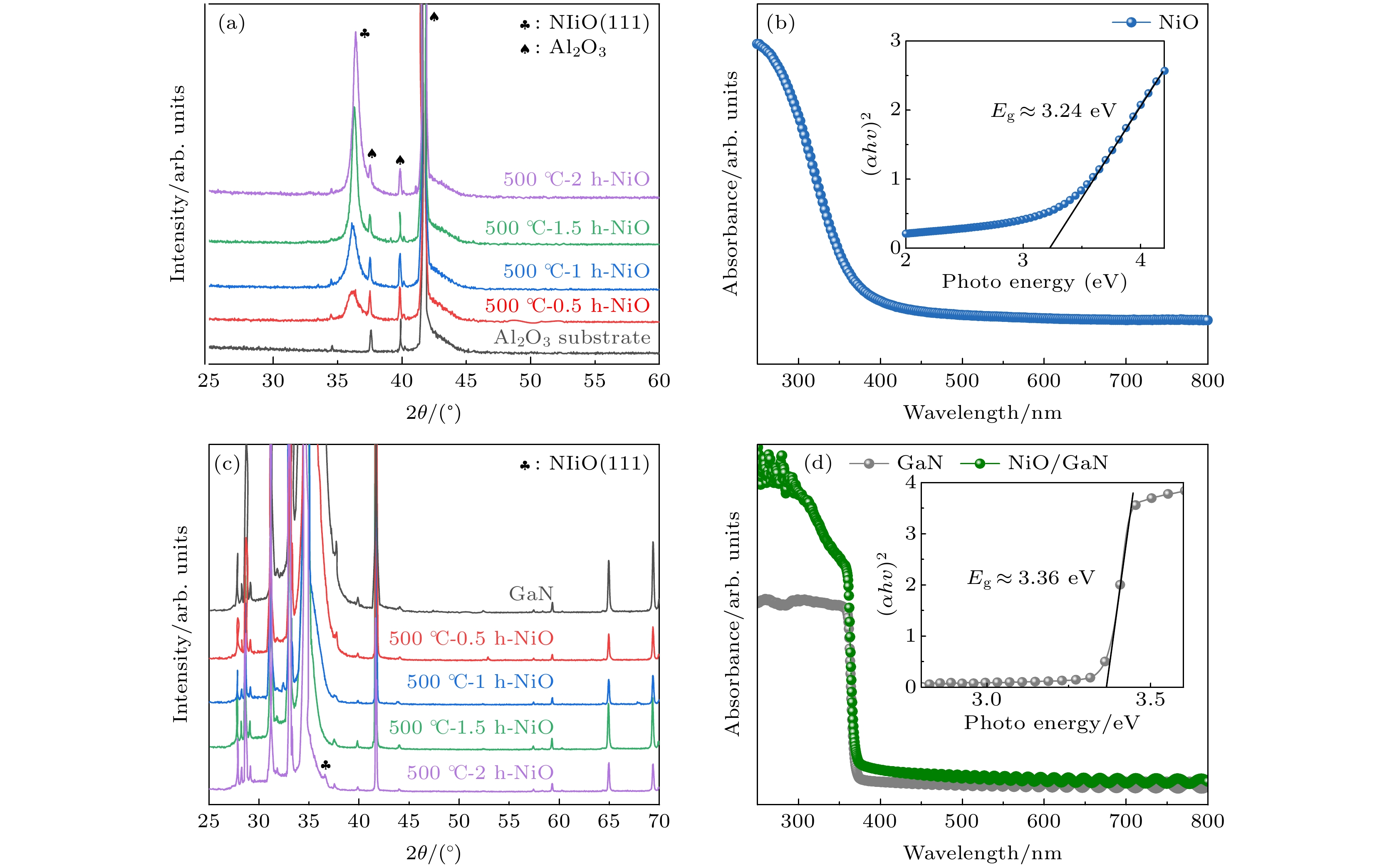
图 1 生长在蓝宝石衬底上的NiO薄膜的XRD图谱(a)和紫外-可见吸收图谱(b)以及NiO光学带隙(插图); 生长在GaN膜上的NiO薄膜的XRD图谱(c)和紫外-可见吸收图谱(d)以及GaN的光学带隙(插图)
Fig. 1. (a) XRD patterns and (b) UV-vis absorption spectra of the NiO film deposited on sapphire substrate (0001) plane. (panel (b) insert) Plots of (αhν)2 versus photon energy of the NiO film; (c) XRD patterns and (d) UV-vis absorption spectra of the NiO film deposited on GaN film. (panel (d) insert) Plots of (αhν)2 versus photon energy of the GaN film.
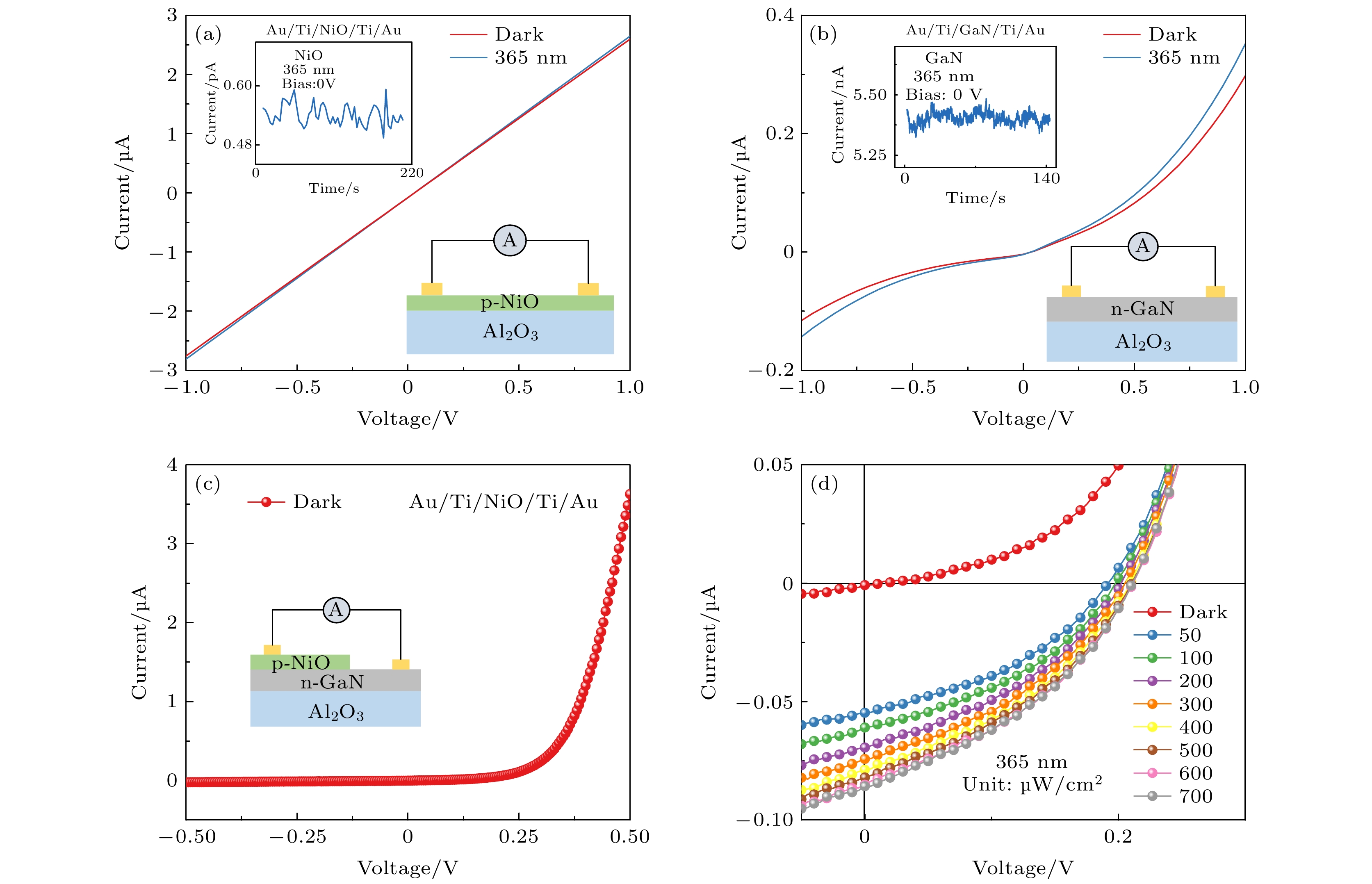
图 2 (a) 在365 nm光照下和黑暗中的NiO MSM结构的I -V曲线, 插图NiO MSM结构示意图和0 V下的I -T曲线; (b) 在365 nm光照下和黑暗中的GaN MSM结构的I -V曲线, 插图为GaN MSM结构示意图和0 V下的I -T曲线; (c) 黑暗中NiO/GaN p-n结的I -V特性, 插图为NiO/GaN p-n结器件结构示意图; (d) 不同强度的365 nm光照下NiO/GaN p-n结的I -V特性
Fig. 2. (a) I-V curves of the NiO MSM structure in dark and under 365 nm light illumination, (insert) diagram of the NiO MSM structure and I -T curve under zero bias; (b) I -V curves of the GaN MSM structure in dark and under 365 nm light illumination, (insert) diagram of the GaN MSM structure and I -T curve under zero bias; (c) I -V curve of the NiO/GaN p-n junction in dark, (insert) diagram of the device based on NiO/GaN p-n junction; (d) I -V curves of the NiO/GaN p-n junction under 365 nm light with various light intensities.
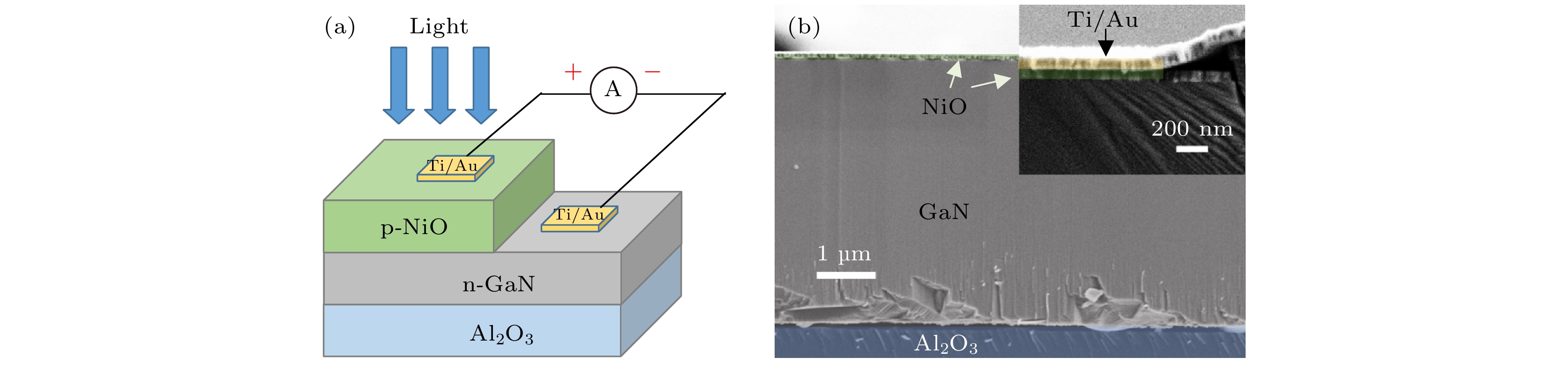
图 3 (a) 基于NiO/GaN p-n结的光电探测器结构示意图; (b) NiO/GaN p-n结的截面SEM图, 插图为镀有电极的p-n结截面SEM放大图
Fig. 3. (a) Schematic illustration of the fabricated prototype NiO/GaN p-n junction photodetector; (b) cross-sectional SEM image of the NiO/GaN p-n junction, where the insert is the enlargement cross-sectional SEM image of p-n junction with electrode plating.
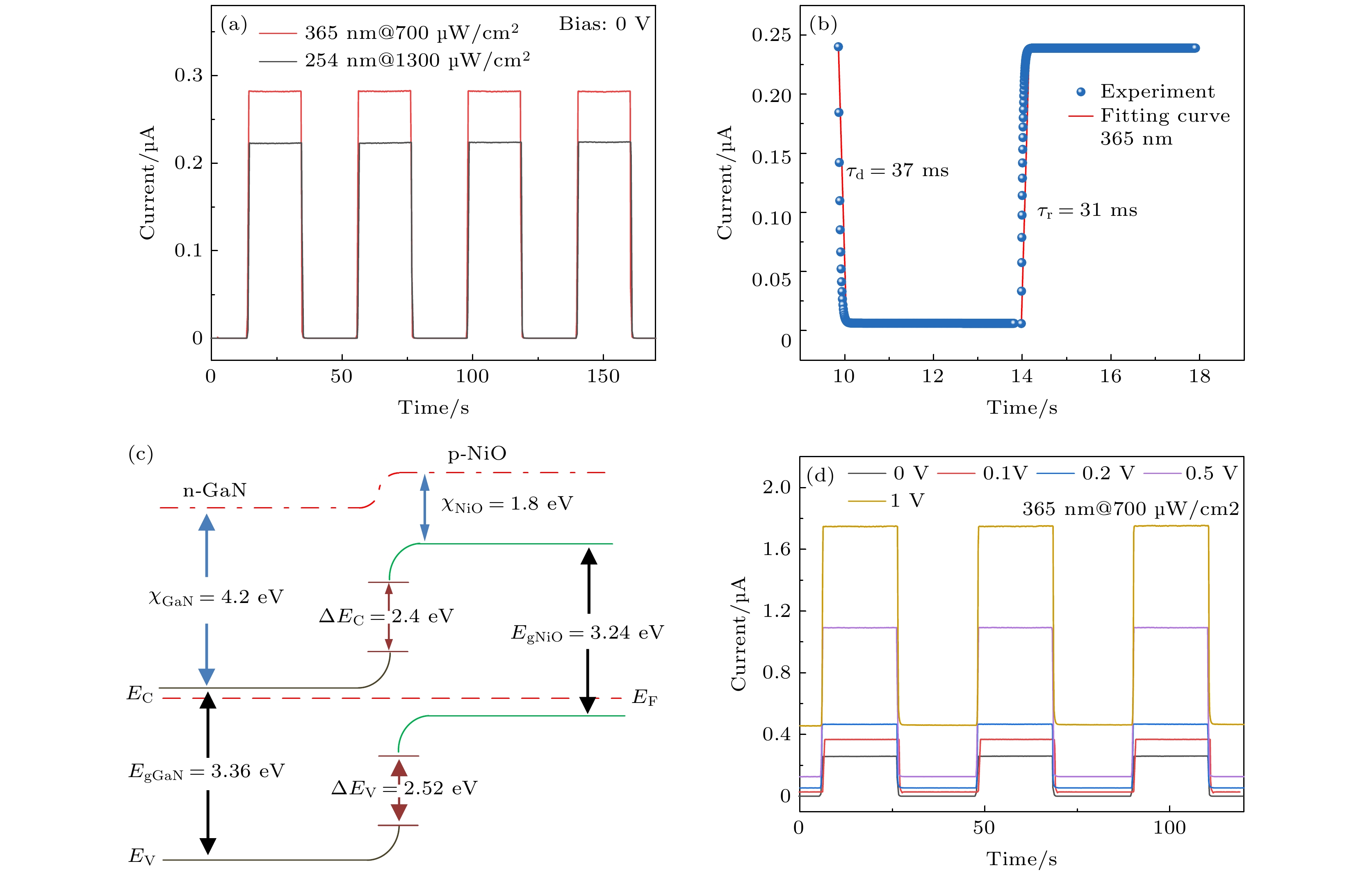
图 4 (a) 0 V电压下探测器对254和365 nm光照的I -T响应; (b) 对365 nm的光响应速度拟合; (c) NiO/GaN p-n结的能带图; (d) 不同偏压下探测器对365 nm光照的I -T响应
Fig. 4. (a) I -T curves of the photodetector under a zero bias at 254 and 365 nm illumination; (b) enlarged view of the rise/decay edges and the corresponding exponential fitting; (c) energy band diagrams of NiO/GaN p-n junction; (d) I -T curves of the photodetector under various biases with a 365 nm light illumination.
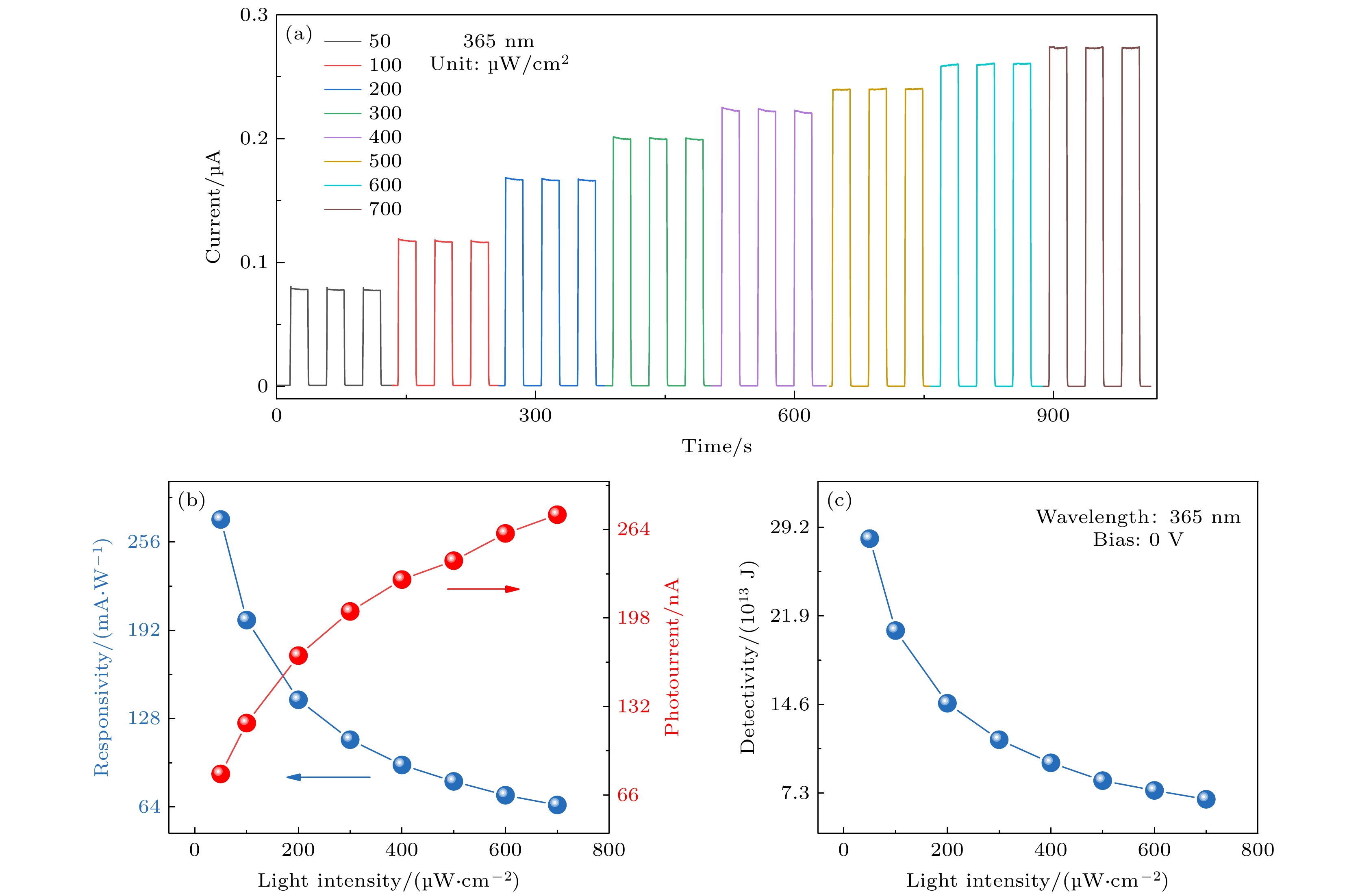
图 5 (a) 0 V偏压下探测器对不同光强的365 nm光照的I-T响应; (b) 光电流与响应度随光强的变化; (c) 探测率随光强的变化
Fig. 5. (a) Time-dependent photoresponse of the photodetector under zero bias and a 365 nm light with various light intensities; (b) photocurrent and responsivity as a function of light intensity; (c) detectivity as a function of light intensity.
表 1 基于GaN的自供电探测器件性能参数比较
Table 1. Self-powered device parameters comparison of photodetectors based on GaN from previous works and this work.
Photodetector Wavelength Responsivity/(mA·W–1) Detectivity/Jones Rise/Decay time/ms Ref. GaN/ZnO 350 nm 95.8 2.9 × 10¹² 730/50 [22] GaN/r-GO:Ag NPs 360 nm 266 2.62 × 10¹¹ 680/700 [23] GaN/NiO 365 nm 150 — — [20] GaN/Ga2O3 365 nm 54.49 — — [24] r-GO/GaN 350 nm 1.54 1.45 × 10¹¹ 60/267 [25] ZnO nanoarrays/CdS/GaN 300 nm 176 2.5 × 10¹² 350 [26] NiO/GaN 365 nm 272.3 2.83 × 10¹⁴ 31/37 This work  下载: 导出CSV
-
[1] Guo D, Chen K, Wang S, Wu F, Liu A, Li C, Li P, Tan C, Tang W 2020 Phys.Rev. Appl. 13 024051
Google Scholar
[2] 郭道友, 李培刚, 陈政委, 吴真平, 唐为华 2019 物理学报 68 078501
Google Scholar
Guo D Y, Li P G, Chen Z W, Wu Z P, Tang W H 2019 Acta Phys. Sin. 68 078501
Google Scholar
[3] Wu C, He C, Guo D, Zhang F, Li P, Wang S, Liu A, Wu F, Tang W 2020 Mater. Today Phys. 12 100193
Google Scholar
[4] Guo D, Guo Q, Chen Z, Wu Z, Li P, Tang W 2019 Materials Today Physics 11 100157
Google Scholar
[5] Strite S, Morkoç H 1992 J. Vac. Sci. Technol., B 10 1237
Google Scholar
[6] Li J, Xi X, Lin S, Ma Z, Li X, Zhao L 2020 ACS Appl. Mater. Interfaces 12 11965
Google Scholar
[7] Wang W, Zheng Y, Li X, Li Y, Huang L, Li G 2018 J. Mater. Chem. C 6 3417
Google Scholar
[8] Lee J H, Lee W W, Yang D W, Chang W J, Kwon S S, Park W I 2018 ACS Appl. Mater. Interfaces 10 14170
Google Scholar
[9] Xiao Y, Zhang W G, Tan Z T, Pan G B, Peng Z 2020 Chem. Phys. Lett. 739 136981
Google Scholar
[10] Zhuo R, Wang Y, Wu D, Lou Z, Shi Z, Xu T, Xu J, Tian Y, Li X 2018 J. Mater. Chem. C 6 299
Google Scholar
[11] Guo D, Su Y, Shi H, Li P, Zhao N, Ye J, Wang S, Liu A, Chen Z, Li C, Tang W 2018 ACS Nano 12 12827
Google Scholar
[12] De Vittorio M, Potì B, Todaro M, Frassanito M, Pomarico A, Passaseo A, Lomascolo M, Cingolani R 2004 Sens. Actuators, A 113 329
Google Scholar
[13] Guo X, Williamson T, Bohn P 2006 Solid State Commun. 140 159
Google Scholar
[14] Su L, Zhang Q, Wu T, Chen M, Su Y, Zhu Y, Xiang R, Gui X, Tang Z 2014 Appl. Phys. Lett. 105 072106
Google Scholar
[15] Zhu Y, Liu K, Ai Q, Hou Q, Chen X, Zhang Z, Xie X, Li B, Shen D 2020 J. Mater. Chem. C 8 2719
Google Scholar
[16] Wang Y, Wu C, Guo D, Li P, Wang S, Liu A, Li C, Wu F, Tang W 2020 ACS Appl. Electron. Mater. 2 2032
Google Scholar
[17] Koike K, Goto T, Nakamura S, Wada S, Fujii K 2018 MRS Commun. 8 480
Google Scholar
[18] Wang H, Zhang B L, Wu G G, Wu C, Shi Z F, Zhao Y, Wang J, Ma Y, Du G T, Dong X 2012 Chin. Phys. Lett. 29 107304
Google Scholar
[19] Yu N, Li H, Qi Y 2018 Opt. Mater. Express 9 26
Google Scholar
[20] Li L, Liu Z, Wang L, zhang B, Liu Y, Ao J P 2018 Mater. Sci. Semicond. Process. 76 61
Google Scholar
[21] Davis E, Mott N 1970 Philos. Mag. 22 903
Google Scholar
[22] Mishra M, Gundimeda A, Garg T, Dash A, Das S, Vandana, Gupta G 2019 Appl. Surf. Sci. 478 1081
Google Scholar
[23] Sarkar K, Hossain M, Devi P, Rao K D M, Kumar P 2019 Adv. Mater. Interfaces 6 1900923
Google Scholar
[24] Li P, Shi H, Chen K, Guo D, Cui W, Zhi Y, Wang S, Wu Z, Chen Z, Tang W 2017 J. Mater. Chem. C 5 10562
Google Scholar
[25] Prakash N, Singh M, Kumar G, Barvat A, Anand K, Pal P, Singh S P, Khanna S P 2016 Appl. Phys. Lett. 109 242102
Google Scholar
[26] Zhou H, Gui P, Yang L, Ye C, Xue M, Mei J, Song Z, Wang H 2017 New J. Chem. 41 4901
Google Scholar

 下载:
下载:
计量
- 文章访问数: 10677
- PDF下载量: 235
- 被引次数: 0
