-
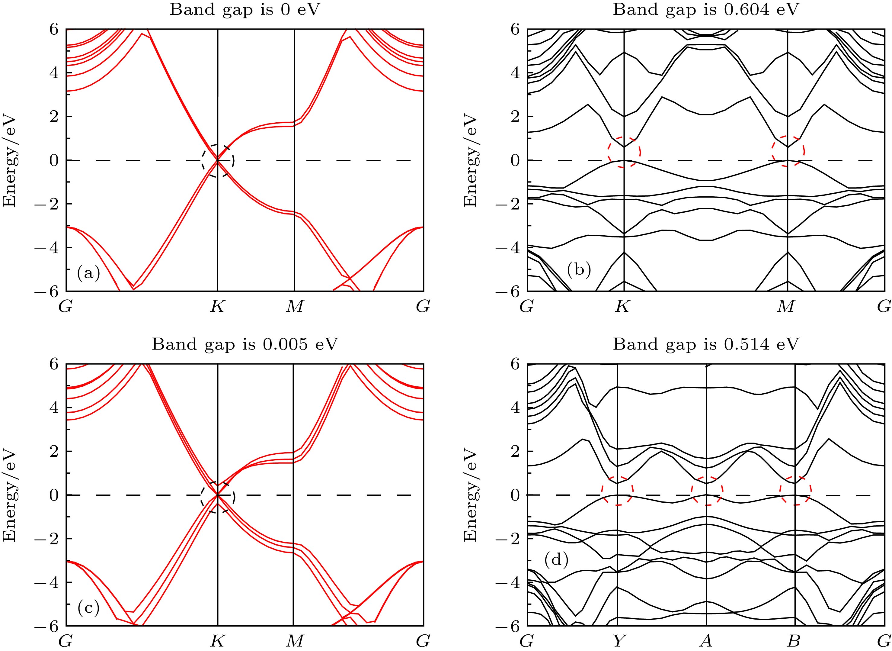
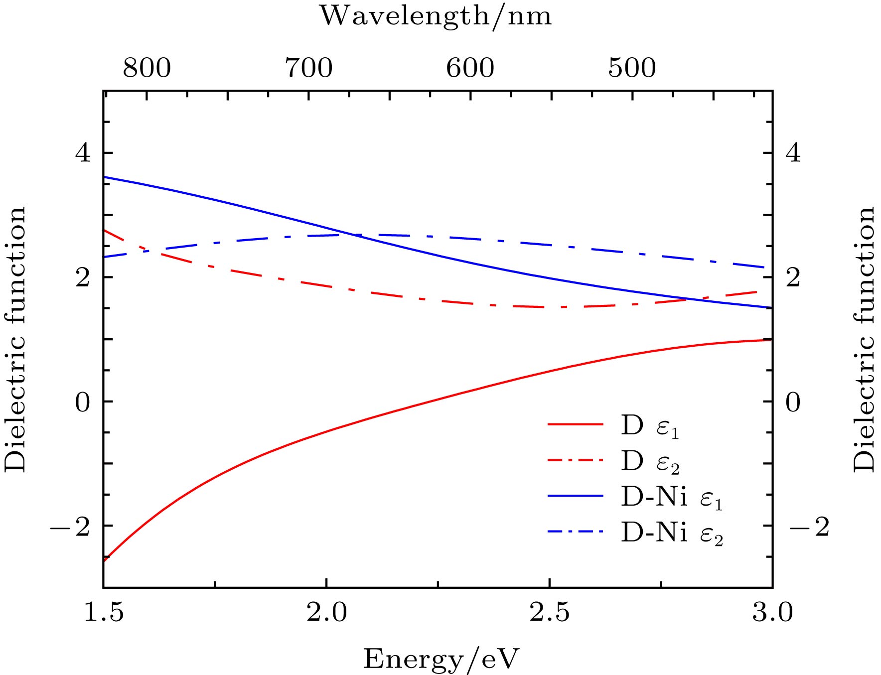
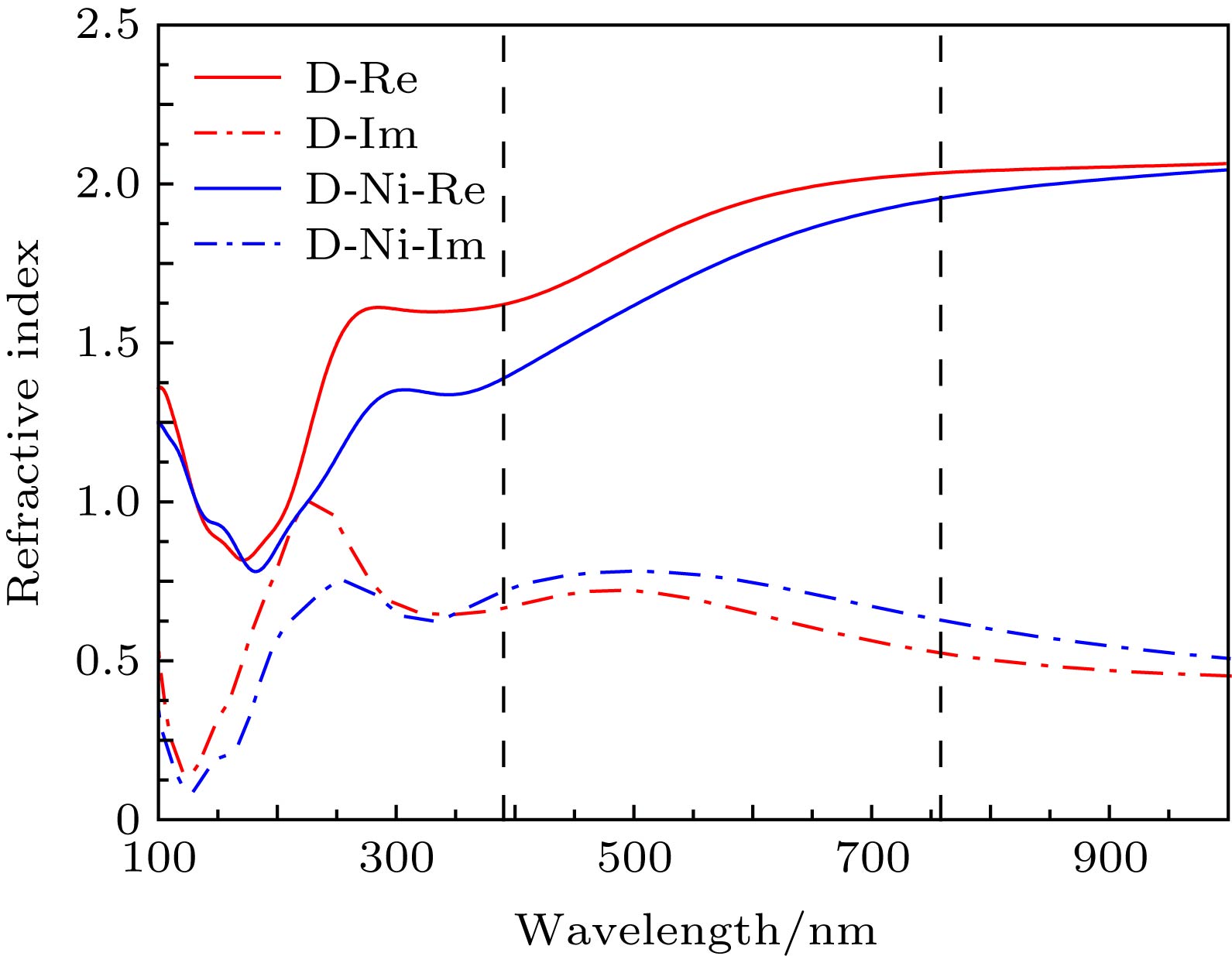
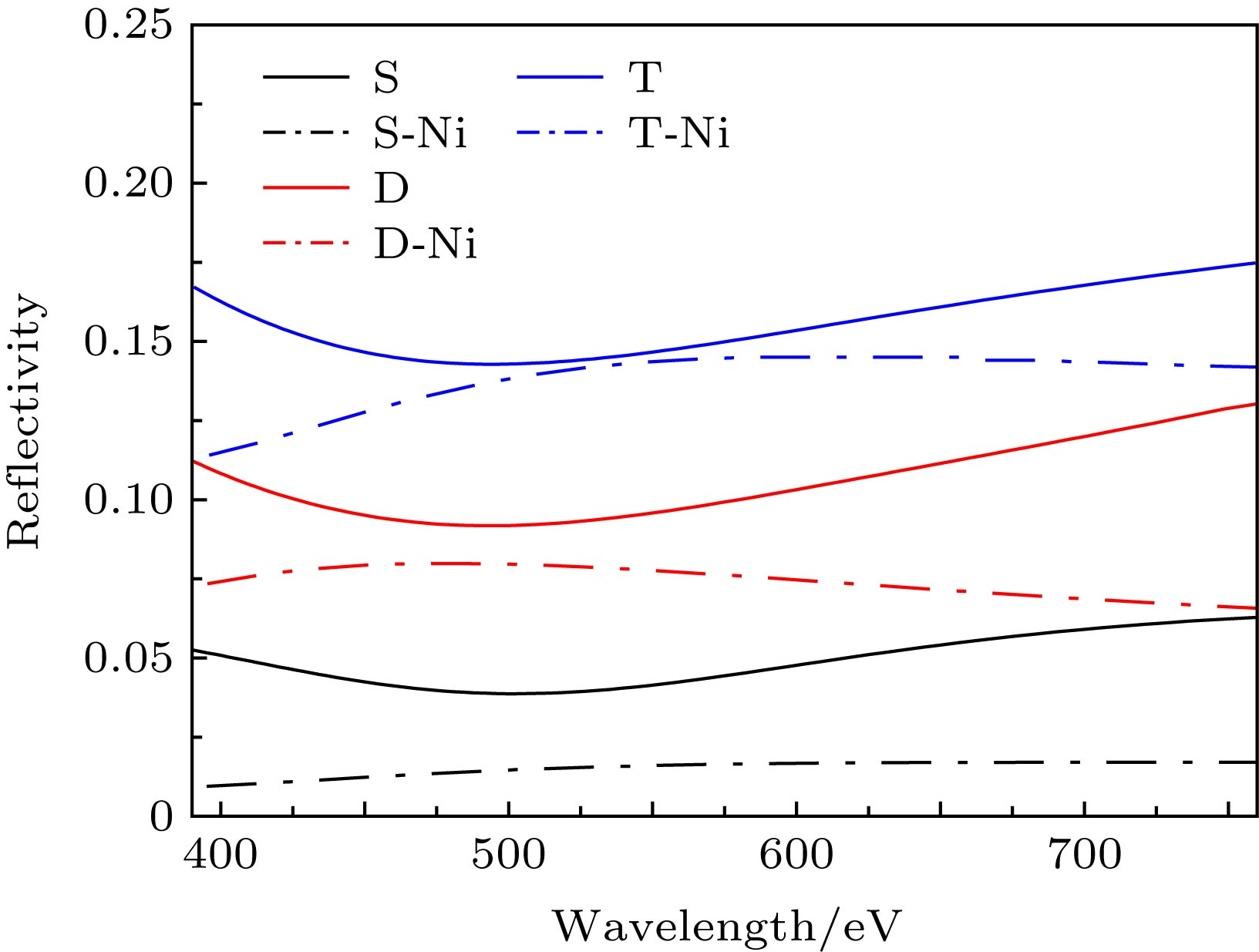
Graphene is an ideal two-dimensional crystal with the advantages of high conductivity, unique physical and chemical properties, and high specific surface area. Especially, because of its super excellent electronic properties, graphene may substitute the traditional semiconductor silicon material and carbon nanotube, thus creating a new nanoscale electronic device. In addition, multilayer graphene with ultra-wide spectral absorption characteristics and unique photoelectric properties is an ideal material for photovoltaic devices. However, the zero band gap and semi-metality of graphene both limit its application in space detectors such as the microelectronic industries and satellites. Opening and regulating the graphene band gap by physical methods has become one of the key means to further expand its applications. Research work has shown that the doping of elements can significantly change the electronic structure of graphene, thereby regulating the optical properties of graphene. In order to provide an insight into electronic properties of graphene and tune its electronic band structure and optical properties effectively, electronic and optical properties of Ni-doped multi-layer graphene are studied and a number of interesting results are obtained. The calculation are carried out by the CASTEP tool in Materials Studio software based on the first-principles of ultrasoft pseudopotential of density functional theory. The models of three typical doping positions relative to carbon atoms are constructed. After structural optimization, it is obtained that " above the center of two carbon atoms” is the most stable doping structure. By using the method of local density approximation, the band structure, density of states, dielectric constant, reflectivity and refractive index of the models are calculated. The results show that an enhanced energy band gap can be achieved after nickel-doping, and reach up to 0.604 eV. Besides, peaked phenomenon of density of states at Femi level can be observed, which is accomplished by enhancing the plasma energy. Furthermore, the calculations show that the imaginary part of permittivity and refractive index increase after nickel-doping, suggesting that the optical absorbing performance is improved. All these results provide theoretical guidance for further exploring the optical properties of graphene.
-
Keywords:
- graphene /
- first principle /
- Ni-doping /
- electronic structure /
- optical properties
[1] Geim A K N, Novoselov K S 2007 Nature Mat. 6 183
 Google Scholar
[2] Geim A K 2009 Science 324 1530
 Google Scholar
[3] Zhao M Z, Xu H, Xiong C X, Zheng M F, Zhang B H, Xie W K, Li H J 2018 Appl. Phys. Express 11 082002
 Google Scholar
[4] Zhang B H, Li H J, Xu H, Zhao M Z, Xiong C X, Liu C, Wu K 2019 Opt. Express 27 3598
 Google Scholar
[5] Yan Z L, Xiong X, Chen Y, Ouyang F P 2014 Superlattice Microst. 68 56
 Google Scholar
[6] 褚颖, 刘娟, 方庆, 蒋利军 2009 电池 39 220
 Google Scholar
Zhu Y, Liu J, Fang Q, Jiang L J 2009 The Battery 39 220
 Google Scholar
[7] 琚成, 贾芸芳 2014 太赫兹科学与电子信息学报 12 325
 Google Scholar
Ju C, Jia Y F 2014 Inf. Elect. Eng. 12 325
 Google Scholar
[8] Liu Y P, Xia Q L, He J, Liu Z W 2017 Nanoscale Res. Lett. 12 93
 Google Scholar
[9] 陈英良, 冯小波, 侯德东 2013 物理学报 62 187301
 Google Scholar
Chen Y L, Feng X B, Hou D D 2013 Acta Phys. Sin. 62 187301
 Google Scholar
[10] Schedin F, Geim A K, Morozov S V, Hill E W, Blake P, Katsnelson M L, Novoselov K S 2007 Nature Mater. 6 652
 Google Scholar
[11] Reddy A L M, Srivastava A, Gowda S R, Gullapalli H, Dubey M, Ajayan P M 2010 ACS Nano 4 6337
 Google Scholar
[12] Denis P A, Faccio R, Mombru A W 2009 ChemPhysChem 10 715
 Google Scholar
[13] Chi M, Zhao Y P 2009 Comput. Mater. Sci. 46 1085
 Google Scholar
[14] Endo M, Hayashi T, Hong S H, Enoki T, Dresselhaus M S 2001 J. Appl. Phys. 90 5670
 Google Scholar
[15] Jiang Q G, Ao Z M, Jiang Q 2013 Phys. Chem. Chem. Phys. 15 10859
 Google Scholar
[16] Rafique M, Shuai Y, Hussain N 2018 Physica E 95 94
 Google Scholar
[17] Luo G F, Wang L, Li H, Qin R, Zhou J, Li L Z, Gao Z X, Mei W N, Lu J, Nagase S 2011 J. Phys. Chem. C 115 24463
 Google Scholar
[18] 杨绍斌, 李思南, 唐树伟, 沈丁, 孙闻, 董伟 2016 原子与分子物理学报 33 1093
 Google Scholar
Yang S B, Li S N, Tang S W, Shen D, Sun W, Dong W 2016 J. At. Mol. Phys. 33 1093
 Google Scholar
[19] Nakada K, Ishii A 2011 Solid State Commun. 151 13
 Google Scholar
[20] Cui L L, Li X M, Cao C, Long M Q, Yang B C 2014 J. Appl. Phys. 116 033701
 Google Scholar
[21] Hu S Y, Liang C H, Tiong K K, Huang Y S 2007 J. Alloys Compd. 442 249
 Google Scholar
[22] Li S, Ahuja R, Barsoum M W, Jena P, Johansson B 2008 Appl. Phys. Lett. 92 221907
 Google Scholar
[23] Xu H, Zhao M Z, Zheng M F, Xiong C X, Zhang B H, Peng Y Y, Li H J 2019 J. Phys. D: Appl. Phys. 52 025104
[24] Jiao Z Y, Ma S H, Yang J F 2011 Solid State Sci. 13 331
[25] Lin X L, Niu C P, Pan F C, Chen H M, Wang X M 2017 Physica B 521 371
 Google Scholar
[26] 禹忠, 党忠, 柯熙政, 崔真 2016 物理学报 65 248103
 Google Scholar
Yu Z, Dang Z, Ke X Z, Cui Z 2016 Acta Phys. Sin. 65 248103
 Google Scholar
-
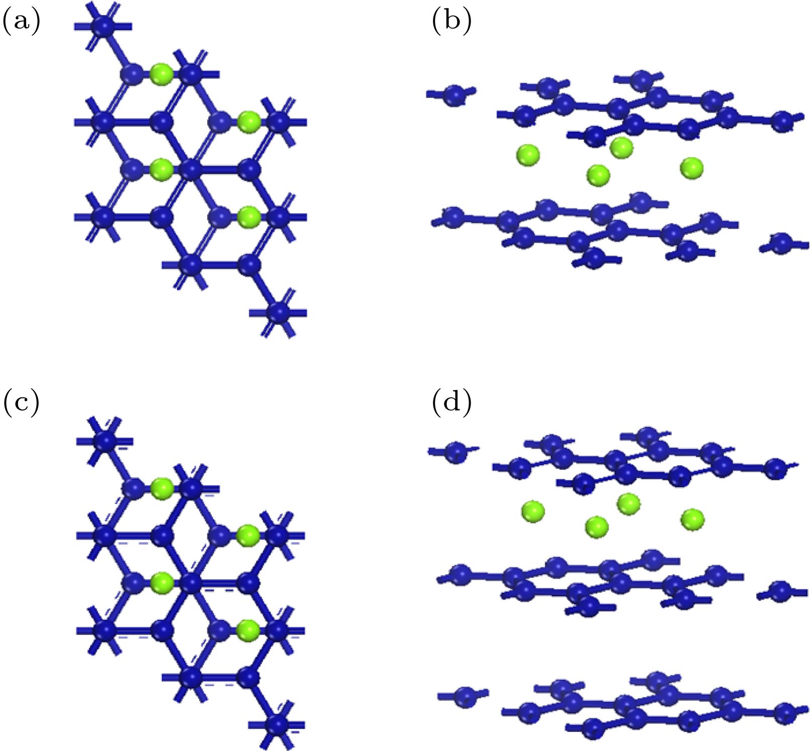
图 1 镍原子掺杂的双层石墨烯的(a)俯视图和(b)侧视图; 镍原子掺杂的三层石墨烯的(c)俯视图和(d)侧视图(蓝色代表石墨烯, 绿色代表镍原子)
Fig. 1. (a) Top view and (b) side view of bilayer graphene cell (marked as blue) doped with nickel (marked as green); (c) top view and (d) side view of trilayer graphene cell (marked as blue) doped with nickel (marked as green).
-
[1] Geim A K N, Novoselov K S 2007 Nature Mat. 6 183
 Google Scholar
[2] Geim A K 2009 Science 324 1530
 Google Scholar
[3] Zhao M Z, Xu H, Xiong C X, Zheng M F, Zhang B H, Xie W K, Li H J 2018 Appl. Phys. Express 11 082002
 Google Scholar
[4] Zhang B H, Li H J, Xu H, Zhao M Z, Xiong C X, Liu C, Wu K 2019 Opt. Express 27 3598
 Google Scholar
[5] Yan Z L, Xiong X, Chen Y, Ouyang F P 2014 Superlattice Microst. 68 56
 Google Scholar
[6] 褚颖, 刘娟, 方庆, 蒋利军 2009 电池 39 220
 Google Scholar
Zhu Y, Liu J, Fang Q, Jiang L J 2009 The Battery 39 220
 Google Scholar
[7] 琚成, 贾芸芳 2014 太赫兹科学与电子信息学报 12 325
 Google Scholar
Ju C, Jia Y F 2014 Inf. Elect. Eng. 12 325
 Google Scholar
[8] Liu Y P, Xia Q L, He J, Liu Z W 2017 Nanoscale Res. Lett. 12 93
 Google Scholar
[9] 陈英良, 冯小波, 侯德东 2013 物理学报 62 187301
 Google Scholar
Chen Y L, Feng X B, Hou D D 2013 Acta Phys. Sin. 62 187301
 Google Scholar
[10] Schedin F, Geim A K, Morozov S V, Hill E W, Blake P, Katsnelson M L, Novoselov K S 2007 Nature Mater. 6 652
 Google Scholar
[11] Reddy A L M, Srivastava A, Gowda S R, Gullapalli H, Dubey M, Ajayan P M 2010 ACS Nano 4 6337
 Google Scholar
[12] Denis P A, Faccio R, Mombru A W 2009 ChemPhysChem 10 715
 Google Scholar
[13] Chi M, Zhao Y P 2009 Comput. Mater. Sci. 46 1085
 Google Scholar
[14] Endo M, Hayashi T, Hong S H, Enoki T, Dresselhaus M S 2001 J. Appl. Phys. 90 5670
 Google Scholar
[15] Jiang Q G, Ao Z M, Jiang Q 2013 Phys. Chem. Chem. Phys. 15 10859
 Google Scholar
[16] Rafique M, Shuai Y, Hussain N 2018 Physica E 95 94
 Google Scholar
[17] Luo G F, Wang L, Li H, Qin R, Zhou J, Li L Z, Gao Z X, Mei W N, Lu J, Nagase S 2011 J. Phys. Chem. C 115 24463
 Google Scholar
[18] 杨绍斌, 李思南, 唐树伟, 沈丁, 孙闻, 董伟 2016 原子与分子物理学报 33 1093
 Google Scholar
Yang S B, Li S N, Tang S W, Shen D, Sun W, Dong W 2016 J. At. Mol. Phys. 33 1093
 Google Scholar
[19] Nakada K, Ishii A 2011 Solid State Commun. 151 13
 Google Scholar
[20] Cui L L, Li X M, Cao C, Long M Q, Yang B C 2014 J. Appl. Phys. 116 033701
 Google Scholar
[21] Hu S Y, Liang C H, Tiong K K, Huang Y S 2007 J. Alloys Compd. 442 249
 Google Scholar
[22] Li S, Ahuja R, Barsoum M W, Jena P, Johansson B 2008 Appl. Phys. Lett. 92 221907
 Google Scholar
[23] Xu H, Zhao M Z, Zheng M F, Xiong C X, Zhang B H, Peng Y Y, Li H J 2019 J. Phys. D: Appl. Phys. 52 025104
[24] Jiao Z Y, Ma S H, Yang J F 2011 Solid State Sci. 13 331
[25] Lin X L, Niu C P, Pan F C, Chen H M, Wang X M 2017 Physica B 521 371
 Google Scholar
[26] 禹忠, 党忠, 柯熙政, 崔真 2016 物理学报 65 248103
 Google Scholar
Yu Z, Dang Z, Ke X Z, Cui Z 2016 Acta Phys. Sin. 65 248103
 Google Scholar
计量
- 文章访问数: 18727
- PDF下载量: 321
- 被引次数: 0


 下载:
下载:
