-
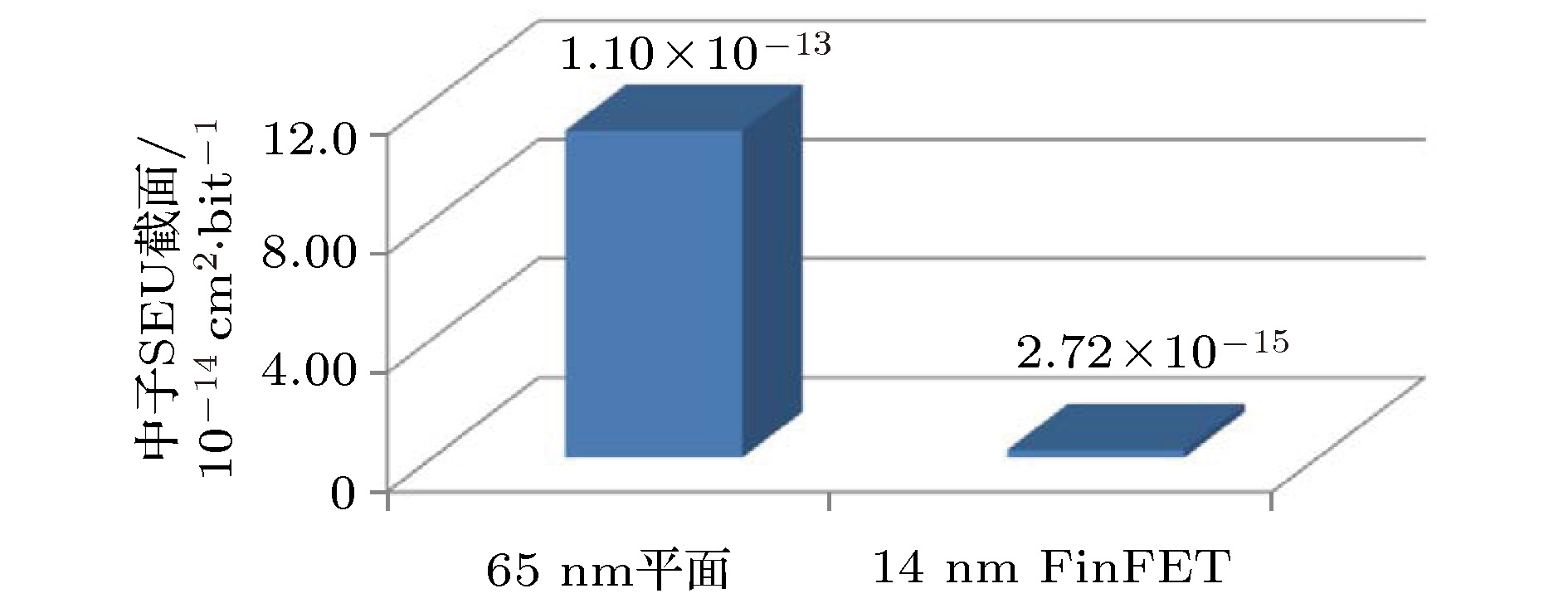
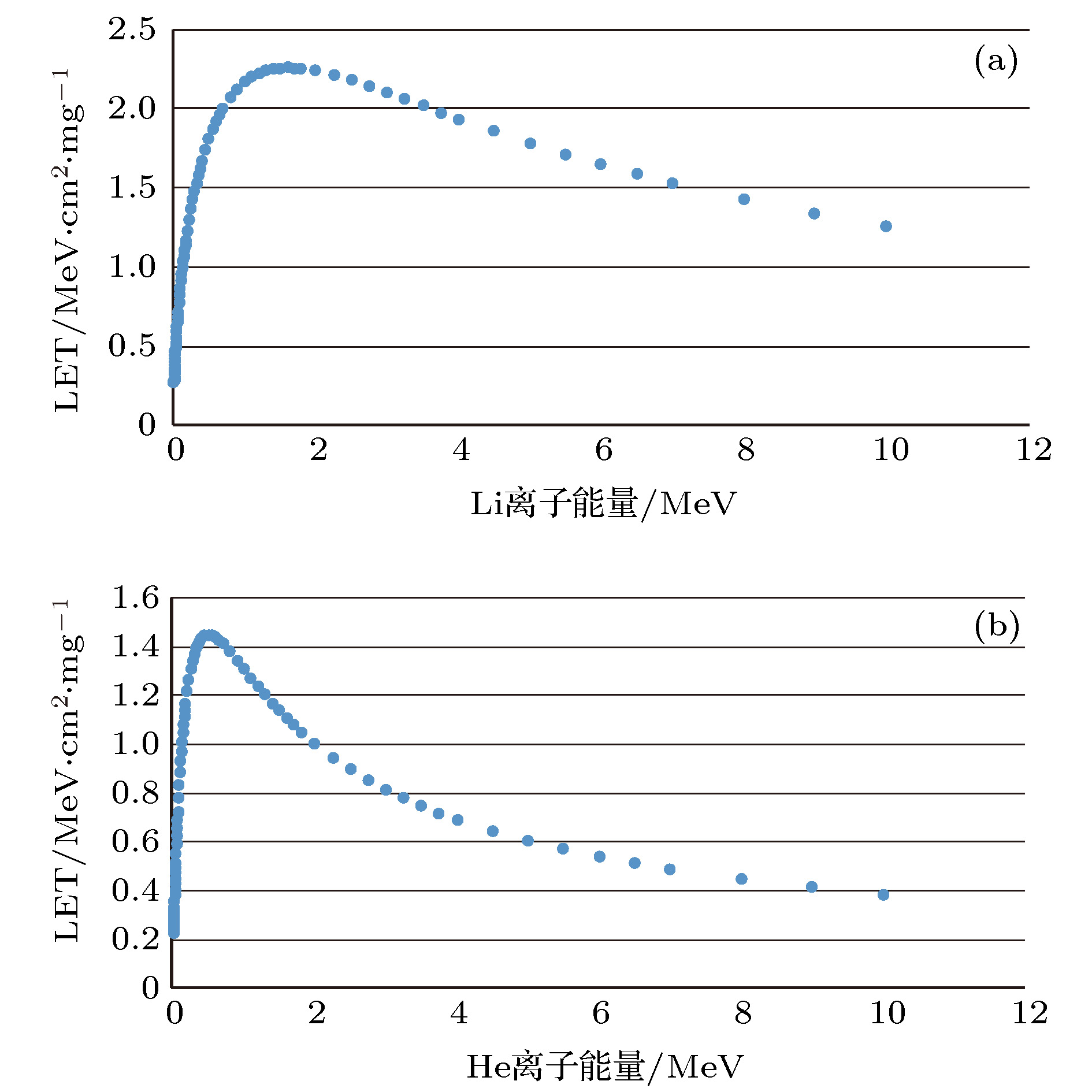
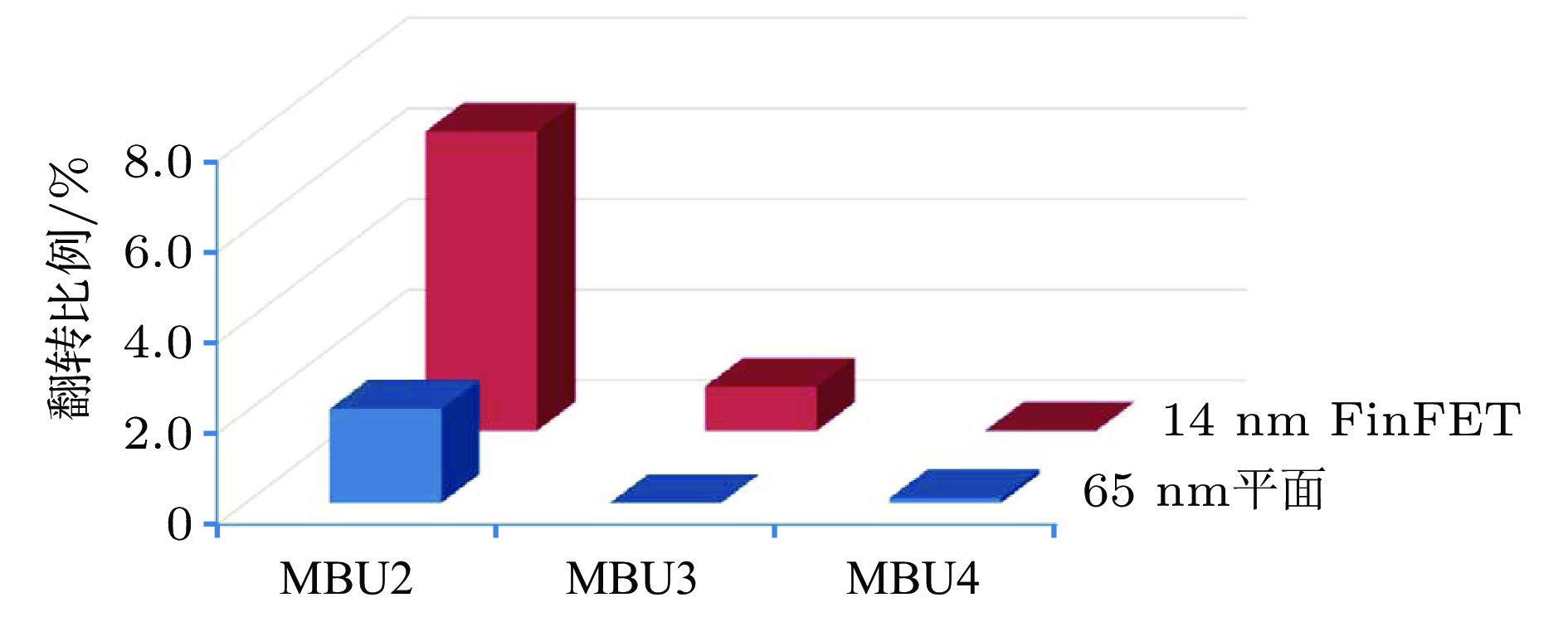
使用中国散裂中子源提供的宽能谱中子束流, 开展14 nm FinFET工艺和65 nm平面工艺静态随机存取存储器中子单粒子翻转对比研究, 发现相比于65 nm器件, 14 nm FinFET器件的大气中子单粒子翻转截面下降至约1/40, 而多位翻转比例从2.2%增大至7.6%, 源于14 nm FinFET器件灵敏区尺寸(80 nm × 30 nm × 45 nm)、间距和临界电荷(0.05 fC)的减小. 不同于65 nm器件对热中子免疫的现象, 14 nm FinFET器件中M0附近10B元素的使用导致其表现出一定的热中子敏感性. 进一步的中子输运仿真结果表明, 高能中子在器件灵敏区中产生的大量的射程长、LET值大的高Z二次粒子是多位翻转的产生诱因, 而单粒子翻转主要来自于p, He, Si等轻离子的贡献.
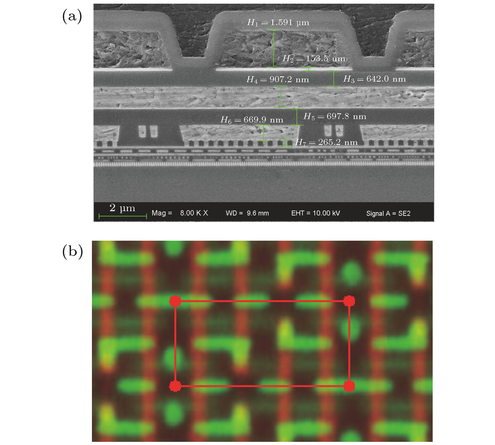
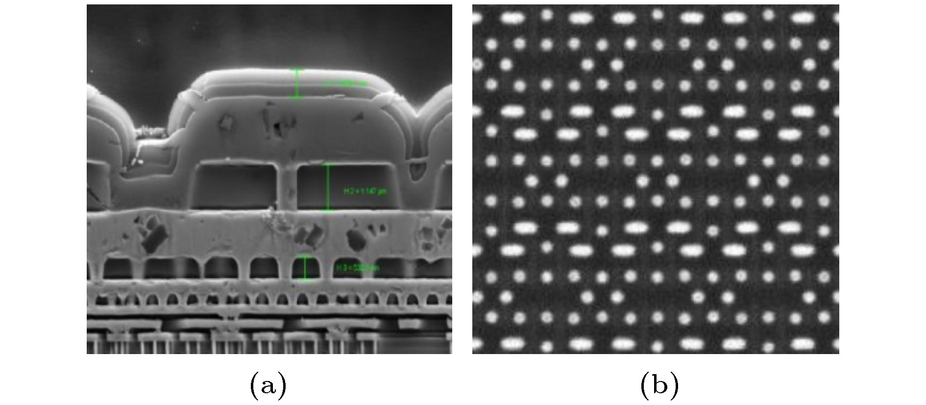
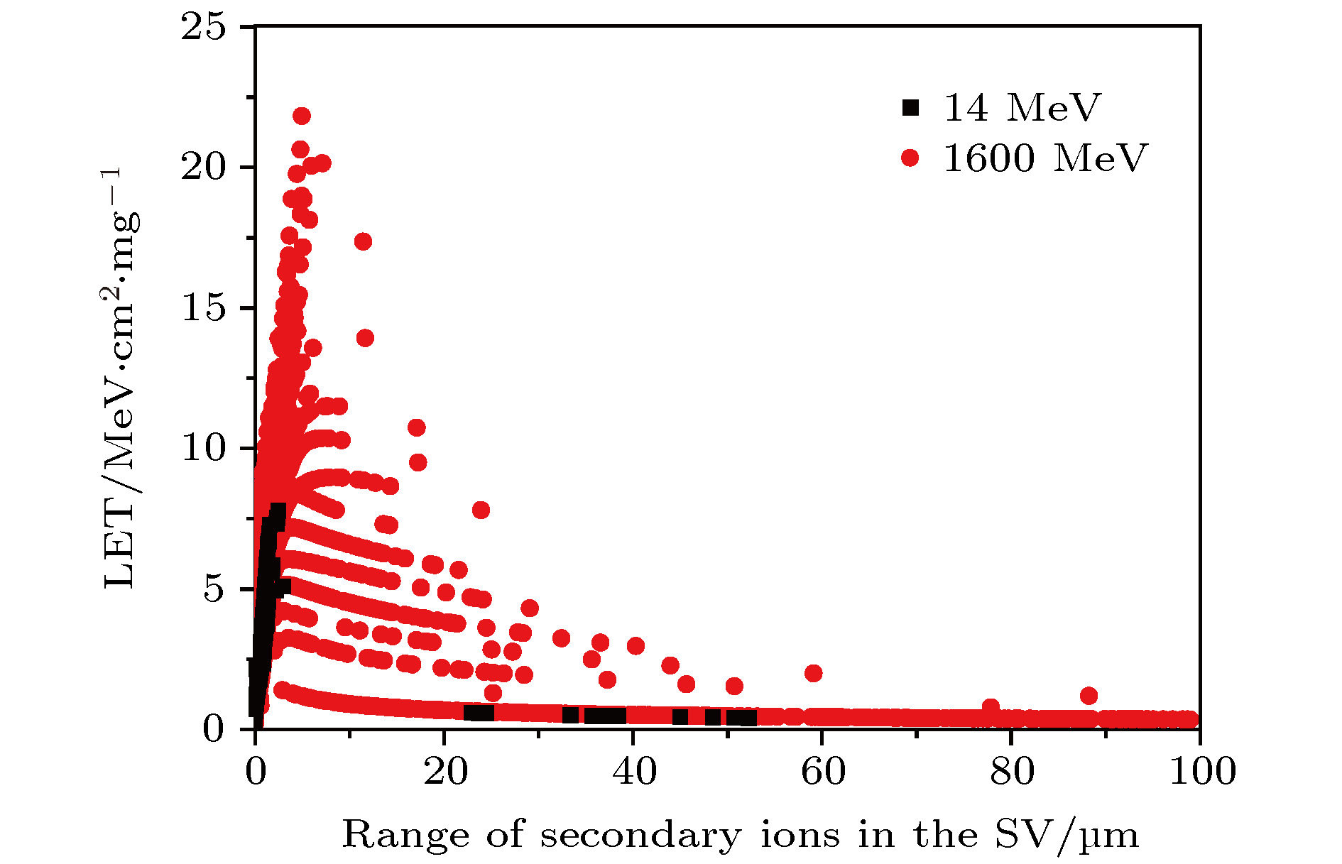
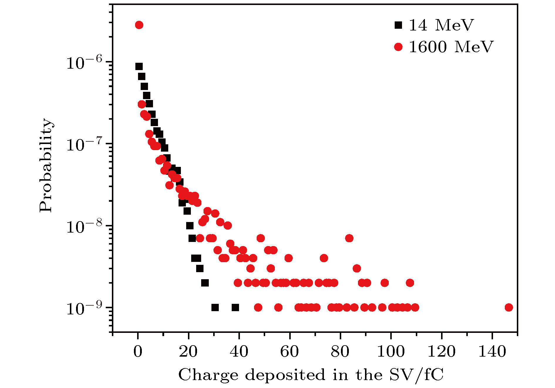
Based on the wide-spectrum neutron beam (covering thermal neutrons and E > 10 MeV neutrons, with maximum energy of 1.6 GeV) provided by the China Spallation Neutron Source (CSNS), this paper focuses on the single event effect study of 14 nm FinFET large-capacity SRAM and 65 nm planar process SRAM device, using combined techniques of irradiation experiment, reverse analysis, and Monte-Carlo neutron transport simulation. The aim is to reveal the effect of integrated circuit process changing on the sensitivity of neutron induced single-bit and multiple-bit upsets (MBU), and to analyze the inner mechanisms, including the distribution of secondary particles in the sensitive volume, the characteristics of deposited charges, etc. The results show that compared with the 65 nm device, single event upset (SEU) cross section of the 14 nm FinFET device, induced by E > 10 MeV neutrons, is reduced by about 40 times, while the MBU ratio increases from 2.2% to 7.6%, which is due to the reduction of sensitive volume size of the 14 nm FinFET device (80 nm × 30 nm × 45 nm), pitch, and critical charge (0.05 fC). The main forms of MBU are double-bit upset, triple-bit upset and quadruple-bit upset. Unlike the phenomenon that the 65 nm device is immune to thermal neutrons, the use of the 10B element near M0 in the 14 nm FinFET device causes it to present the thermal neutron sensitivity to a certain extent. The SEU cross section induced by thermal neutrons is about 4.8 times smaller than that induced by E > 10 MeV neutrons. Based on the device cross-section and memory area images obtained from the reverse analysis, a device model is established and neutron transport simulation based on Geant4 toolkit is carried out. The E > 10 MeV neutrons result in abundant secondary particle distribution in the sensitive volume of the device, covering n, p into even W. The neutron energy and presence or absence of the W plug near the sensitive volume have an importantinfluence on the type and probability of secondary particles in the sensitive volume. The analysis and calculations show that a large number of high-Z secondary particles with long range and large LET values generated by high-energy neutrons in the sensitive volume of the device are the inducement of MBU, and SEUs mainly result from the contribution of light ions such as p, He, and Si. -
Keywords:
- FinFET /
- neutron /
- single event upset /
- nuclear reaction
[1] Lu D D, Dunga M V, Lin C S, Niknejad A M, Hu C 2007 IEEE International Electron Devices Meeting Washington, DC, USA, December 10–12, 2007 p565
[2] Park T, Choi S, Lee D H, Yoo J R, Lee B C, Kim J Y, Lee C G, Chi K K, Hong S H, Hynn S J, Shin Y G, Han J N, Park I S, Chung U I, Moon J T, Yoon E, Lee J H 2003 Symposium on VLSI Technology Kyoto, Japan, June 10–12, 2003 p135
[3] Manoj C R, Meenakshi N, Dhanya V, Rao V R 2007 International Workshop on Physics of Semiconductor Devices Mumbai, India, December 16–20, 2007 p134
[4] Ma C, Li B, Zhang L, He J, Zhang X, Lin X, Chan M 2009 10th International Symposium on Quality Electronic Design San Jose, CA, USA, March 16–18, 2009 p7
[5] [6] Lei Z F, Zhang Z G, En Y F, Huang Y 2018 Chin. Phys. B 27 066105
 Google Scholar
[7] JESD89 A Measurement and Reporting of Alpha Particle and Terrestrial Cosmic Ray-Induced Soft Errors in Semiconductor Devices JEDEC standard, October 2006
[8] May T C, Woods M H 1979 IEEE Trans. Electron Dev. ED-26 2
[9] Autran J L, Munteanu D, Sauze S, Gasiot G, Roche P 2014 IEEE Radiation Effects Data Workshop (REDW) Paris, France, July 14–18, 2014 p1
[10] Auden E C, Quinn H M, Wender S A, O’Donnell J M, Lisowski P W, George J S, Xu N, Black D A, Black J D 2019 IEEE Trans. Nucl. Sci. Early Access 1
[11] Weulersse C, Houssany S, Guibbaud N, Segura-Ruiz J, Beaucour J, Miller F, Mazurek M 2018 IEEE Trans. Nucl. Sci. 65 1851
 Google Scholar
[12] Zhang H, Jiang H, Brockman J D, Assis T R, Fan X, Bhuva B L, Narasimham B, Wen S J, Wong R 2017 IEEE International Reliability Physics Symposium (IRPS) Monterey, CA, USA, April 2–6, 2017 p3 D-3.1
[13] Seifert N, Jahinuzzaman S, Velamala J, Ascazubi R, Patel N, Gill B, Basile J, Hicks J 2015 IEEE Trans. Nucl. Sci. 62 2570
 Google Scholar
[14] Fang Y, Oates A S 2011 IEEE Trans. Dev. Mater. Reliab. 11 551
 Google Scholar
[15] 王勋, 张凤祁, 陈伟, 郭晓强, 丁李利, 罗尹虹 2019 物理学报 68 052901
 Google Scholar
Wang X, Zhang F Q, Chen W, Guo X Q, Ding L L, Luo Y H 2019 Acta Phys. Sin. 68 052901
 Google Scholar
[16] Ziegler J F, Biersack J P, Littmark U 1985 The Stopping and Range of Ions in Solids (New York: Pergamon Press)
[17] SRIM & TRIM, Ziegler J F http://www.srim.org/ [2019-7-11]
[18] Zhang Z G, Lei Z F, En Y F, Liu J 2016 Radiation Effects on Components & Systems Conference (RADECS) Bremen, Germany, September 19–23, 2016 Paper H14
[19] Sierawski B D, Mendenhall M H, Reed R A, Clemens M A, Weller R A, Schrimpf R D, Blackmore E W, Trinczek M, Hitti B, Pellish J A, Baumann R C, Wen S J, Wong R, Tam N 2010 IEEE Tran. Nucl. Sci. 57 3273
[20] Agostinelli S, Allison J, Amako K, et al. 2003 Nucl. Instrum. Meth. Phys. Res. A 506 250
 Google Scholar
[21] Zhang Z G, Liu J, Sun Y M, Hou M D, Tong T, Gu S, Liu T Q, Geng C, Xi K, Yao H J, Luo J, Duan J L, Mo D, Su H, Lei Z F, En Y F, Huang Y 2014 10th International Conference on Reliability, Maintainability and Safety (ICRMS) Guangzhou, China, August 6–8, 2014 p114
-
表 1 被测器件参数
Table 1. Parameters of devices under test.
编号 SRAM工艺 型号 容量 供电电压(core)/V 封装形式 1# 65 nm平面 CY7 C1663 KV18 8 Mb × 18 1.8 BGA, 非倒装 2# 14 nm FinFET — 8 Mb × 16 0.8 BGA, 倒装 表 2 14 nm FinFET SRAM和65 nm SRAM的存储单元尺寸和灵敏区参数
Table 2. Memory cell size and SV parameters for the 14 nm FinFET SRAM and 65 nm SRAM devices.
-
[1] Lu D D, Dunga M V, Lin C S, Niknejad A M, Hu C 2007 IEEE International Electron Devices Meeting Washington, DC, USA, December 10–12, 2007 p565
[2] Park T, Choi S, Lee D H, Yoo J R, Lee B C, Kim J Y, Lee C G, Chi K K, Hong S H, Hynn S J, Shin Y G, Han J N, Park I S, Chung U I, Moon J T, Yoon E, Lee J H 2003 Symposium on VLSI Technology Kyoto, Japan, June 10–12, 2003 p135
[3] Manoj C R, Meenakshi N, Dhanya V, Rao V R 2007 International Workshop on Physics of Semiconductor Devices Mumbai, India, December 16–20, 2007 p134
[4] Ma C, Li B, Zhang L, He J, Zhang X, Lin X, Chan M 2009 10th International Symposium on Quality Electronic Design San Jose, CA, USA, March 16–18, 2009 p7
[5] [6] Lei Z F, Zhang Z G, En Y F, Huang Y 2018 Chin. Phys. B 27 066105
 Google Scholar
[7] JESD89 A Measurement and Reporting of Alpha Particle and Terrestrial Cosmic Ray-Induced Soft Errors in Semiconductor Devices JEDEC standard, October 2006
[8] May T C, Woods M H 1979 IEEE Trans. Electron Dev. ED-26 2
[9] Autran J L, Munteanu D, Sauze S, Gasiot G, Roche P 2014 IEEE Radiation Effects Data Workshop (REDW) Paris, France, July 14–18, 2014 p1
[10] Auden E C, Quinn H M, Wender S A, O’Donnell J M, Lisowski P W, George J S, Xu N, Black D A, Black J D 2019 IEEE Trans. Nucl. Sci. Early Access 1
[11] Weulersse C, Houssany S, Guibbaud N, Segura-Ruiz J, Beaucour J, Miller F, Mazurek M 2018 IEEE Trans. Nucl. Sci. 65 1851
 Google Scholar
[12] Zhang H, Jiang H, Brockman J D, Assis T R, Fan X, Bhuva B L, Narasimham B, Wen S J, Wong R 2017 IEEE International Reliability Physics Symposium (IRPS) Monterey, CA, USA, April 2–6, 2017 p3 D-3.1
[13] Seifert N, Jahinuzzaman S, Velamala J, Ascazubi R, Patel N, Gill B, Basile J, Hicks J 2015 IEEE Trans. Nucl. Sci. 62 2570
 Google Scholar
[14] Fang Y, Oates A S 2011 IEEE Trans. Dev. Mater. Reliab. 11 551
 Google Scholar
[15] 王勋, 张凤祁, 陈伟, 郭晓强, 丁李利, 罗尹虹 2019 物理学报 68 052901
 Google Scholar
Wang X, Zhang F Q, Chen W, Guo X Q, Ding L L, Luo Y H 2019 Acta Phys. Sin. 68 052901
 Google Scholar
[16] Ziegler J F, Biersack J P, Littmark U 1985 The Stopping and Range of Ions in Solids (New York: Pergamon Press)
[17] SRIM & TRIM, Ziegler J F http://www.srim.org/ [2019-7-11]
[18] Zhang Z G, Lei Z F, En Y F, Liu J 2016 Radiation Effects on Components & Systems Conference (RADECS) Bremen, Germany, September 19–23, 2016 Paper H14
[19] Sierawski B D, Mendenhall M H, Reed R A, Clemens M A, Weller R A, Schrimpf R D, Blackmore E W, Trinczek M, Hitti B, Pellish J A, Baumann R C, Wen S J, Wong R, Tam N 2010 IEEE Tran. Nucl. Sci. 57 3273
[20] Agostinelli S, Allison J, Amako K, et al. 2003 Nucl. Instrum. Meth. Phys. Res. A 506 250
 Google Scholar
[21] Zhang Z G, Liu J, Sun Y M, Hou M D, Tong T, Gu S, Liu T Q, Geng C, Xi K, Yao H J, Luo J, Duan J L, Mo D, Su H, Lei Z F, En Y F, Huang Y 2014 10th International Conference on Reliability, Maintainability and Safety (ICRMS) Guangzhou, China, August 6–8, 2014 p114
计量
- 文章访问数: 13745
- PDF下载量: 199
- 被引次数: 0


 下载:
下载:

