


-
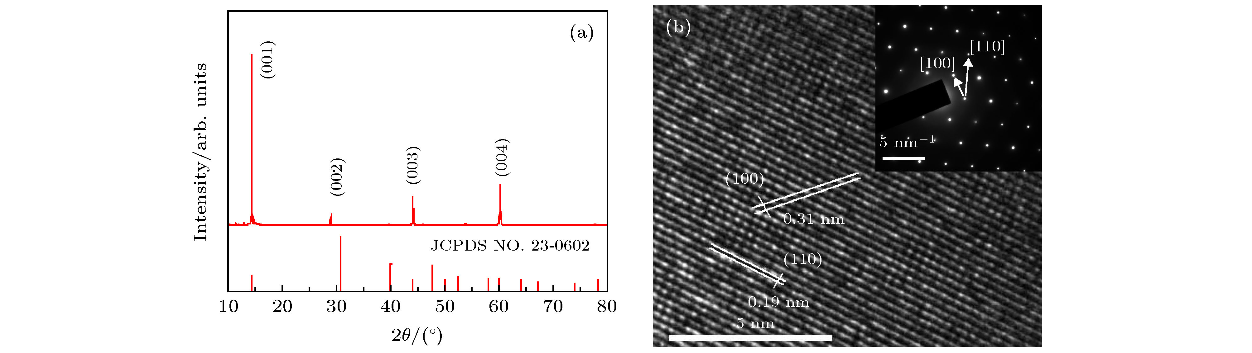
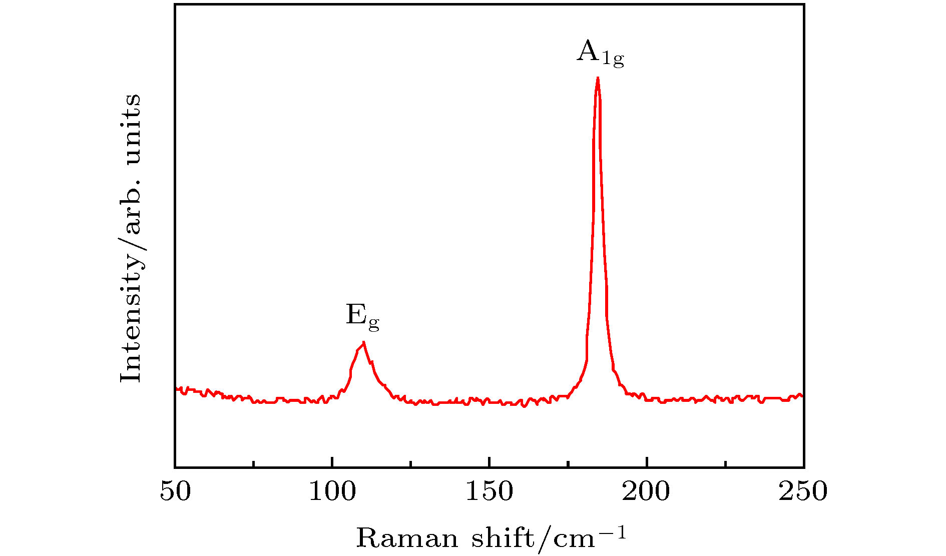
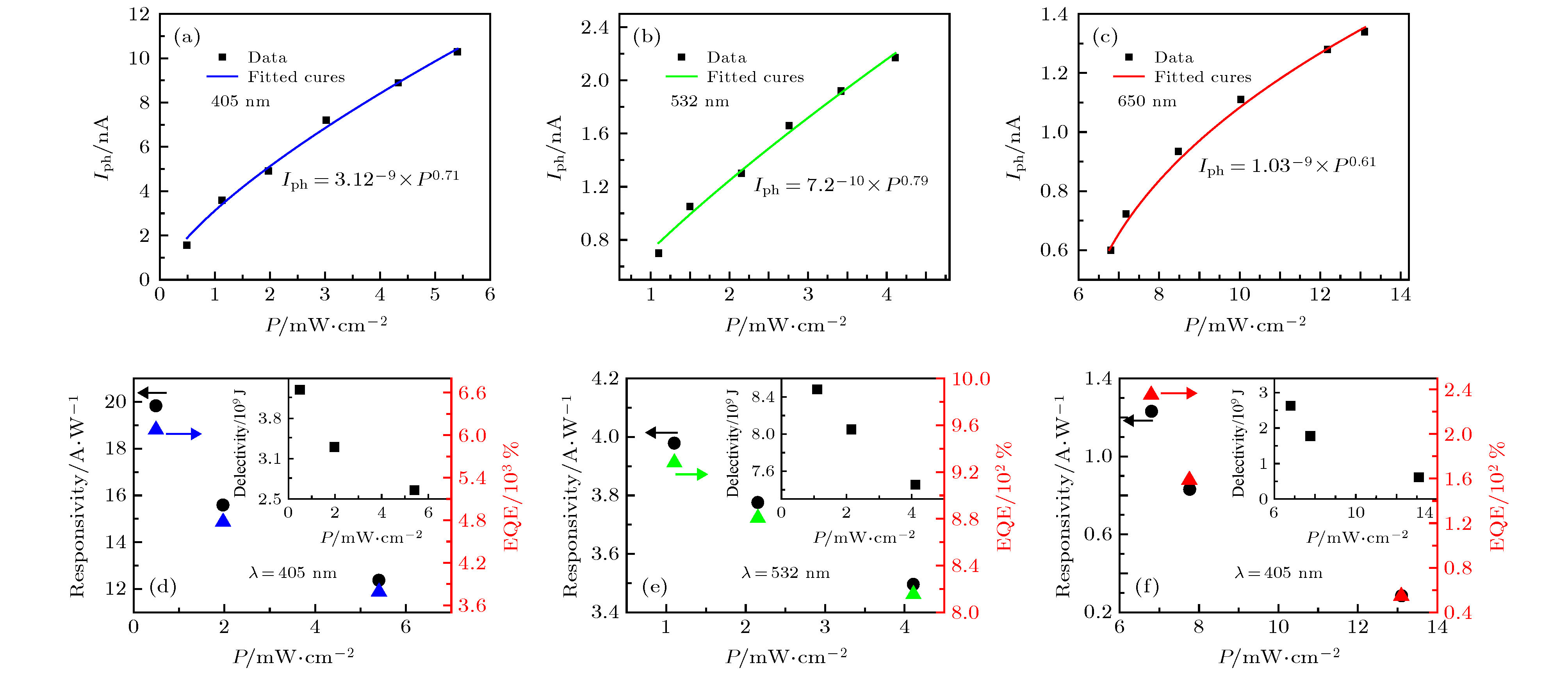
以二硒化锡作为沟道材料, 设计并制备基于二硒化锡场效应晶体管的光电探测器. 以化学气相输运法制备的二硒化锡纯度高且结晶度良好, 对二硒化锡使用机械剥离法制备出层状二硒化锡, 薄膜的横向尺寸最大可达25—35 μm, 最薄厚度仅为1.4 nm, 使用图形转移法制备基于二硒化锡的场效应晶体管, 表面光滑无褶皱, 且表现出良好的电学性质, 呈现出n型半导体的特征, 作为光电探测器对波长分别为405, 532, 650 nm的三基色光表现出明显的光响应. 尤其是对405 nm的蓝紫光响应度最高, 在光强为5.40 mW/cm2时, 响应度达到19.83 AW–1, 外量子效率达到6.07 × 10³ %, 探测率达到4.23 × 10¹⁰ Jones, 并且具有快速的响应速度, 响应反应时间为23.8 ms. 结果表明二硒化锡在可见光光探测器和新一代光电子器件中具有潜在的应用前景.Two dimensional materials have been attracting intensive interest due to their unique physical and optoelectronic properties. As an emerging two dimensional materials, SnSe2 have shown a considerable potential for next-generation electronic and optoelectronic. Herein, SnSe2 bulk crystals have been prepared by a chemical vapour transport method with high purity tin and selenium powder as precursors. Then SnSe2 multilayers has been successfully prepared by a micromechanical exfoliation method from the SnSe2 bulk crystals. The phase structures and elemental composition of the bulk crystal are investigated using an X-Ray diffractometer, an X-ray photoelectrons spectrometer and a Raman spectrometer. And the morphologies are observed using an optical microscope, an atomic force microscope and a transmission electron microscope. The measurement results show that the SnSe2 bulks are single crystals with a high crystallization and purity. The SnSe2 multilayers have a size of 25–35 μm and a thickness of 1.4 nm. To detect the electronic and photoresponse characteristics of the SnSe2 multilayers, a field effect transistor based on such SnSe2 are fabricated via a photolithographic-pattern-transfer method. The transistor has a smooth surface without wrinkles and bubbles, and also has a good contact with Au electrodes. The transistor shows a linear output characteristic and an obvious rectification. The on/off ratio of the device is 47.9 and the electron mobility is 0.25 cm2·V–1·s–1. As a photodetector, the field effect transistor exhibits obvious photoresponse to three visible lights with the wavelengths of 405, 532, and 650 nm. As the lasers are turned on and the device is under illuminations of three visible lights, the current increase rapidly to a saturation state. Then as the lasers are switched off, the current decrease and recover to the original state. The drain-source current can alternate between high and low states rapidly and reversibly, which demonstrates photoresponse characteristics of the devices are stable and sensible. Notably, it shows a strongest response to the 405 nm light at an intensity of 5.4 mW/cm2 with a high responsivity of 19.83 A/W, a good external quantum efficiency of 6.07 × 10³%, a normalized detectivity of 4.23 × 10¹⁰ Jones, and a fast response time of 23.8 ms. The results of this work demonstrate that layered SnSe2 can be a suitable and excellent candidate for visible light photodetector and has a huge potential for high-performance optoelectronic devices.
[1] Novoselov K S, Geim A K, Morozov S V, Jiang D, Zhang Y, Dubonos S V, Grigorieva I V, Firsov A A 2004 Science 306 666
 Google Scholar
[2] Splendiani A, Sun L, Zhang Y B, Li T S, Kim J W, Chim C Y, Galli G L, Wang F 2010 Nano Lett. 10 1271
Google Scholar
[3] Zhou X, Zhang Q, Gan L, Li H Q, Xiong J, Zhai T Y 2016 Adv. Sci. 3 1600177
Google Scholar
[4] Huang Y, Xu K, Shifa A T, Wang Q S, Wang F, Jiang C, He J 2015 Nanoscale 7 17375
Google Scholar
[5] Rai R K, Islam S, Roy A, Agrawal G, Singh A K, Ghosh A, Ravishankar N 2019 Nanoscale 11 870
Google Scholar
[6] Martínez-Escobar D, Ramachandran M, Sánchez-Juárez A, Rios N J S 2013 Thin Solid Films 535 390
Google Scholar
[7] Mukhokosi P E, Krupanidhi S B, Nanda K K 2018 Phys. Status Solidi A 215 1800470
Google Scholar
[8] Moonshik K, Rathi S, Lee I, Li L, Khan M A, Lim D, Lee D, Lee Y, Park J, Pham A T, Duong A T, Cho S, Yun J L, Kim G H 2018 J. Nanosci. Nanotechnol. 18 4243
Google Scholar
[9] Zhou X, Gan L, Tian W M, Zhang Q, Jin S Y, Li H Q, Bando Y, Golberg D, Zhai T Y 2015 Adv. Mater. 27 8035
Google Scholar
[10] Krishna M, Kallatt S 2017 Nanotechnology 29 03250
[11] Wang Q H, Kalantar-Zadeh K, Kis A, Coleman J N, Strano M S 2012 Nat. Nanotechnol. 7 699
Google Scholar
[12] Tian H, Fan C, Liu G Z, Zhang Y H, Wang M J, Li E P 2018 J. Mater. Sci. 54 2059
[13] 郑朝, 孙明轩, 张强, 吴淞要 2018 现代化工 38 122
Zheng Z, Sun M X, Zhang Q, Wu H Y 2018 Mod. Chem. Ind. 38 122
[14] Liu Y, Guo J, Zhu E B, Lee S J, Ding M N, Shakir I, Gambin V, Huang Y, Duan X F 2018 Nature 557 696
Google Scholar
[15] 傅重源, 邢淞, 沈涛, 邰博, 董前民, 舒海波, 梁培 2015 物理学报 64 016102
Google Scholar
Fu Z Y, Xing S, Shen T, Tai B, Dong Q M, Shu H B, Liang P 2015 Acta Phys. Sin. 64 016102
Google Scholar
[16] 孙兰, 张龙, 马飞 2017 中国材料进展 36 40
Sun L, Zhang L, Ma F 2017 Mat-China 36 40
[17] 郑加金, 王雅如, 余柯涵, 徐翔星, 盛雪曦, 胡二涛, 韦玮 2018 物理学报 67 118502
Google Scholar
Zheng J J, Wang Y R, Yu K H, Xv X X, Sheng X X, Hu E T, Wei W 2018 Acta Phys. Sin. 67 118502
Google Scholar
[18] Tan P F, Chen X, Wu L D, Shang Y Y, Liu W W, Pan J, Xiong X 2017 Appl. Catal., B 202 326
Google Scholar
[19] Joensen P, Frindt R F, Morrison S R 1986 Mater. Res. Bull. 21 457
Google Scholar
[20] Feldman Y, Wasserman E, Srolovitz D J, Tenne R 1995 Science 267 222
Google Scholar
[21] Zhou X, Zhang Q, Gan L, Li H Q, Zhai T Y 2016 Adv. Sci. 26 4405
[22] 许宏, 孟蕾, 李杨, 杨天中, 鲍丽宏, 刘国东, 赵林, 刘天生, 邢杰, 高鸿钧, 周兴江, 黄元 2018 物理学报 67 218201
Google Scholar
Xv H, Meng L, Li Y, Yang T Z, Bao L H, Liu G D, Zhao L, Liu T S, Xing J, Gao H J, Zhou X J, Huang Y 2018 Acta Phys. Sin. 67 218201
Google Scholar
-
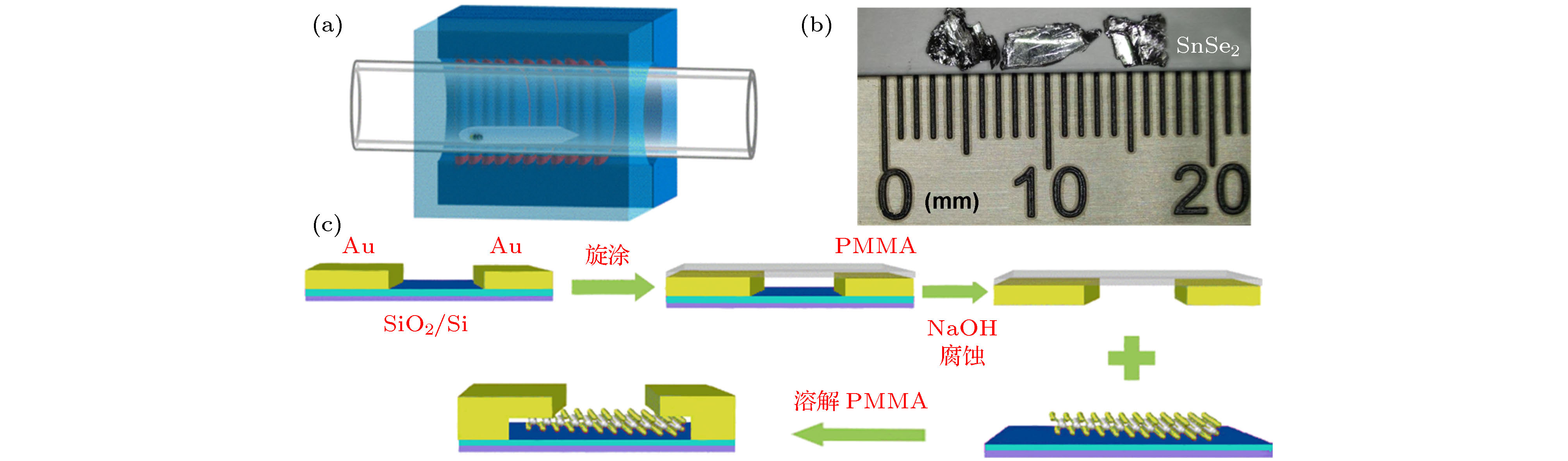
图 1 (a)化学气相输运示意图; (b) SnSe2单晶; (c)图形转移法流程图
Fig. 1. (a) Diagram of CVT; (b) SnSe2 single crystal; (c) Diagram of graph transfer method.

图 4 样品的(a)AFM扫描图象和(b)光学显微图象
Fig. 4. (a) AFM of sample; (b) Optical micro-image of sample.
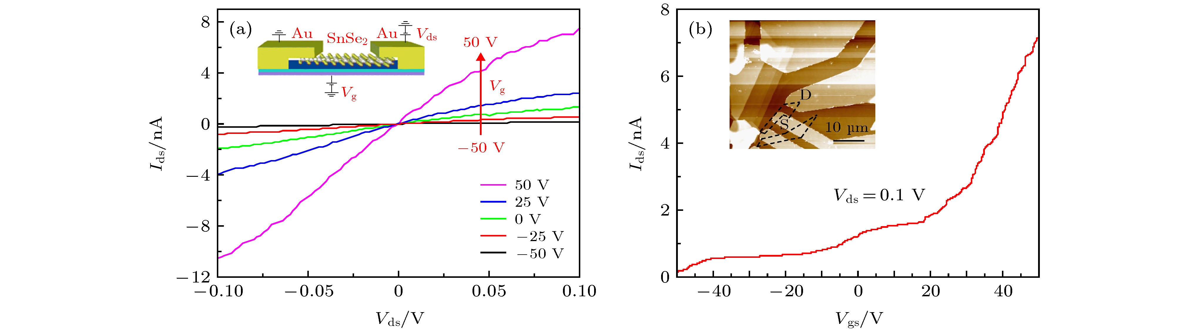
图 6 (a)二维SnSe2场效应晶体管输出特性曲线; (b)器件的转移特性曲线
Fig. 6. (a) Output characteristic of the field effect transistor based on two-dimensional SnSe2; (b) Transfer characteristic of the field effect transistor.

图 7 I-V特性曲线 (a) 405 nm; (b) 532 nm; (c) 650 nm. 光电流曲线 (d) 405 nm; (e) 532 nm; (f) 650 nm. 光响应的上升沿和下降沿 (g) 405 nm; (h) 532 nm; (i) 650 nm
Fig. 7. I-V curve: (a) 405 nm; (b) 532 nm; (c) 650 nm. Photocurrent curve: (d) 405 nm; (e) 532 nm; (f) 650 nm. Rising edge and falling edge: (g) 405 nm; (h) 532 nm; (i) 650 nm.
-
[1] Novoselov K S, Geim A K, Morozov S V, Jiang D, Zhang Y, Dubonos S V, Grigorieva I V, Firsov A A 2004 Science 306 666
Google Scholar
[2] Splendiani A, Sun L, Zhang Y B, Li T S, Kim J W, Chim C Y, Galli G L, Wang F 2010 Nano Lett. 10 1271
Google Scholar
[3] Zhou X, Zhang Q, Gan L, Li H Q, Xiong J, Zhai T Y 2016 Adv. Sci. 3 1600177
Google Scholar
[4] Huang Y, Xu K, Shifa A T, Wang Q S, Wang F, Jiang C, He J 2015 Nanoscale 7 17375
Google Scholar
[5] Rai R K, Islam S, Roy A, Agrawal G, Singh A K, Ghosh A, Ravishankar N 2019 Nanoscale 11 870
Google Scholar
[6] Martínez-Escobar D, Ramachandran M, Sánchez-Juárez A, Rios N J S 2013 Thin Solid Films 535 390
Google Scholar
[7] Mukhokosi P E, Krupanidhi S B, Nanda K K 2018 Phys. Status Solidi A 215 1800470
Google Scholar
[8] Moonshik K, Rathi S, Lee I, Li L, Khan M A, Lim D, Lee D, Lee Y, Park J, Pham A T, Duong A T, Cho S, Yun J L, Kim G H 2018 J. Nanosci. Nanotechnol. 18 4243
Google Scholar
[9] Zhou X, Gan L, Tian W M, Zhang Q, Jin S Y, Li H Q, Bando Y, Golberg D, Zhai T Y 2015 Adv. Mater. 27 8035
Google Scholar
[10] Krishna M, Kallatt S 2017 Nanotechnology 29 03250
[11] Wang Q H, Kalantar-Zadeh K, Kis A, Coleman J N, Strano M S 2012 Nat. Nanotechnol. 7 699
Google Scholar
[12] Tian H, Fan C, Liu G Z, Zhang Y H, Wang M J, Li E P 2018 J. Mater. Sci. 54 2059
[13] 郑朝, 孙明轩, 张强, 吴淞要 2018 现代化工 38 122
Zheng Z, Sun M X, Zhang Q, Wu H Y 2018 Mod. Chem. Ind. 38 122
[14] Liu Y, Guo J, Zhu E B, Lee S J, Ding M N, Shakir I, Gambin V, Huang Y, Duan X F 2018 Nature 557 696
Google Scholar
[15] 傅重源, 邢淞, 沈涛, 邰博, 董前民, 舒海波, 梁培 2015 物理学报 64 016102
Google Scholar
Fu Z Y, Xing S, Shen T, Tai B, Dong Q M, Shu H B, Liang P 2015 Acta Phys. Sin. 64 016102
Google Scholar
[16] 孙兰, 张龙, 马飞 2017 中国材料进展 36 40
Sun L, Zhang L, Ma F 2017 Mat-China 36 40
[17] 郑加金, 王雅如, 余柯涵, 徐翔星, 盛雪曦, 胡二涛, 韦玮 2018 物理学报 67 118502
Google Scholar
Zheng J J, Wang Y R, Yu K H, Xv X X, Sheng X X, Hu E T, Wei W 2018 Acta Phys. Sin. 67 118502
Google Scholar
[18] Tan P F, Chen X, Wu L D, Shang Y Y, Liu W W, Pan J, Xiong X 2017 Appl. Catal., B 202 326
Google Scholar
[19] Joensen P, Frindt R F, Morrison S R 1986 Mater. Res. Bull. 21 457
Google Scholar
[20] Feldman Y, Wasserman E, Srolovitz D J, Tenne R 1995 Science 267 222
Google Scholar
[21] Zhou X, Zhang Q, Gan L, Li H Q, Zhai T Y 2016 Adv. Sci. 26 4405
[22] 许宏, 孟蕾, 李杨, 杨天中, 鲍丽宏, 刘国东, 赵林, 刘天生, 邢杰, 高鸿钧, 周兴江, 黄元 2018 物理学报 67 218201
Google Scholar
Xv H, Meng L, Li Y, Yang T Z, Bao L H, Liu G D, Zhao L, Liu T S, Xing J, Gao H J, Zhou X J, Huang Y 2018 Acta Phys. Sin. 67 218201
Google Scholar

 下载:
下载:

计量
- 文章访问数: 14559
- PDF下载量: 353
- 被引次数: 0
