


-
Due to their superior ability to control light, metasurfaces, ultrathin two-dimensional metamaterials composed of subwavelength nanostructures, have attracted great attention in recent years. Exploring geometric and material freedom in designing elementary nanostructures and their ambient environment of metasurfaces enables versatile optical devices, such as planar metalenses, holographic imaging and thermal radiators. With phase-change materials (PCMs) such as GeSbTe and VO2 integrated into metasurfaces, the optical functionalities of metasurfaces can be flexibly tuned by exploiting the phase transitions of PCMs induced by external stimuli, thereby opening up new directions and perspectives for dynamic tunable metamasurfaces. In this article, we review the recent progress of tunable metasurfaces based on PCMs, analyze their underlying working mechanisms and highlight their important applications. We conclude this review by bringing our perspectives on challenges and future directions in this field.
-
Keywords:
- metasurfaces /
- phase-change materials /
- nanophotonics /
- active modulation
[1] Chen H T, Taylor A J, Yu N 2016 Rep. Prog. Phys. 79 076401
 Google Scholar
[2] Kadic M, Milton G W, van Hecke M, Wegener M 2019 Nat. Rev. Phys. 1 198
Google Scholar
[3] Shalaev V M 2007 Nat. Photonics 1 41
Google Scholar
[4] Alam M Z, Schulz S A, Upham J, De Leon Robert I, Boyd R W 2018 Nat. Photonics 12 79
Google Scholar
[5] Ma Q, Hu H, Huang E, Liu Z 2017 Nanoscale 9 18268
Google Scholar
[6] Schurig D, Mock J J, Justice B J, Cummer S A, Pendry J B, Starr A F, Smith D R 2006 Science 314 977
Google Scholar
[7] Ma Q, Cui T J 2020 PhotoniX 1 1
Google Scholar
[8] Meinzer N, Barnes W L, Hooper I R 2014 Nat. Photonics 8 889
Google Scholar
[9] Arbabi A, Arbabi E, Horie Y, Kamali S M, Faraon A 2017 Nat. Photonics 11 415
Google Scholar
[10] Monticone F, Estakhri N M, Alù A 2013 Phys. Rev. Lett. 110 203903
Google Scholar
[11] Novotny L, van Hulst N 2011 Nat. Photonics 5 83
Google Scholar
[12] Bharadwaj P, Deutsch B, Novotny L 2009 Adv. Opt. Photonics 1 438
Google Scholar
[13] Maier S A 2007 Plasmonics: Fundamentals and Applications (New York: Springer Science + Business Media LLC) pp65–88
[14] Yu N, Genevet P, Kats M A, Aieta F, Tetienne J P, Capasso F, Gaburro Z 2011 Science 334 333
Google Scholar
[15] Sun S, He Q, Xiao S, Xu Q, Li X, Zhou L 2012 Nat. Mater. 11 426
Google Scholar
[16] Ee H S, Agarwal R 2016 Nano Lett. 16 2818
Google Scholar
[17] Sautter J, Staude I, Decker M, Rusak E, Neshev D N, Brener I, Kivshar Y S 2015 ACS Nano 9 4308
Google Scholar
[18] Yao Y, Shankar R, Kats M A, Song Y, Kong J, Loncar M, Capasso F 2014 Nano Lett. 14 6526
Google Scholar
[19] Wang Q, Rogers E T F, Gholipour B, Wang C M, Yuan G, Teng J, Zheludev N I 2016 Nat. Photonics 10 60
Google Scholar
[20] Wuttig M, Bhaskaran H, Taubner T 2017 Nat. Photonics 11 465
Google Scholar
[21] Salinga M, Kersting B, Ronneberger I, Jonnalagadda V P, Vu X T, Le Gallo M, Giannopoulos I, Cojocaru Mirédin O, Mazzarello R, Sebastian A 2018 Nat. Mater. 17 681
Google Scholar
[22] Hosseini P, Wright C D, Bhaskaran H 2014 Nature 511 206
Google Scholar
[23] Du K K, Li Q, Lyu Y B, Ding J C, Lu Y, Cheng Z Y, Qiu M 2017 Light Sci. Appl. 6 e16194
Google Scholar
[24] Ríos C, Stegmaier M, Hosseini P, Wang D, Scherer T, Wright C D, Bhaskaran H, Pernice W H P 2015 Nat. Photonics 9 725
Google Scholar
[25] Feldmann J, Stegmaier M, Gruhler N, Ríos C, Bhaskaran H, Wright C D, Pernice W H P 2017 Nat. Commun. 8 1256
Google Scholar
[26] Qu Y R, Li Q, Du K K, Cai L, Lu J, Qiu M 2017 Laser Photonics Rev. 11 1700091
Google Scholar
[27] Tittl A, Michel A K U, Schäferling M, Yin X, Gholipour B, Cui L, Wuttig M, Taubner T, Neubrech F, Giessen H 2015 Adv. Mater. 27 4597
Google Scholar
[28] Tian J Y, Luo H, Yang Y Q, Ding F, Qu Y R, Zhao D, Qiu M, Bozhevonyi S I 2019 Nat. Commun. 10 396
Google Scholar
[29] Chen Y G, Kao T S, Ng B, Li X, Luo X G, Luk’yanchuk B, Maier A, Hong M H 2013 Opt. Express 21 13691
Google Scholar
[30] Yin X, Schäferling M, Michel A K U, Tittl A, Wuttig M, Taubner T, Giessen H 2015 Nano Lett. 15 4255
Google Scholar
[31] Michel A K U, Zalden P, Chigrin D N, Wuttig M, Lindenberg A M, Taubner T 2014 ACS Photonics 1 833
Google Scholar
[32] Michel A K U, Chigrin D N, Maß T W W, Schönauer K, Salinga M, Wuttig M, Taubner T 2013 Nano Lett. 13 3470
Google Scholar
[33] Gholipour B, Zhang J, Macdonald K F, Hewak D W, Zheludev N I 2013 Adv. Mater. 25 3050
Google Scholar
[34] Yin X, Steinle T, HuangL, Taubner T, Wuttig M, Zentgraf T, Giessen H 2017 Light Sci. Appl. 6 e17016
Google Scholar
[35] De Galarreta C R, Alexeev A M, Au Y Y, Lopez Garcia M, Klemm M, Cryan M, Bertolotti J, Wright C D 2018 Adv. Funct. Mater. 28 1704993
Google Scholar
[36] Chaudhary K, Tamagnone M, Yin X, Spägele C M, Oscurato S L, Li J, Persch C, Li R, Rubin N A, Jauregui L A, Watanabe K, Taniguchi T, Kim P, Wuttig M, Edgar J H, Ambrosio A, Capasso F 2019 Nat. Commun. 10 4487
Google Scholar
[37] Bai W, Yang P, Wang S, Huang J, Chen D, Zhang Z, Yang J, Xu B 2019 Nanomaterials 9 993
Google Scholar
[38] Ding F, Pors A, Bozhevolnyi S I 2018 Rep. Prog. Phys. 81 026401
Google Scholar
[39] de Abajo F J G 2007 Rev. Mod. Phys. 79 1267
Google Scholar
[40] Zhang J, ElKabbash M, Wei R, Singh S C, Lam B, Guo C 2019 Light Sci. Appl. 8 53
Google Scholar
[41] Wang J, Butet J, Bernasconi G D, Baudrion A L, Lévêque G, Horrer A, Horneber A, Martin O J F, Meixner A J, Fleischer M, Adam P M, Zhang D 2019 Nanoscale 11 23475
Google Scholar
[42] Wang J, Butet J, Baudrion A L, Horrer A, Lévêque G, Martin O J F, Meixner A J, Fleischer M, Adam P M, Horneber A, Zhang D 2016 J. Phys. Chem. C 120 17699
Google Scholar
[43] Wang J, Gürdal E, Horneber A, Dickreuter S, Kostcheev S, Meixner A J, Fleischer M, Adam P M, Zhang D 2018 Nanoscale 10 8240
Google Scholar
[44] Palomba S, Novotny L 2008 Phys. Rev. Lett. 101 056802
Google Scholar
[45] Lalanne P, Astilean S, Chavel P, Cambril E, Launois H 1999 J. Opt. Soc. Am. A 16 1143
Google Scholar
[46] Khorasaninejad M, Chen W T, Devlin R C, Oh J, Zhu A Y, Capasso F 2016 Science 352 1190
Google Scholar
[47] Atwater H A, Polman A 2010 Nat. Mater. 9 205
Google Scholar
[48] Hao J, Yuan Y, Ran L, Jiang T, Kong J A, Chan C T, Zhou L 2007 Phys. Rev. Lett. 99 063908
Google Scholar
[49] Hao J, Ren Q, An Z, Huang X, Chen Z, Qiu M, Zhou L 2009 Phys. Rev. A 80 023807
Google Scholar
[50] Liu W, Chen S, Li Z, Cheng H, Yu P, Li J, Tian J 2015 Opt. Lett. 40 3185
Google Scholar
[51] Liu B, Chen S, Zhang J, Yao X, Zhong J, Lin H, Huang T, Yang Z, Zhu J, Liu S, Lienau C, Wang L, Ren B 2018 Adv. Mater. 30 1706031
Google Scholar
[52] Luo H, Li Q, Du K, Xu Z, Zhu H, Liu D, Cai L, Ghosh P, Qiu M 2019 Nano Energy 65 103998
Google Scholar
[53] Wang J, Coillet A, Demichel O, Wang Z, Rego D, Bouhelier A, Grelu P, Cluzel B 2020 Light Sci. Appl. 9 50
Google Scholar
[54] Wang S, Wu P C, Su V C, Lai Y C, Chu C H, Chen J W, Lu S H, Chen J, Xu B, Kuan C H, Li T, Zhu S, Tsai D P 2017 Nat. Commun. 8 187
Google Scholar
[55] Wang S, Wu P C, Su V C, Lai Y C, Chen M K, Kuo H Y, Chen B H, Chen Y H, Huang T T, Wang J H, Lin R M, Kuan C H, Li T, Wang Z, Zhu S, Tsai D P 2018 Nat. Nanotechnol. 13 227
Google Scholar
[56] Arbabi E, Arbabi A, Kamali S M, Horie Y, Faraji Dana M, Faraon A 2018 Nat. Commun. 9 812
Google Scholar
[57] Zhao Y, Alù A 2013 Nano Lett. 13 1086
Google Scholar
[58] Arbabi A, Horie Y, Bagheri M, Faraon A 2015 Nat. Nanotechnol. 10 937
Google Scholar
[59] Liu W, Li Z, Li Z, Cheng H, Tang C, Li J, Chen S, Tian J 2019 Adv. Mater. 31 1901729
Google Scholar
[60] Shalaev M I, Sun J, Tsukernik A, Pandey A, Nikolskiy K, Litchinitser N M 2015 Nano Lett. 15 6261
Google Scholar
[61] Kang L, Jekins R P, Werner D H 2019 Adv. Opt. Mater. 7 1801813
Google Scholar
[62] Hail C U, Michel A K U, Poulikakos D, Eghlidi H 2019 Adv. Opt. Mater. 7 1801786
Google Scholar
[63] Cui T, Bai B, Sun H B 2019 Adv. Funct. Mater. 29 1806692
Google Scholar
[64] Goi E, Zhang Q, Chen X, Luan H, Gu M 2020 Photoni X 1 3
Google Scholar
[65] Shportko K, Kremers S, Woda M, Lencer D, Robertson J, Wuttig M 2008 Nat. Mater. 7 653
Google Scholar
[66] Park J W, Eom S H, Lee H, Da Silva J L, Kang Y S, Lee T Y, Khang Y H 2009 Phys. Rev. B 80 115209
Google Scholar
[67] Pan M Y, Huang Y, Li Q, Luo H, Zhu H Z, Kaur S, Qiu M 2020 Nano Energy 69 104449
Google Scholar
[68] Gholipour B, Karvounis A, Yin J, Soci C, Macdonald K F, Zheludev N I 2018 NPG Asia Mater. 10 533
Google Scholar
[69] Li P, Yang X, Maß T W W, Hanss J, Lewin M, Michel A K U, Wuttig M, Taubner T 2016 Nat. Mater. 15 870
Google Scholar
[70] Eyert V 2002 Ann. Phys. 11 650
Google Scholar
[71] Dicken M J, Aydin K, Pryce I M, Swetlock L A, Boyd E M, Walavalker S, Ma J, Atwater H A 2009 Opt. Express 17 18330
Google Scholar
[72] Xu Z, Li Q, Du K, Long S, Yang Y, Cao X, Luo H, Zhu H, Ghosh P, Shen W, Qiu M 2020 Laser Photonics Rev. 14 1900162
Google Scholar
[73] Lalanne P, Yan W, Kevin V, Sauvan C, Hugonin J P 2018 Laser Photonics Rev. 12 1700113
Google Scholar
[74] Weiss T, Mesch M, Schäferling M, Giessen H, Langbein W, Mulfarov E A 2016 Phys. Rev. Lett. 116 237401
Google Scholar
[75] Kats M A, Blanchard R, Genevet P, Yang Z, Qazilbash M M, Basov D N, Ramanathan S, Capasso F 2013 Opt. Lett. 38 368
Google Scholar
[76] Shu F, Yu F, Peng R, Zhu Y, Xiong B, Fan R, Wang Z, Liu Y, Wang M 2018 Adv. Opt. Mater. 6 1700939
Google Scholar
[77] Song S, Ma X, Pu M, Li X, Guo Y, Gao P, Luo X 2018 Photonics Res. 6 492
Google Scholar
[78] Jia Z, Shu F, Gao Y, Cheng F, Peng R, Fan R, Liu Y, Wang M 2018 Phys. Rev. Appl. 9 034009
Google Scholar
[79] Liu L, Kang L, Mayer T S, Werner D H 2016 Nat. Commun. 7 13236
Google Scholar
[80] Lei D, Appavoo K, Ligmajer F, Sonnefraud Y, Haglund R F, Maier S A 2015 ACS Photonics 2 1306
Google Scholar
[81] Tian J Y, Li Q, Lu J, Qiu M 2018 Opt. Express 26 23918
Google Scholar
[82] Qu Y R, Li Q, Cai L, Pan M Y, Ghosh P, Du K K, Qiu M 2018 Light Sci. Appl. 7 26
Google Scholar
[83] Cavalleri A, Tóth C, Siders C W, Squier J A, Ráksi F, Forget P, Kieffer J C 2001 Phys. Rev. Lett. 87 237401
Google Scholar
[84] Jager M F, Ott C, Kraus P M, Kaplan C J, Pouse W, Marvel R E, Haglund R F, Neumark D M, Leone S R 2017 Proc. Natl. Acad. Sci. U.S.A. 114 9558
Google Scholar
-
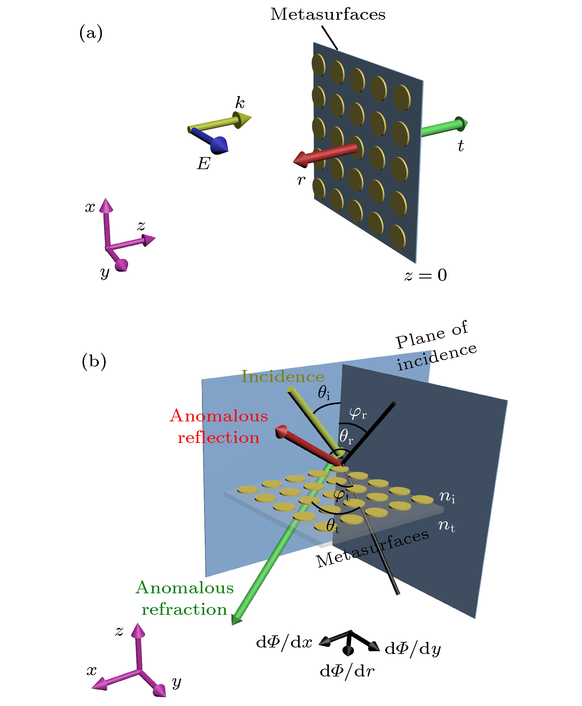
图 1 超表面光调控的原理 (a)光通过超表面后透射(t, 绿色箭头)和反射系数(r, 红色箭头)的计算模型; (b)广义的折射和反射公式; 其中棕色、红色和绿色箭头分别表示入射、反射和折射波矢方向, 黑线表示波矢在与入射平面相垂直的平面的投影
Fig. 1. Principle of light modulation with metasurfaces: (a) Light transmission (green arrow) and reflection (red arrow) through a metasurface; (b) the generalized Snell’s law of reflection and refraction. Brown, red and green arrows represent the propagation directions of incident, reflected and refracted light, respectively. Black lines represent the projections of wavevectors of reflected and refracted light onto the surface perpendicular to the plane of incidence.
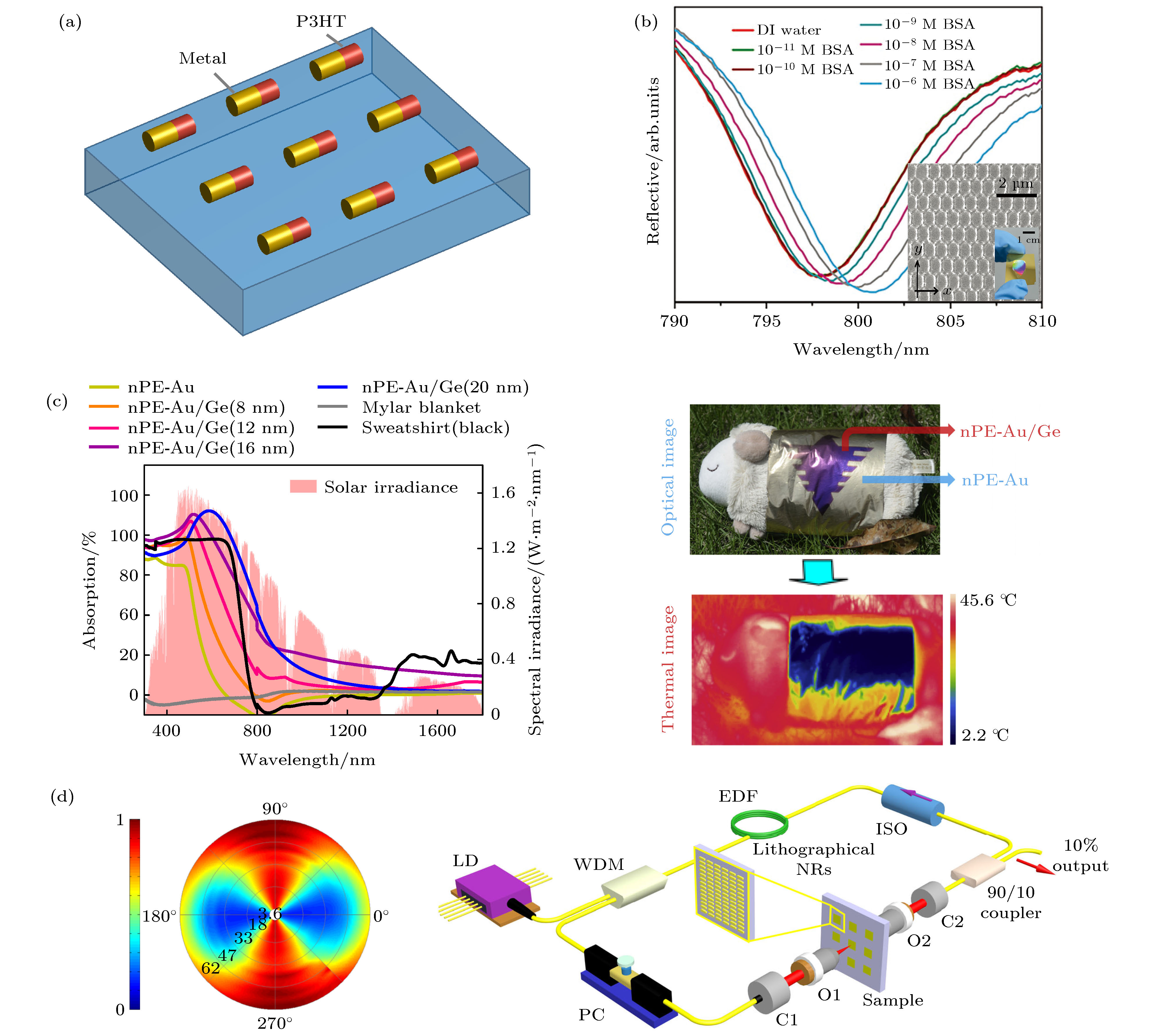
图 2 超表面在调控光波振幅上的前沿应用 (a)等离激元超表面增强的有机太阳能电池[47]; (b)基于等离激元超表面的液体浓度传感器, 右下角是正六边形金超表面的扫描电子显微镜图片和实物图(1 M = 1 mol/L)[51]; (c)超表面多层带孔薄膜保暖织物[52]; 左侧: 不同镀膜厚度nPE-Au/Ge超表面的吸收光谱, 右侧: 带有nPE-Au/Ge超表面的一实物在可见(上)和红外(下)波段的成像; (d)基于等离激元超表面的孤子锁模激光器[53]; 左侧: 金纳米棒超表面在1550 nm激发光下的光学透过率随激发光功率和偏振变化的实验数据伪彩图, 径向表示激光功率, 方位角表示偏振方向, 颜色表示光透过率; 右侧: 电子束刻蚀的纳米金棒超表面用作可饱和吸收体集成于超短脉冲光纤激光器谐振腔中; LD, 激光二极管; WDM, 波分复用器; EDF, 掺铒光纤; ISO, 光频隔离器; PC, 偏振控制器; C1, C2, 准直器; O1, O2, 物镜
Fig. 2. Applications of metasurfaces based on modulation of light in amplitude. (a) Efficiency improvement of organic solar cell by exploiting plasmonic metasurfaces[47]. (b) Liquid concentration sensor based on plasmonic metasurfaces[51]. Inset: scanning electron microscope (SEM) and optical images of a gold hexagonal-lattice metasurface. (c) Ultra-thin colored textile with simultaneous solar and passive heating abilities[52]. Left: measured absorptivity of different textiles from visible to near infrared wavelength; Right: optical and thermal images of a toy sheep partly wearing a colored textile. (d) Ultrafast pulsed fiber laser using lithographically-defined plasmonic metasurfaces as saturable absorbers[53]. Left: experimental excitation power and polarization dependent nonlinear transmittance of a gold nanorod metasurface; Right: sketch of the home-built ultrafast fiber laser integrating lithographical plasmonic metasurfaces as saturable absorbers; laser diode (LD), wavelength-division multiplexing (WDM), erbium-doped fiber (EDF), optical isolator (ISO), polarization controller (PC), collimators (C1, C2) and objectives (O1, O2).
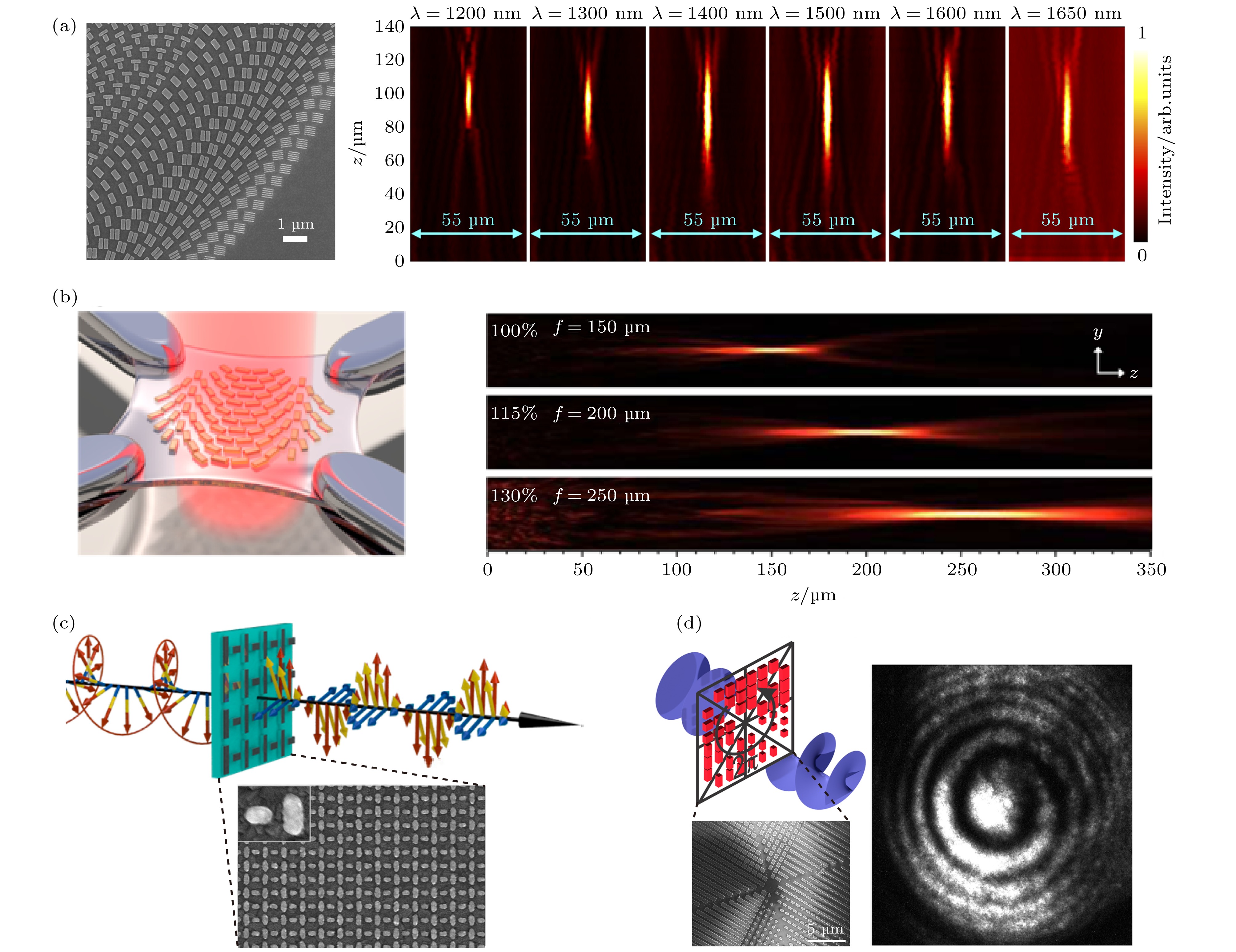
图 3 超表面在调控光波相位上的前沿应用 (a)具有色散校正功能的平面透镜[54]; 左侧: 扫描电子显微镜镜图像(比例尺是1 μm); 右侧: 平面透镜在不同波长下的聚焦光斑; (b)柔性超表面透镜[16]; 左侧: 微机械拉伸柔性衬底上的平面透镜以实现变焦; 右侧: 拉伸量在100%, 115%和130%时平面透镜的焦距分别为150, 200和250 μm; (c)超表面将圆偏振光转变为线偏振[57]; (d)超表面把线偏振光转变成螺旋光[60]
Fig. 3. Applications of metasurfaces based on modulation of light in phase. (a) Broadband achromatic metalens[54]. Left: SEM image of the metalens (scale bar, 1 μm); Right: measured light intensity profiles for the achromatic metalens at various incident wavelengths. (b) Zoom metalens on a stretchable substrate[16]. Left: sketch of a metasurface on a stretched PDMS membrane; Right: measured longitudinal beam profiles generated on the transmission side of the zoom metalens with stretch factor s = 100% (top), 115% (middle), and 130% (bottom). (c) Ultrathin quarter-wave meta-plate for circular-linear polarization conversion[57]. (d) Dielectric-metasurface enabled optical vortex beam converter[60].

图 4 (a)晶态与非晶态GST-225的相变过程; 当温度超过结晶温度160 ℃, 非晶态GST (a-GST)相变为晶态GST (c-GST); 当温度升至熔点640 ℃, c-GST液化, 后经快速冷却可形成a-GST; (b)晶态与非晶态GST-225的介电常数[65,66]
Fig. 4. (a) Sketch of phase transitions between crystalline and amorphous phases of GST-225; (b) dielectric permittivity of crystalline and amorphous GST-255[65,66].
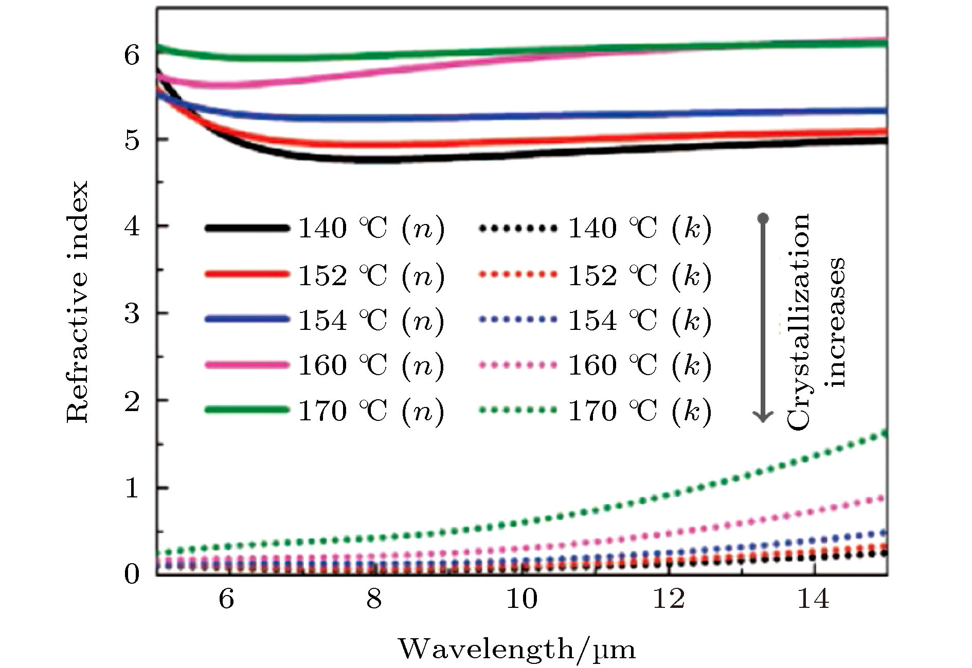
图 5 GST-225薄膜在不同加热温度下的折射率[23]; GST-225薄膜的厚度为450 nm当温度从140 ℃逐渐增至170 ℃时, 晶态GST的比例不断增加, 材料的射率实部n (实线)与虚部k (虚线)逐渐变大趋近晶态GST的折射率
Fig. 5. Measured refractive index of a 450-nm thick GST-225 film at different temperatures[23]. As the heating temperature increases from 140 ℃ to 170 ℃, the degree of GST-225 crystallinity increases, and, accordingly, both the real (solid line) and imaginary parts (dashed lines) of the refractive index increase and approach the values of crystalline GST-225.
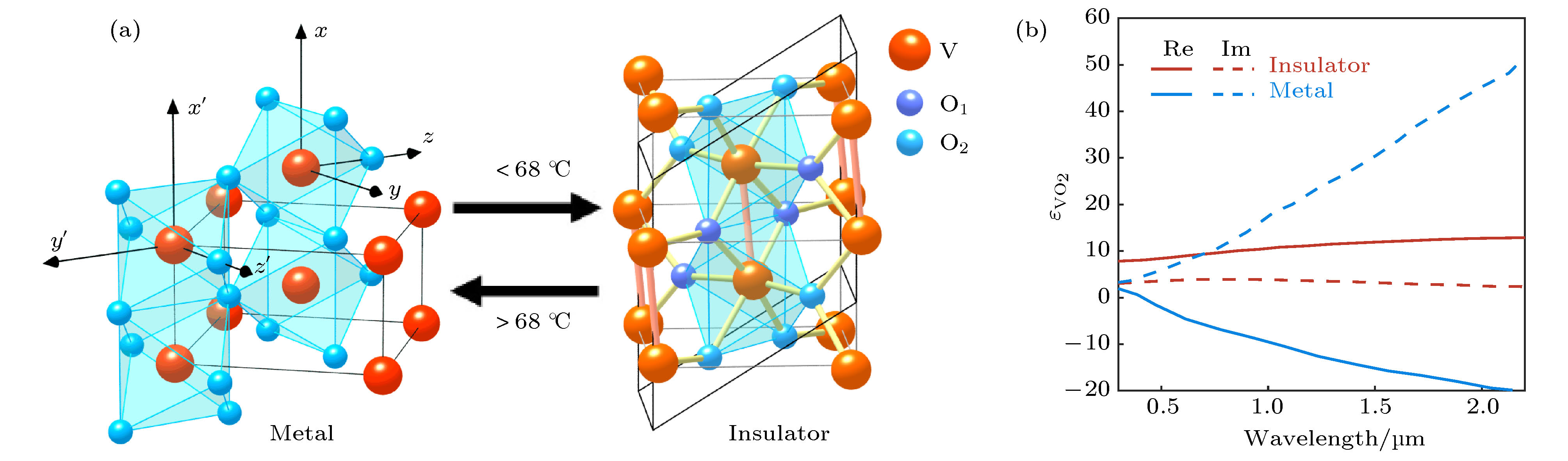

图 7 GST-225圆柱体微纳结构在两种晶态下的光学响应 (a)非晶态(蓝色区域)和晶态GST-225 (红色区域)圆柱体微纳结构的消光截面光谱, 圆柱体半径为1 μm, 高度为500 nm; (b) GST-225圆柱体微纳结构谐振模式的复频率,
$ \tilde {\omega }\equiv \varOmega -\mathrm{i}\varGamma /2 $ ; 蓝色标记对应非晶态, 红色标记对应晶态; (c)非晶态GST-225圆柱体微纳结构的Ez模场分布, 其中z是圆柱体的轴向(高度)方向Fig. 7. Optical responses of a GST-225 nanorod in the amorphous and crystalline phases. The rod has a radius of 1 μm and a height of 500 nm. (a) Extinction-cross-section spectra of the amorphous (blue area) and crystalline (red area) GST-225 rod illuminated by a plane wave. (b) Eigenfrequencies,
$ \tilde {\omega }\equiv \varOmega -\mathrm{i}\varGamma /2 $ , of three dominant resonance modes. Blue and red markers correspond to the GST-225 rod in the amorphous and crystalline phases, respectively. (c) Real part of Ez (z component of electric field) distributions of three modes of the amorphous GST-225 rod.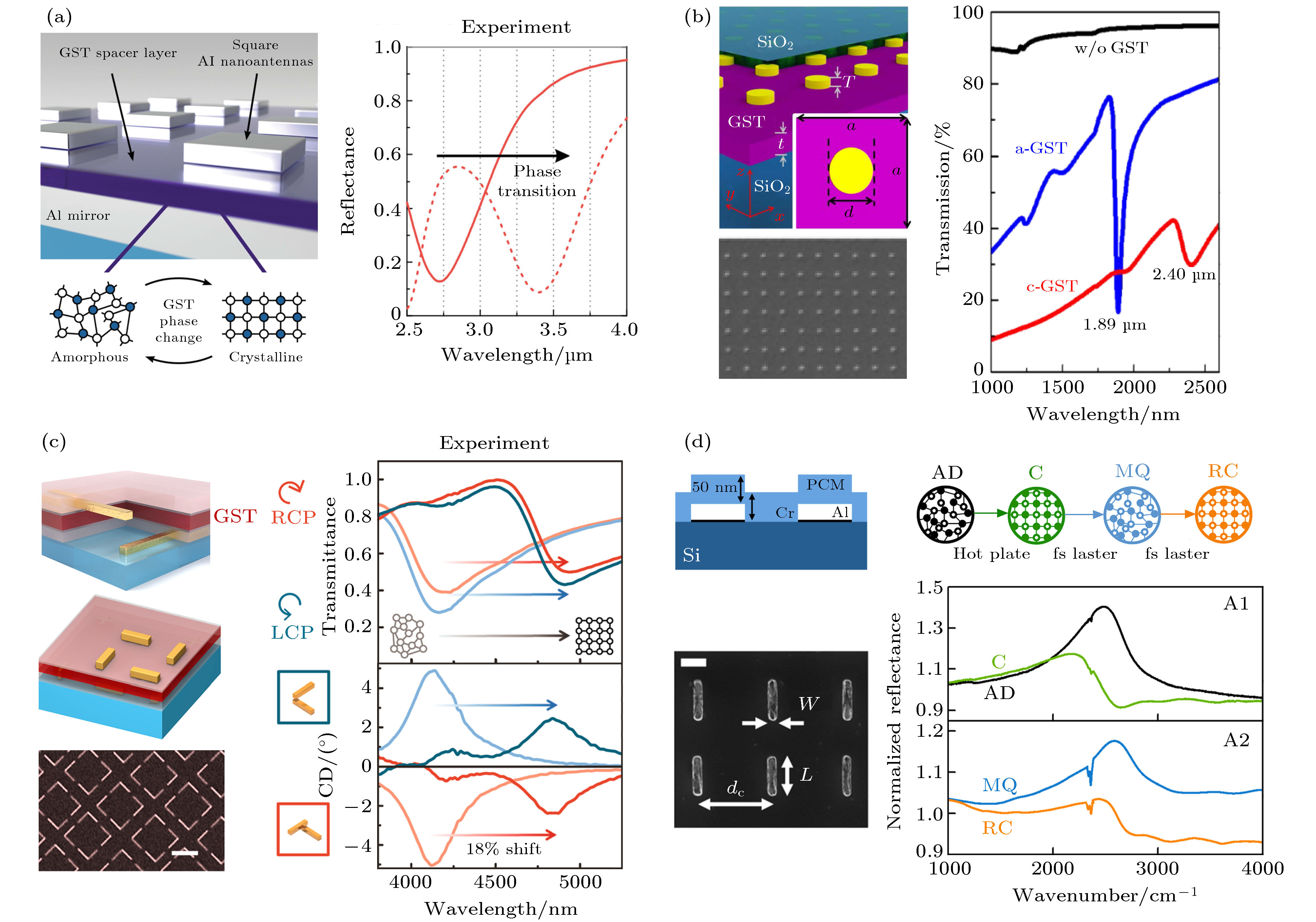
图 8 结合GST和表面等离激元超表面的振幅调控 (a)基于表面等离激元超表面的可调完美吸收器[27]; 左侧: 超表面结构示意图; 右侧: GST-326不同相态下的反射光谱, 谱谷对应最大吸收率; (b)表面等离激元超表面透射光谱的动态调控[29]; 左侧: 超表面结构示意图和扫描电子显微镜图片; 右侧: GST-225不同相态下的反射光谱; (c)结合GST和表面等离激元的可调手性超表面[30]; 左侧: 超表面结构示意图和扫描电子显微镜图片; 右侧: GST-326在不同相态和不同圆偏振态下的透射光谱以及圆二色光谱; (d)基于激光脉冲对超表面反射光谱的动态调控[31]; 左侧: 超表面结构示意图和扫描电子显微镜图片; 右侧: GST-326不同相态下的反射光谱; “AD”表示初始非晶态GST-326; “C”表示经加热后的晶态GST-326; “MQ”表示强功率单激光脉冲照射下由晶态GST-326转化的非晶态GST-326; “RC”表示经弱功率多脉冲激光照射下由非晶态GST-326转化的晶态GST-326
Fig. 8. Active modulation of light in amplitude by integrating phase-change material GST into plasmonic metasurfaces. (a) Tunable perfect absorber[27]. Left: sketch of the device; Right: measured reflectance spectra of the metasurface for the GST-326 layer in the amorphous (solid line) and crystalline (dashed line) phases. (b) Plasmonic metasurface with tunable transmittance[29]. Left: sketch of the device; Right: calculated transmittance spectra of the metasurface for the GST-225 layer in the amorphous (blue line) and crystalline (red line) phases. (c) Tunable chiral metasurfaces[30]. Left: sketch and SEM image of the device; Right: measured transmittance and CD spectra of the metasurface for the GST-326 layer in the amorphous (lighter curves) and crystalline (darker curves) phases. (d) Optical switching of reflectance spectra using femtosecond laser pulses[31]. Left: sketch and SEM image of the metasurface; Right: measured reflectance spectra of the metasurface for the GST-326 layer in different phases—as-deposited amorphous phase (AD), thermally crystallized (C) phase, optically reamorphized (MQ) phase, and optically recrystallized (RC) phase
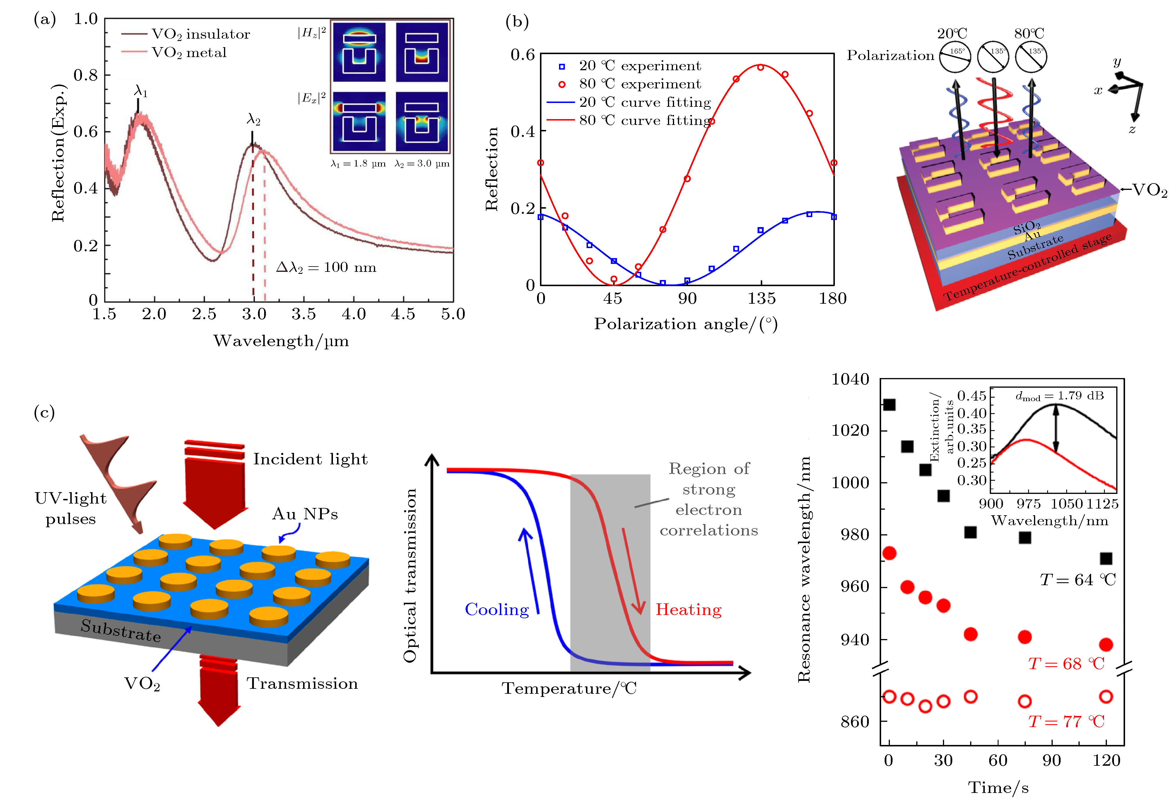
图 9 结合VO2和表面等离激元超表面的振幅调控 (a)表面等离激元超表面反射光谱的动态调控[71]; 插图:
$ {\left|{H}_{z}\right|}^{2} $ 与$ {\left|{E}_{x}\right|}^{2} $ 在谐振波长处的空间分布图(VO2处于绝缘态); (b)基于表面等离激元超表面的动态可调偏振片[78]; 左侧: 反射系数随(放置于超表面结构前)偏振片角度变化的曲线; 右侧: 器件的原理图; (c)紫外激光脉冲照射VO2实现对超表面的动态调控[80]; 左侧: 器件的原理图; 中间: 超表面透射率与VO2温度的关系示意图; 右侧: 表面等离谐振波长随紫外激光脉冲照射时间的变化关系Fig. 9. Active modulation of light in amplitude by integrating phase-change material VO2 into plasmonic metasurfaces. (a) Plasmonic metasurface with tunable relfectance[71]. Inset:
$ {\left|{H}_{z}\right|}^{2} $ and$ {\left|{E}_{x}\right|}^{2} $ distributions at the resonant wavlengthwith VO2 in the insulator phase. (b) Tunnable plasmonic-metasurface polarizer[78]. Left: reflectance of the sample as a function of the polarizer angle (put in front of the metasurface) at 3 μm wavelength for VO2 at 20 ℃ and 80 ℃; Right: sketch of the device. (c) Optical switching of transmittance spectra with UV laser pulses[80]. Left: sketch of the device; Middle: hysteretic response in the transmttiance during the heating cycle of the phase transition of VO2; Right: plasmon resonance wavelength of the Au nanodisks of 175-nm diameter on the VO2 film as a function of the total UV illumination time, while the whole sample was thermally latched at two different temperatures within the phase transition region, 64 ℃ (blacksquares) and 68 ℃ (red circles), and also above (77 ℃, red empty circles).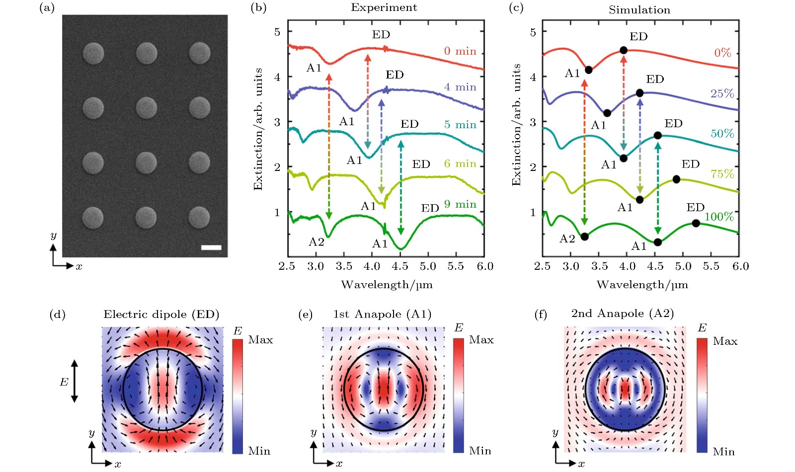
图 10 基于米氏谐振的GST超表面[28] (a) GST-225盘状微结构的扫描电子显微镜图像, 图中比例尺代表2 μm; (b), (c)不同晶化比例下GST盘状结构的实验(b)和理论(c)消光光谱, 其中A1和A2代表一阶和二阶环形电磁场态, ED代表电偶极子; (d)−(f) 非晶态GST-255在ED, A1, A2模式的电场强度分布(颜色代表电场强度, 箭头代表电场方向)
Fig. 10. Tunable metasurface composed of GST nanodisk arrays[28]. (a) SEM image of GST disks. The scale bar represents 2 μm. (b) Experimental and (c) simulated extinction spectra of disk arrays with a radius of 1 μm and a height of H = 220 nm. A1 and A2 denotes the 1st- and 2nd-order anapole states, respectively. (d)−(f) Simulated near-field distributions of the ED (electric dipole resonance), and A1 and A2 states.
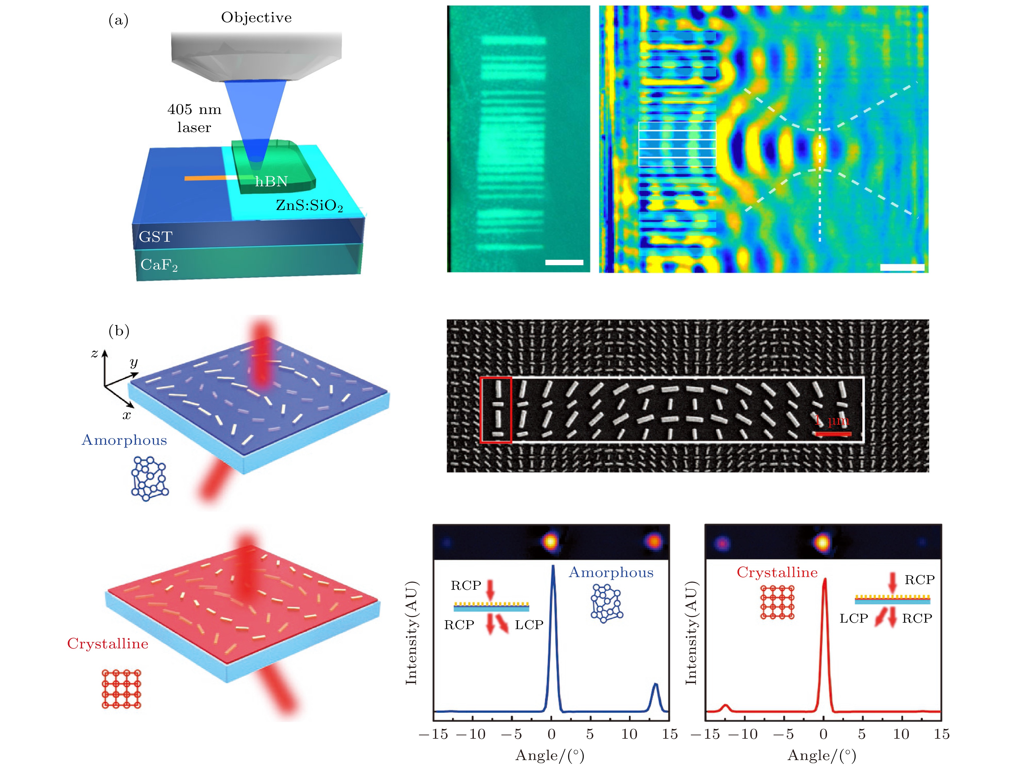
图 11 基于相变材料和表面等离激元超表面的平面透镜和光束偏转器 (a)激光直写GST-326声子极化激元超表面透镜[36]; 左侧: 激光直写示意图; 右侧: 超表面透镜的光学图像(明暗区域分别对应晶态与非晶态GST), 以及其对hBN支持的声子极化激元的聚焦光场分布; (b)基于GST-326超表面可调光束偏转器[34]; 左侧: 器件功能示意图; 右上: 器件的扫描电子显微镜图片; 右下: GST-326两种相态下的透射光强的角度分布
Fig. 11. Tunable metalens and beam switcher based on phase-change materials. (a) Flat polaritonic lenses optically written in a GST-326 film below a hBN film[36]. Left: optical images of the laser-written metalens; Right: s-SNOM image of the metalens showing focusing of polaritons at 1445 cm–1. (b) Beam switcher composed of a plasmonic metasurface above a GST-226 layer[34]. Left: sketch of the device; Top right: SEM image of the device; Bottom right: infrared camera images and intensity plots of the beam transmitted through the device for the GST-226 layer in the amorphous (left) and crystalline (right) phases.
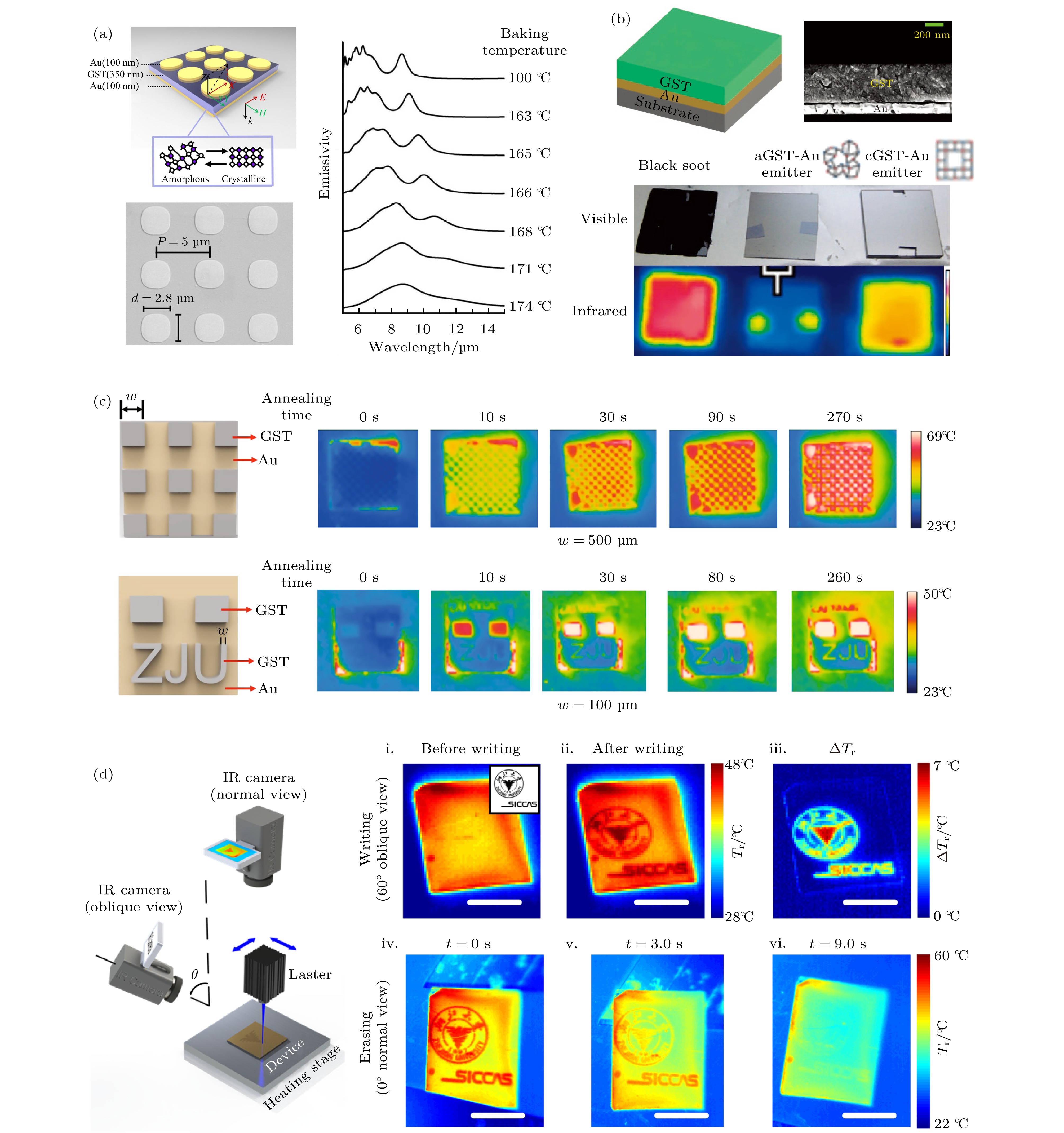
图 12 基于相变材料的可调热辐射器 (a)基于GST-225和表面等离激元超表面可调热辐射器[26]; 左侧: 超表面结构示意图与扫描电子显微镜图片; 右侧: 在不同温度下器件的热辐射光谱; (b)基于GST-225薄膜结构的可调热辐射器[23]; 上方: 薄膜结构示意图和扫描电子显微镜图片; 下方: 晶态GST薄膜、非晶态GST薄膜和熏黑的不锈钢切片的可见光(上排)与红外(下排)照片; (c) GST-225薄膜热辐射器用于红外“隐身”和图像增强[82]; 左侧: GST-225薄膜构成的棋盘图案和“ZJU”图案示意图; 右侧: 通过加热控制VO2导体态比例得到不同的红外热图像; (d)激光直写VO2重构热图像[72]; 左侧: 实验装置示意图; 右上侧: 激光直写浙江大学徽标的热图像; 右下侧: 降低VO2温度, 热图像消失
Fig. 12. Tunable thermal emitters based on phase-change materials. (a) An ultrathin meta-insulator-metal plasmonic thermal emitter incorporating GST-225[26]. Left: sketch and SEM image of the device; Right: experimental results of continuously tuning emissivities of the thermal emitter at different baking temperatures. (b) Tunable thermal emitter composed of a GST-225 film on top of a gold film[23]. Top: sketch and SEM image of the thermal emitter; Bottom: visible and infrared photographs of the black soot (left), the amorphous-GST-Au emitter (middle) and the crystalline-GST-Au emitter (right) at 100 ℃. (c) Thermal camouflage and thermal image sharpening based on GT-225[82]. Left: optical images of the checkerboard and ZJU patterns of GST-based devices; Right: thermal infrared images recorded after different annealing times. (d) Tunable thermal emitter optically written in a VO2 film[72]. Left: sketch of the spatially-resolved thermal-emission control platform; Right: writing (top panels) and erasing (bottom panels) of the bilevel thermal images (Zhejiang University logo).
-
[1] Chen H T, Taylor A J, Yu N 2016 Rep. Prog. Phys. 79 076401
Google Scholar
[2] Kadic M, Milton G W, van Hecke M, Wegener M 2019 Nat. Rev. Phys. 1 198
Google Scholar
[3] Shalaev V M 2007 Nat. Photonics 1 41
Google Scholar
[4] Alam M Z, Schulz S A, Upham J, De Leon Robert I, Boyd R W 2018 Nat. Photonics 12 79
Google Scholar
[5] Ma Q, Hu H, Huang E, Liu Z 2017 Nanoscale 9 18268
Google Scholar
[6] Schurig D, Mock J J, Justice B J, Cummer S A, Pendry J B, Starr A F, Smith D R 2006 Science 314 977
Google Scholar
[7] Ma Q, Cui T J 2020 PhotoniX 1 1
Google Scholar
[8] Meinzer N, Barnes W L, Hooper I R 2014 Nat. Photonics 8 889
Google Scholar
[9] Arbabi A, Arbabi E, Horie Y, Kamali S M, Faraon A 2017 Nat. Photonics 11 415
Google Scholar
[10] Monticone F, Estakhri N M, Alù A 2013 Phys. Rev. Lett. 110 203903
Google Scholar
[11] Novotny L, van Hulst N 2011 Nat. Photonics 5 83
Google Scholar
[12] Bharadwaj P, Deutsch B, Novotny L 2009 Adv. Opt. Photonics 1 438
Google Scholar
[13] Maier S A 2007 Plasmonics: Fundamentals and Applications (New York: Springer Science + Business Media LLC) pp65–88
[14] Yu N, Genevet P, Kats M A, Aieta F, Tetienne J P, Capasso F, Gaburro Z 2011 Science 334 333
Google Scholar
[15] Sun S, He Q, Xiao S, Xu Q, Li X, Zhou L 2012 Nat. Mater. 11 426
Google Scholar
[16] Ee H S, Agarwal R 2016 Nano Lett. 16 2818
Google Scholar
[17] Sautter J, Staude I, Decker M, Rusak E, Neshev D N, Brener I, Kivshar Y S 2015 ACS Nano 9 4308
Google Scholar
[18] Yao Y, Shankar R, Kats M A, Song Y, Kong J, Loncar M, Capasso F 2014 Nano Lett. 14 6526
Google Scholar
[19] Wang Q, Rogers E T F, Gholipour B, Wang C M, Yuan G, Teng J, Zheludev N I 2016 Nat. Photonics 10 60
Google Scholar
[20] Wuttig M, Bhaskaran H, Taubner T 2017 Nat. Photonics 11 465
Google Scholar
[21] Salinga M, Kersting B, Ronneberger I, Jonnalagadda V P, Vu X T, Le Gallo M, Giannopoulos I, Cojocaru Mirédin O, Mazzarello R, Sebastian A 2018 Nat. Mater. 17 681
Google Scholar
[22] Hosseini P, Wright C D, Bhaskaran H 2014 Nature 511 206
Google Scholar
[23] Du K K, Li Q, Lyu Y B, Ding J C, Lu Y, Cheng Z Y, Qiu M 2017 Light Sci. Appl. 6 e16194
Google Scholar
[24] Ríos C, Stegmaier M, Hosseini P, Wang D, Scherer T, Wright C D, Bhaskaran H, Pernice W H P 2015 Nat. Photonics 9 725
Google Scholar
[25] Feldmann J, Stegmaier M, Gruhler N, Ríos C, Bhaskaran H, Wright C D, Pernice W H P 2017 Nat. Commun. 8 1256
Google Scholar
[26] Qu Y R, Li Q, Du K K, Cai L, Lu J, Qiu M 2017 Laser Photonics Rev. 11 1700091
Google Scholar
[27] Tittl A, Michel A K U, Schäferling M, Yin X, Gholipour B, Cui L, Wuttig M, Taubner T, Neubrech F, Giessen H 2015 Adv. Mater. 27 4597
Google Scholar
[28] Tian J Y, Luo H, Yang Y Q, Ding F, Qu Y R, Zhao D, Qiu M, Bozhevonyi S I 2019 Nat. Commun. 10 396
Google Scholar
[29] Chen Y G, Kao T S, Ng B, Li X, Luo X G, Luk’yanchuk B, Maier A, Hong M H 2013 Opt. Express 21 13691
Google Scholar
[30] Yin X, Schäferling M, Michel A K U, Tittl A, Wuttig M, Taubner T, Giessen H 2015 Nano Lett. 15 4255
Google Scholar
[31] Michel A K U, Zalden P, Chigrin D N, Wuttig M, Lindenberg A M, Taubner T 2014 ACS Photonics 1 833
Google Scholar
[32] Michel A K U, Chigrin D N, Maß T W W, Schönauer K, Salinga M, Wuttig M, Taubner T 2013 Nano Lett. 13 3470
Google Scholar
[33] Gholipour B, Zhang J, Macdonald K F, Hewak D W, Zheludev N I 2013 Adv. Mater. 25 3050
Google Scholar
[34] Yin X, Steinle T, HuangL, Taubner T, Wuttig M, Zentgraf T, Giessen H 2017 Light Sci. Appl. 6 e17016
Google Scholar
[35] De Galarreta C R, Alexeev A M, Au Y Y, Lopez Garcia M, Klemm M, Cryan M, Bertolotti J, Wright C D 2018 Adv. Funct. Mater. 28 1704993
Google Scholar
[36] Chaudhary K, Tamagnone M, Yin X, Spägele C M, Oscurato S L, Li J, Persch C, Li R, Rubin N A, Jauregui L A, Watanabe K, Taniguchi T, Kim P, Wuttig M, Edgar J H, Ambrosio A, Capasso F 2019 Nat. Commun. 10 4487
Google Scholar
[37] Bai W, Yang P, Wang S, Huang J, Chen D, Zhang Z, Yang J, Xu B 2019 Nanomaterials 9 993
Google Scholar
[38] Ding F, Pors A, Bozhevolnyi S I 2018 Rep. Prog. Phys. 81 026401
Google Scholar
[39] de Abajo F J G 2007 Rev. Mod. Phys. 79 1267
Google Scholar
[40] Zhang J, ElKabbash M, Wei R, Singh S C, Lam B, Guo C 2019 Light Sci. Appl. 8 53
Google Scholar
[41] Wang J, Butet J, Bernasconi G D, Baudrion A L, Lévêque G, Horrer A, Horneber A, Martin O J F, Meixner A J, Fleischer M, Adam P M, Zhang D 2019 Nanoscale 11 23475
Google Scholar
[42] Wang J, Butet J, Baudrion A L, Horrer A, Lévêque G, Martin O J F, Meixner A J, Fleischer M, Adam P M, Horneber A, Zhang D 2016 J. Phys. Chem. C 120 17699
Google Scholar
[43] Wang J, Gürdal E, Horneber A, Dickreuter S, Kostcheev S, Meixner A J, Fleischer M, Adam P M, Zhang D 2018 Nanoscale 10 8240
Google Scholar
[44] Palomba S, Novotny L 2008 Phys. Rev. Lett. 101 056802
Google Scholar
[45] Lalanne P, Astilean S, Chavel P, Cambril E, Launois H 1999 J. Opt. Soc. Am. A 16 1143
Google Scholar
[46] Khorasaninejad M, Chen W T, Devlin R C, Oh J, Zhu A Y, Capasso F 2016 Science 352 1190
Google Scholar
[47] Atwater H A, Polman A 2010 Nat. Mater. 9 205
Google Scholar
[48] Hao J, Yuan Y, Ran L, Jiang T, Kong J A, Chan C T, Zhou L 2007 Phys. Rev. Lett. 99 063908
Google Scholar
[49] Hao J, Ren Q, An Z, Huang X, Chen Z, Qiu M, Zhou L 2009 Phys. Rev. A 80 023807
Google Scholar
[50] Liu W, Chen S, Li Z, Cheng H, Yu P, Li J, Tian J 2015 Opt. Lett. 40 3185
Google Scholar
[51] Liu B, Chen S, Zhang J, Yao X, Zhong J, Lin H, Huang T, Yang Z, Zhu J, Liu S, Lienau C, Wang L, Ren B 2018 Adv. Mater. 30 1706031
Google Scholar
[52] Luo H, Li Q, Du K, Xu Z, Zhu H, Liu D, Cai L, Ghosh P, Qiu M 2019 Nano Energy 65 103998
Google Scholar
[53] Wang J, Coillet A, Demichel O, Wang Z, Rego D, Bouhelier A, Grelu P, Cluzel B 2020 Light Sci. Appl. 9 50
Google Scholar
[54] Wang S, Wu P C, Su V C, Lai Y C, Chu C H, Chen J W, Lu S H, Chen J, Xu B, Kuan C H, Li T, Zhu S, Tsai D P 2017 Nat. Commun. 8 187
Google Scholar
[55] Wang S, Wu P C, Su V C, Lai Y C, Chen M K, Kuo H Y, Chen B H, Chen Y H, Huang T T, Wang J H, Lin R M, Kuan C H, Li T, Wang Z, Zhu S, Tsai D P 2018 Nat. Nanotechnol. 13 227
Google Scholar
[56] Arbabi E, Arbabi A, Kamali S M, Horie Y, Faraji Dana M, Faraon A 2018 Nat. Commun. 9 812
Google Scholar
[57] Zhao Y, Alù A 2013 Nano Lett. 13 1086
Google Scholar
[58] Arbabi A, Horie Y, Bagheri M, Faraon A 2015 Nat. Nanotechnol. 10 937
Google Scholar
[59] Liu W, Li Z, Li Z, Cheng H, Tang C, Li J, Chen S, Tian J 2019 Adv. Mater. 31 1901729
Google Scholar
[60] Shalaev M I, Sun J, Tsukernik A, Pandey A, Nikolskiy K, Litchinitser N M 2015 Nano Lett. 15 6261
Google Scholar
[61] Kang L, Jekins R P, Werner D H 2019 Adv. Opt. Mater. 7 1801813
Google Scholar
[62] Hail C U, Michel A K U, Poulikakos D, Eghlidi H 2019 Adv. Opt. Mater. 7 1801786
Google Scholar
[63] Cui T, Bai B, Sun H B 2019 Adv. Funct. Mater. 29 1806692
Google Scholar
[64] Goi E, Zhang Q, Chen X, Luan H, Gu M 2020 Photoni X 1 3
Google Scholar
[65] Shportko K, Kremers S, Woda M, Lencer D, Robertson J, Wuttig M 2008 Nat. Mater. 7 653
Google Scholar
[66] Park J W, Eom S H, Lee H, Da Silva J L, Kang Y S, Lee T Y, Khang Y H 2009 Phys. Rev. B 80 115209
Google Scholar
[67] Pan M Y, Huang Y, Li Q, Luo H, Zhu H Z, Kaur S, Qiu M 2020 Nano Energy 69 104449
Google Scholar
[68] Gholipour B, Karvounis A, Yin J, Soci C, Macdonald K F, Zheludev N I 2018 NPG Asia Mater. 10 533
Google Scholar
[69] Li P, Yang X, Maß T W W, Hanss J, Lewin M, Michel A K U, Wuttig M, Taubner T 2016 Nat. Mater. 15 870
Google Scholar
[70] Eyert V 2002 Ann. Phys. 11 650
Google Scholar
[71] Dicken M J, Aydin K, Pryce I M, Swetlock L A, Boyd E M, Walavalker S, Ma J, Atwater H A 2009 Opt. Express 17 18330
Google Scholar
[72] Xu Z, Li Q, Du K, Long S, Yang Y, Cao X, Luo H, Zhu H, Ghosh P, Shen W, Qiu M 2020 Laser Photonics Rev. 14 1900162
Google Scholar
[73] Lalanne P, Yan W, Kevin V, Sauvan C, Hugonin J P 2018 Laser Photonics Rev. 12 1700113
Google Scholar
[74] Weiss T, Mesch M, Schäferling M, Giessen H, Langbein W, Mulfarov E A 2016 Phys. Rev. Lett. 116 237401
Google Scholar
[75] Kats M A, Blanchard R, Genevet P, Yang Z, Qazilbash M M, Basov D N, Ramanathan S, Capasso F 2013 Opt. Lett. 38 368
Google Scholar
[76] Shu F, Yu F, Peng R, Zhu Y, Xiong B, Fan R, Wang Z, Liu Y, Wang M 2018 Adv. Opt. Mater. 6 1700939
Google Scholar
[77] Song S, Ma X, Pu M, Li X, Guo Y, Gao P, Luo X 2018 Photonics Res. 6 492
Google Scholar
[78] Jia Z, Shu F, Gao Y, Cheng F, Peng R, Fan R, Liu Y, Wang M 2018 Phys. Rev. Appl. 9 034009
Google Scholar
[79] Liu L, Kang L, Mayer T S, Werner D H 2016 Nat. Commun. 7 13236
Google Scholar
[80] Lei D, Appavoo K, Ligmajer F, Sonnefraud Y, Haglund R F, Maier S A 2015 ACS Photonics 2 1306
Google Scholar
[81] Tian J Y, Li Q, Lu J, Qiu M 2018 Opt. Express 26 23918
Google Scholar
[82] Qu Y R, Li Q, Cai L, Pan M Y, Ghosh P, Du K K, Qiu M 2018 Light Sci. Appl. 7 26
Google Scholar
[83] Cavalleri A, Tóth C, Siders C W, Squier J A, Ráksi F, Forget P, Kieffer J C 2001 Phys. Rev. Lett. 87 237401
Google Scholar
[84] Jager M F, Ott C, Kraus P M, Kaplan C J, Pouse W, Marvel R E, Haglund R F, Neumark D M, Leone S R 2017 Proc. Natl. Acad. Sci. U.S.A. 114 9558
Google Scholar

 下载:
下载:


计量
- 文章访问数: 37759
- PDF下载量: 2092
- 被引次数: 0
