-
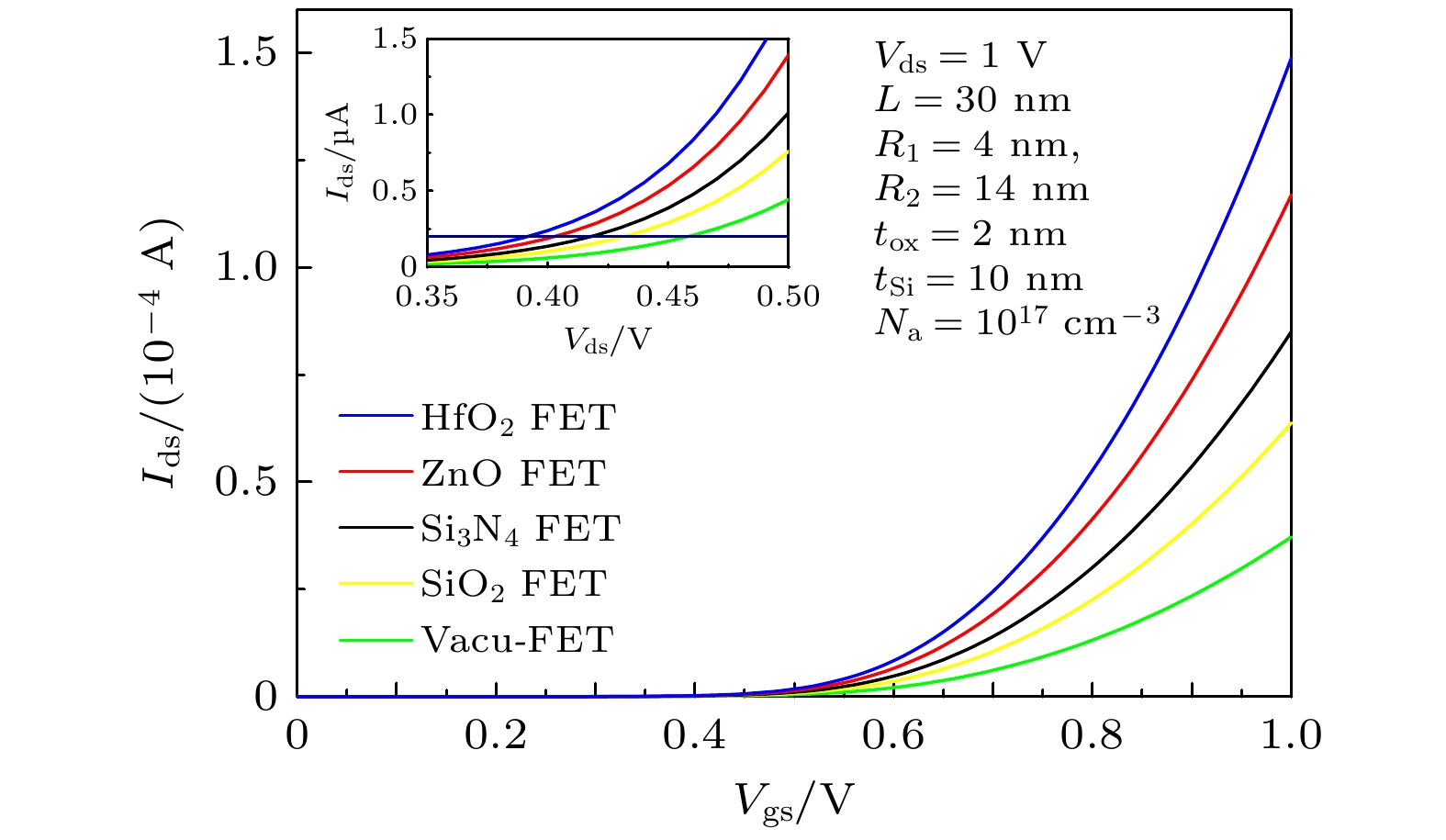
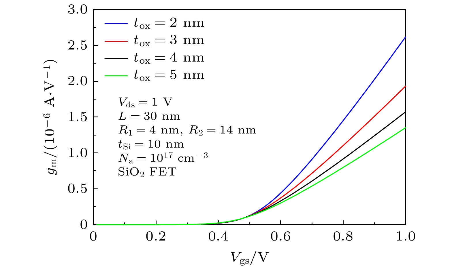
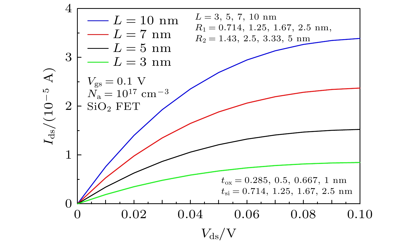
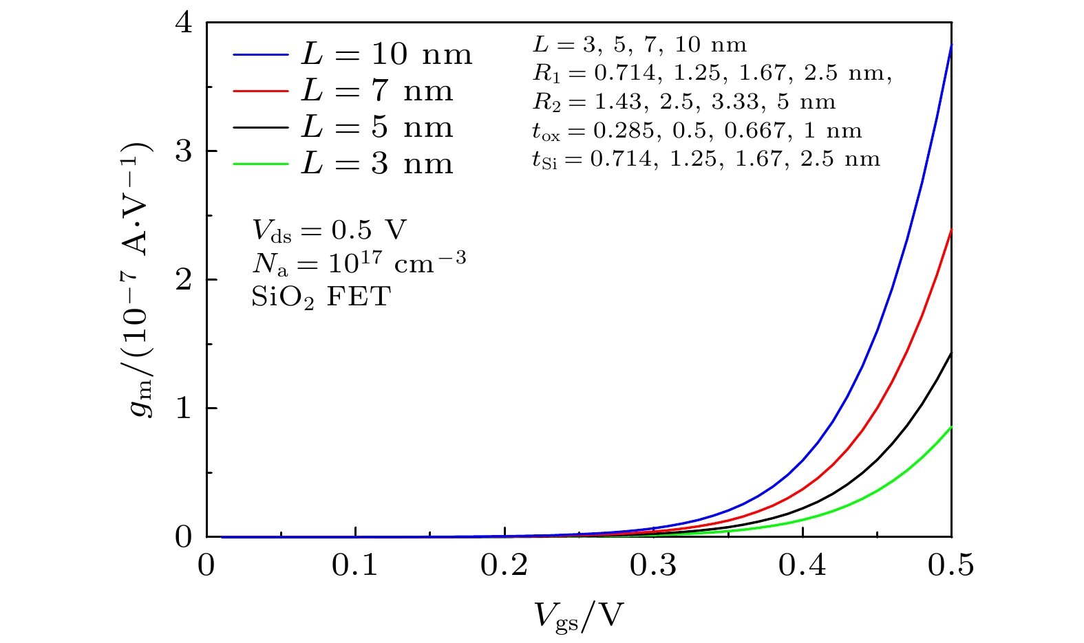
圆柱形双栅场效应晶体管(CSDG MOSFET)是在围栅MOSFET器件增加内部控制栅而形成, 与双栅、三栅及围栅MOSFET器件相比, 圆柱形双栅MOSFET提供了更好的栅控性能和输出特性. 本文通过求解圆柱坐标系下的二维泊松方程, 得到了圆柱形双栅 MOSFET的电势模型; 进一步对反型电荷沿沟道积分, 建立其漏源电流模型. 分析讨论了圆柱形双栅MOSFET器件的电学特性, 结果表明: 圆柱形双栅MOSFET外栅沿沟道的最小表面势和器件的阈值电压随栅介质层介电常数的增大而减小, 其漏源电流和跨导随栅介质层介电常数的增大而增大; 随着器件参数的等比例缩小, 沟道反型电荷密度减小, 其漏源电流和跨导也减小.
-
关键词:
- 圆柱形双栅场效应晶体管 /
- 模型 /
- 栅介质 /
- 电学特性
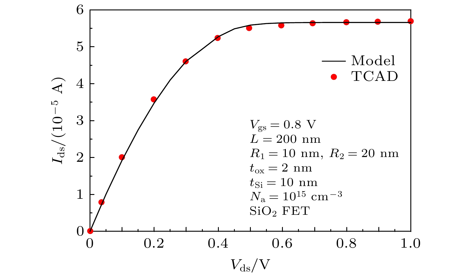
The cylindrical surrounding double-gate metal-oxide-semiconductor field-effect transistor (CSDG MOSFET) is formed by adding an internal control gate to the cylindrical surrounding-gate (CSG) MOSFET. The inner gate of CSDG MOSFET acts as a second gate for enhanced charge control. At present, the research of CSDG MOSFET structure is widely concerned. Compared with double-gate MOSFET, triple-gate MOSFET and CSG MOSFET, the CSDG MOSFET provides good controllability of the gate over the channel. Additionally, the device allows for higher volume inversion than CSG MOSFET, which leads to better output characteristics. In order to study the electrical characteristics of CSDG MOSFET, the potential model of CSDG MOSFET is obtained by solving the two-dimensional Poisson equation in cylindrical coordinates. The effects of gate dielectric, channel length and gate dielectric thickness on the surface potential and electric field of CSDG MOSFET are studied. Besides, the drain-source current model of CSDG MOSFET is established by integrating the inverse charge along the channel. The effects of gate dielectric and gate dielectric thickness on the transconductance of CSDG MOSFET are studied. In addition, the effects of the downscaling of device parameters on the transfer characteristics and transconductance of CSDG MOSFET are studied. The electrical characteristics of CSDG MOSFET are analyzed and discussed. The results show that the minimum surface potential along the channel of CSDG MOSFET decreases with the increase of gate dielectric constant of gate dielectric layer. The electric field along the channel and along the radius, drain-source current and transconductance of CSDG MOSFET increase as the gate dielectric constant increases. The threshold voltage of CSDG MOSFET decreases as the gate dielectric constant increases. Moreover, with the downscaling of device parameters, the transfer characteristics and transconductance of CSDG MOSFET decrease. The performance of CSDG MOSFET can be significantly improved by using high-k gate dielectrics. -
Keywords:
- cylindrical surrounding double-gate metal-oxide-semiconductor field-effect transistor /
- model /
- gate dielectric /
- electrical characteristics
[1] Kumar S, Goel E, Singh K, Singh B, Kumar M, Jit S 2016 IEEE Trans. Electron Dev. 63 3291
 Google Scholar
[2] Trevisoli R D, Doria R T, Souza M D, Das S, Ferain I, Pavanello M A 2012 IEEE Trans. Electron Dev. 59 3510
 Google Scholar
[3] Xiao Y, Zhang B, Lou H, Zhang L, Lin X 2016 IEEE Trans. Electron Dev. 63 2176
 Google Scholar
[4] Fahad H M, Smith C E, Rojas J P, Hussain M M 2011 Nano Lett. 11 4393
 Google Scholar
[5] Tekleab D 2014 IEEE Electr. Device Lett. 35 506
 Google Scholar
[6] Maduagwu U A, Srivastava V M 2020 IEEE Access 8 121204
 Google Scholar
[7] Oyedeji O E, Srivastava V M 2019 IEEE Conference on Information and Communication Technology Allahabad, India, December 6−8, 2019 p1−5
[8] Oyedeji O E, Srivastava V M 2019 10 th International Conference on Computing, Communication and Networking Technologies (ICCCNT) Kanpur, India, July 6−8, 2019 p1
[9] Shunqukela M, Srivastava V M 2018 International Conference on Computer Communication and Informatics (ICCCI) Coimbatore, India, January 4−6, 2018 p1
[10] Fahad H M, Hussain M M 2012 Sci. Rep. 2 475
 Google Scholar
[11] Verma J, Pratap Y, Gupta M, Haldar S, Gupta R S 2015 Annual IEEE India Conference (INDICON) New Delhi, India, December 17−20, 2015 p1
[12] Bairagya S, Chakraborty A 2017 Devices for Integrated Circuit (DevIC) Kalyani, India, March 23−24, 2017 p721−725
[13] Maduagwu U A, Srivastava V M 2019 J. Low Power Electron. Appl. 9 10
 Google Scholar
[14] Balestra F, Cristoloveanu S, Benachir M, Brini J, Elewa T 1987 IEEE Electr. Device Lett. 8 410
 Google Scholar
[15] Kloes A, Schwarz M, Holtij T, Navas A 2013 IEEE Trans. Electron Dev. 60 2691
 Google Scholar
[16] Pandian M K, Balamurugan N B 2014 J. Electr. Eng. Technol. 9 2079
 Google Scholar
[17] Bland D R 1961 Solutions of Laplace’s Equation (New York: Springer Netherlands) pp15−28
[18] Jimenez D, Saenz J J, Iniguez B, Sune J, Pallares J 2004 IEEE Electr. Device Lett. 25 314
 Google Scholar
[19] Li C, Zhuang Y, Di S, Han R 2013 IEEE Trans. Electron Dev. 60 3655
 Google Scholar
[20] Chen Q, Agrawal B, Meindl J D 2002 IEEE Trans. Electron Dev. 49 1086
 Google Scholar
[21] Lin S H, Zhou X, See G H, Zhu Z M, Lim G H, Wei C Q, Zhu G J, Yao Z H, Wang X F, Yee M 2007 IEEE Conference on Nanotechnology (IEEE NANO) Hong Kong, China, August 2−5, 2007 p889
[22] Ortiz-Conde A, Sanchez F J G, Guzman M 2003 Solid-State Electron. 47 2067
 Google Scholar
[23] Verma J, Haldar S, Gupta R S, Gupta M J S 2015 Superlattices Microst. 88 354
 Google Scholar
[24] Rewari S, Haldar S, Nath V, Deswal S S, Gupta R S 2016 Superlattices Microst. 90 8
 Google Scholar
[25] Sarkar C K 2016 Technology Computer Aided Design: Simulation for VLSI MOSFET (Boca Raton: CRC Press) pp273−288
[26] Kumar A, Bhushan S, Tiwari P K 2019 IET Circ. Devices Syst. 13 519
 Google Scholar
-
表 1 CSDG MOSFET器件参数值
Table 1. Model parameters of CSDG MOSFET.
参数 定义 数值 R1/nm 内栅介质层与硅体
接触处半径4 R2/nm 外栅介质层与硅体
接触处半径14 L/nm 栅长度 30 tox/nm 介质层厚度 2 Na/cm–3 沟道掺杂浓度 1017 ε0/(F·cm–1) 真空介电常数 8.854 × 10⁻¹⁴ εox 栅介质介电常数 ε0, 3.9ε0, 7ε0, 12ε0, 20ε0 εsi 硅介电常数 11.8ε0 表 2 不同栅长的CSDG MOSFET器件参数值
Table 2. Model parameters of CSDG MOSFET with different gate length.
L/nm R1/nm R2/nm tox/nm tSi/nm 3 0.714 1.43 0.285 0.714 5 1.25 2.5 0.5 1.25 7 1.67 3.33 0.667 1.67 10 2.5 5 1 2.5 -
[1] Kumar S, Goel E, Singh K, Singh B, Kumar M, Jit S 2016 IEEE Trans. Electron Dev. 63 3291
 Google Scholar
[2] Trevisoli R D, Doria R T, Souza M D, Das S, Ferain I, Pavanello M A 2012 IEEE Trans. Electron Dev. 59 3510
 Google Scholar
[3] Xiao Y, Zhang B, Lou H, Zhang L, Lin X 2016 IEEE Trans. Electron Dev. 63 2176
 Google Scholar
[4] Fahad H M, Smith C E, Rojas J P, Hussain M M 2011 Nano Lett. 11 4393
 Google Scholar
[5] Tekleab D 2014 IEEE Electr. Device Lett. 35 506
 Google Scholar
[6] Maduagwu U A, Srivastava V M 2020 IEEE Access 8 121204
 Google Scholar
[7] Oyedeji O E, Srivastava V M 2019 IEEE Conference on Information and Communication Technology Allahabad, India, December 6−8, 2019 p1−5
[8] Oyedeji O E, Srivastava V M 2019 10 th International Conference on Computing, Communication and Networking Technologies (ICCCNT) Kanpur, India, July 6−8, 2019 p1
[9] Shunqukela M, Srivastava V M 2018 International Conference on Computer Communication and Informatics (ICCCI) Coimbatore, India, January 4−6, 2018 p1
[10] Fahad H M, Hussain M M 2012 Sci. Rep. 2 475
 Google Scholar
[11] Verma J, Pratap Y, Gupta M, Haldar S, Gupta R S 2015 Annual IEEE India Conference (INDICON) New Delhi, India, December 17−20, 2015 p1
[12] Bairagya S, Chakraborty A 2017 Devices for Integrated Circuit (DevIC) Kalyani, India, March 23−24, 2017 p721−725
[13] Maduagwu U A, Srivastava V M 2019 J. Low Power Electron. Appl. 9 10
 Google Scholar
[14] Balestra F, Cristoloveanu S, Benachir M, Brini J, Elewa T 1987 IEEE Electr. Device Lett. 8 410
 Google Scholar
[15] Kloes A, Schwarz M, Holtij T, Navas A 2013 IEEE Trans. Electron Dev. 60 2691
 Google Scholar
[16] Pandian M K, Balamurugan N B 2014 J. Electr. Eng. Technol. 9 2079
 Google Scholar
[17] Bland D R 1961 Solutions of Laplace’s Equation (New York: Springer Netherlands) pp15−28
[18] Jimenez D, Saenz J J, Iniguez B, Sune J, Pallares J 2004 IEEE Electr. Device Lett. 25 314
 Google Scholar
[19] Li C, Zhuang Y, Di S, Han R 2013 IEEE Trans. Electron Dev. 60 3655
 Google Scholar
[20] Chen Q, Agrawal B, Meindl J D 2002 IEEE Trans. Electron Dev. 49 1086
 Google Scholar
[21] Lin S H, Zhou X, See G H, Zhu Z M, Lim G H, Wei C Q, Zhu G J, Yao Z H, Wang X F, Yee M 2007 IEEE Conference on Nanotechnology (IEEE NANO) Hong Kong, China, August 2−5, 2007 p889
[22] Ortiz-Conde A, Sanchez F J G, Guzman M 2003 Solid-State Electron. 47 2067
 Google Scholar
[23] Verma J, Haldar S, Gupta R S, Gupta M J S 2015 Superlattices Microst. 88 354
 Google Scholar
[24] Rewari S, Haldar S, Nath V, Deswal S S, Gupta R S 2016 Superlattices Microst. 90 8
 Google Scholar
[25] Sarkar C K 2016 Technology Computer Aided Design: Simulation for VLSI MOSFET (Boca Raton: CRC Press) pp273−288
[26] Kumar A, Bhushan S, Tiwari P K 2019 IET Circ. Devices Syst. 13 519
 Google Scholar
计量
- 文章访问数: 7973
- PDF下载量: 147
- 被引次数: 0


 下载:
下载:
