


-
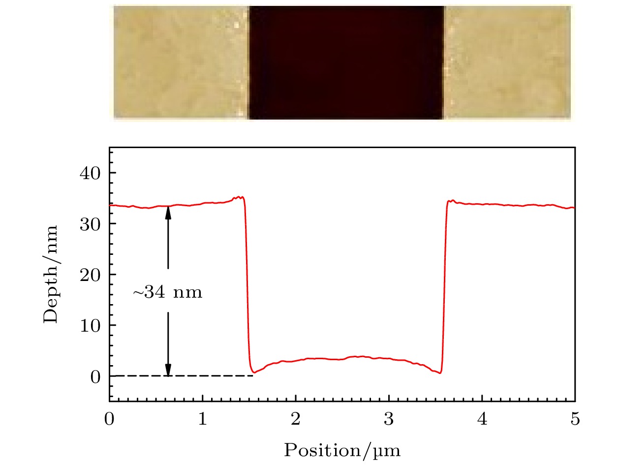
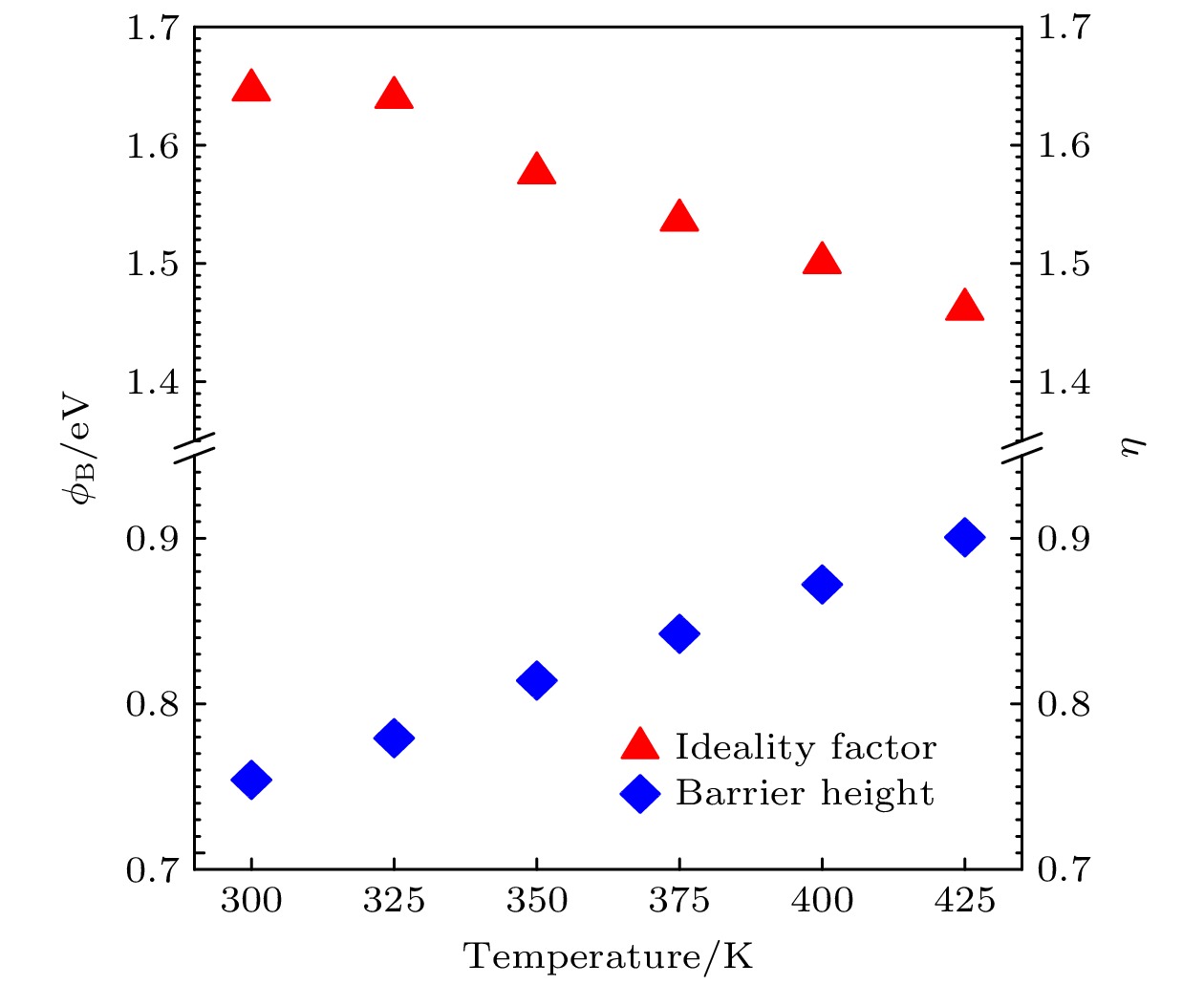
氮化镓材料具有大的禁带宽度(3.4 eV)、高的击穿场强(3.3 MV/cm), 在高温、高压等方面有良好的应用前景. 尤其是对于铝镓氮/氮化镓异质结构材料而言, 由极化效应产生的高面密度和高迁移率二维电子气在降低器件导通电阻、提高器件工作效率方面具有极大的优势. 由于缺乏高质量、大尺寸的氮化镓单晶衬底, 常规氮化镓材料均是在蓝宝石、硅和碳化硅等异质衬底上外延而成. 较大的晶格失配和热失配导致异质外延过程中产生密度高达107—1010 cm–2的穿透位错, 使器件性能难以进一步提升. 本文采用基于自支撑氮化镓衬底的铝镓氮/氮化镓异质结构材料制备凹槽阳极结构肖特基势垒二极管, 通过对欧姆接触区域铝镓氮势垒层刻蚀深度的精确控制, 依托单步自对准凹槽欧姆接触技术解决了低位错密度自支撑氮化镓材料的低阻欧姆接触技术难题, 实现了接触电阻仅为0.37 Ω·mm的低阻欧姆接触; 通过采用慢速低损伤刻蚀技术制备阳极凹槽区域, 使器件阳极金属与氮化镓导电沟道直接接触, 实现了高达3 × 10⁷开关比的高性能器件, 且器件开启电压仅为0.67 V, 425 K高温下, 器件反向漏电仅为1.6 × 10⁻⁷ A/mm. 实验结果表明, 基于自支撑氮化镓衬底的凹槽阳极结构铝镓氮/氮化镓肖特基势垒二极管可以有效抑制器件反向漏电, 极大地提升器件电学性能.Benefiting from the excellent properties of GaN with a wide bandgap of 3.4 eV as well as high critical field of 3.3 MV/cm, GaN-based devices prove to be a promising candidate in extreme conditions. Especially, high-density high-mobility two-dimensional electron gas (2DEG) induced by spontaneous piezoelectric polarization in AlGaN/GaN heterostructure enables AlGaN/GaN device to lower on-resistance (RON). However, owing to the lack of free-standing GaN substrate with large size and high quality, the epitaxis of GaN is always based on hetero-substrate such as Al2O3, Si and SiC, which shows large lattice mismatch and thermal mismatch. The large mismatch between GaN and substrate leads to high dislocation as well as high leakage current (IR) of GaN devices. In this work, high-performance AlGaN/GaN Schottky barrier diode with low IR and low turn-on voltage (VON) is fabricated on a 3-inch free-standing GaN substrate with C-doping GaN buffer layer to suppress IR. Owing to the suppressed dislocation density of the AlGaN/GaN epitaxial wafer on free-standing substrate, low Ohmic contact resistance (RC) is difficult to achieve the suppressed penetration of Ohmic metal into 2DEG channel, which is adverse to the high current density. In this work, a low RC of 0.37 Ω·mm is obtained by one-step self-aligned Ohmic process, including the etching of partial AlGaN barrier layer and lift-off of Ohmic metal. The 2DEG is formed under the effect of residual AlGaN barrier layer, and the short distance between 2DEG and Ohmic metal contributes to lowering the value of RC. The groove anode region is defined by the low damaged inductively coupled plasma process with a low etching rate of 1 nm/min, and the total depth is 35 nm, confirmed by atomic force microscope. Fully removing the AlGaN barrier layer from the anode region makes the anode metal directly contact the 2DEG channel, thereby improving the performance of the fabricated AlGaN/GaN Schottky barrier diode (SBD) with a low VON of 0.67 V, low IR of 3.6 × 10⁻⁸ A/mm, and an ION/IOFF ratio of up to 3 × 10⁷. The values of differential RON,sp are calculated to be 0.44, 0.86, 1.59, 2.55 mΩ·cm2 for GaN SBDs with various values of LAC of 6, 10, 15, 20 μm, and the values of RON,sp determined at an anode current density of 100 mA/mm are 1.27, 2.08, 3.29, 4.63 mΩ·cm2, respectively. As the measured temperature increases from 300 to 425 K, the IR is increased only by 3 times to 1.6 × 10⁻⁷ A/mm, which shows the great potential for next-generation power electronics.
[1] Zhang T, Wang Y, Zhang Y N, Lv Y G, Ning J, Zhang Y C, Zhou H, Duan X L, Zhang J C, Hao Y 2021 IEEE Trans. Electron Devices 68 2661
 Google Scholar
[2] Hao R H, Li W Y, Fu K, Yu G H, Song L, Yuan J, Li J S, Deng X G, Zhang X D, Zhou Q, Fan Y M, Shi W H, Cai Y, Zhang X P, Zhang B S 2017 IEEE Electron Device Lett. 38 1567
Google Scholar
[3] Zhang L, Zheng Z Y, Yang S, Song W J, He J B, Chen K J 2021 IEEE Electron Device Lett. 42 22
Google Scholar
[4] Zhang T, Li R H, Lu J, Zhang Y N, Lv Y G, Duan X L, Xu S R, Zhang J C, Hao Y 2021 IEEE Electron Device Lett. 42 1747
Google Scholar
[5] Hsin Y M, Ke T Y, Lee G Y, Chyi J I, Chiu H C 2012 Phys. Status Solidi C 9 949
Google Scholar
[6] Nela L, Erp R V, Kampitsis G, Yildirim H K, Ma J, Matioli E 2021 IEEE Trans. Power Electron. 36 1269
Google Scholar
[7] Tsou C W, Wei K P, Lian Y W, Hsu S S H 2016 IEEE Electron Device Lett. 37 70
Google Scholar
[8] Gao J N, Wang M J, Yin R Y, Liu S F, Wen C P, Wang J Y, Wu W G, Hao Y L, Jin Y F, Shen B 2017 IEEE Electron Device Lett. 38 1425
Google Scholar
[9] Hu J, Stoffels S, Lenci S, Bakeroot B, Jaeger B D, Hove M V, Ronchi N, Venegas R, Liang H, Zhao M, Groeseneken G, Decoutere S 2016 IEEE Trans. Electron Devices 63 997
Google Scholar
[10] Li X D, Hove M V, Zhao M, Geens K, Lempinen V P, Sormunen J, Groeseneken G, Decoutere S 2017 IEEE Electron Device Lett. 38 918
Google Scholar
[11] Ma J, Matioli E 2018 Appl. Phys. Lett. 112 052101
Google Scholar
[12] Zhang T, Lv Y G, Li R H, Zhang Y N, Zhang Y C, Li X D, Zhang J C, Hao Y 2021 IEEE Electron Device Lett. 42 477
Google Scholar
[13] Zhou Q, Jin Y, Shi Y Y, Mou J Y, Bao X, Chen B W, Zhang B 2015 IEEE Electron Device Lett. 36 660
Google Scholar
[14] Bahat-Treidel E, Hilt O, Zhytnytska R, Wentzel A, Meliani C, Wurfl J, Trankle G 2012 IEEE Electron Device Lett. 33 357
Google Scholar
[15] Lee J G, Park B R, Cho C H, Seo K S, Cha H Y 2013 IEEE Electron Device Lett. 34 214
Google Scholar
[16] Xiao M, Ma Y W, Cheng K, Liu K, Xie A, Beam E, Cao Y, Zhang Y H 2020 IEEE Electron Device Lett. 41 1177
Google Scholar
[17] Wang T T, Wang X, He Y, Jia M, Ye Q, Xu Y, Zhang Y H, Li Y, Bai L H, Ma X H, Hao Y 2021 IEEE Trans. Electron Devices 68 2867
Google Scholar
[18] Ma J, Santoruvo G, Tandon P, Matioli E 2016 IEEE Trans. Electron Devices 63 3614
Google Scholar
[19] Gao J N, Jin Y F, Xie B, Wen C P, Hao Y L, Shen B, Wang M J 2018 IEEE Electron Device Lett. 39 859
Google Scholar
[20] Zhang T, Zhang Y N, Zhang J C, Li X D, Lv Y G, Hao Y 2021 IEEE Electron Device Lett. 42 304
Google Scholar
[21] Fu H Q, Fu K, Alugubelli S R, Cheng C Y, Huang X Q, Chen H, Yang T H, Yang C, Zhou J G, Montes J, Deng X G, Qi X, Goodnick S M, Ponce F A, Zhao Y J 2020 IEEE Electron Device Lett. 41 127
Google Scholar
[22] Kizilyalli I C, Edwards A P, Nie H, Disney D, Bour D 2013 IEEE Trans. Electron Devices 60 3067
Google Scholar
[23] Lin W, Wang M J, Yin R Y, Wei J, Wen C P, Xie B, Hao Y L, Shen B 2021 IEEE Electron Device Lett. 42 1124
Google Scholar
[24] Liu X K, Gu H, Li K L, Guo L C, Zhu D L, Lu Y M, Wang J F, Kuo H C, Liu Z H, Liu W J, Chen L, Fang J P, Ang K W, Xu K, Ao J P 2017 AIP Adv. 7 095305
Google Scholar
[25] Chu J Y, Wang Q, Jiang L J, Feng C, Li W, Liu H X, Xiao H L, Wang X L 2021 J. Electron Mater. 50 2630
Google Scholar
[26] Alshahed M, Heuken L, Alomari M, Cora I, Toth L, Pecz B, Wachter C, Bergunde T, Burghartz J N 2018 IEEE Trans. Electron Devices 65 2939
Google Scholar
[27] Gao J N, Jin Y F, Hao Y L, Xie B, Wen C P, Shen B, Wang M J 2018 IEEE Trans. Electron Devices 65 1728
Google Scholar
[28] Wu J Y, Lei S Q, Cheng W C, Sokolovskij R, Wang Q, Xia G R, Yu H Y 2019 J. Vac. Sci. Technol. A 37 060401
Google Scholar
[29] Zhang T, Zhang J C, Zhou H, Chen T S, Zhang K, Hu Z Z, Bian Z K, Dang K, Wang Y, Zhang L, Ning J, Ma P J, Hao Y 2018 IEEE Electron Device Lett. 39 1548
Google Scholar
[30] Zhu M D, Song B, Qi M, Hu Z Y, Nomoto K, Yan X D, Cao Y, Johnson W, Kohn E, Jena D, Xing H G 2015 IEEE Electron Device Lett. 36 375
Google Scholar
[31] Chen J B, Bian Z K, Liu Z H, Zhu D, Duan X L, Wu Y H, Jia Y Q, Ning J, Zhang J C, Hao Y 2021 J. Alloys Compd. 853 156978
Google Scholar
[32] Toumi S, Ferhat-Hamida A, Boussouar L, Sellai A, Ouennoughi A, Ryssel H, 2009 Microelectron. Eng. 86 303
Google Scholar
-
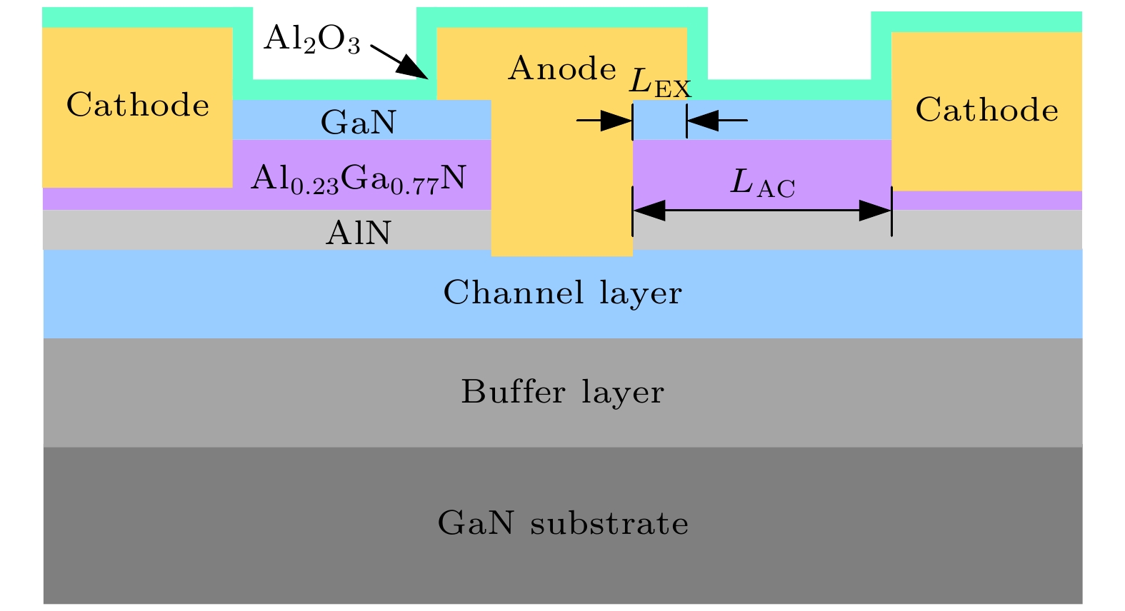
图 1 自支撑衬底凹槽阳极结构AlGaN/GaN SBD器件截面图
Fig. 1. Schematic cross-sectional of AlGaN/GaN SBD with groove anode on free-standing GaN substrate.
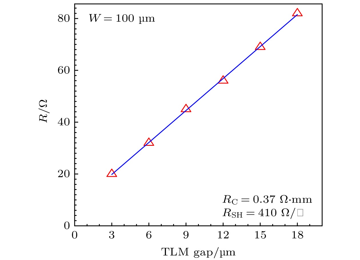
图 3 测试电阻与传输线模型电极间距的线性拟合
Fig. 3. Linear fitting of the measured resistance versus the TLM metal pad gap.
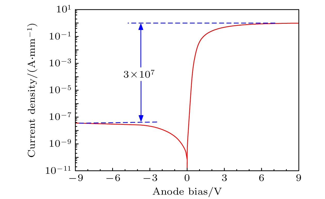
图 4 自支撑氮化镓衬底凹槽阳极结构AlGaN/GaN SBD的正反向I-V曲线
Fig. 4. Forward and reverse I-V curve of the fabricated AlGaN/GaN SBD with groove anode on free-standing GaN substrate.
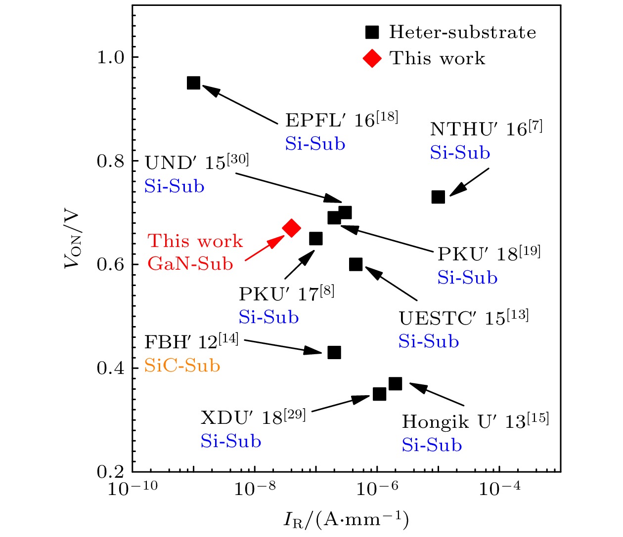
图 5 不同衬底结构AlGaN/GaN SBD开启电压与反向漏电的对应关系
Fig. 5. Benchmarking the turn-on voltage and reverse current of AlGaN/GaN SBDs with various substrate.
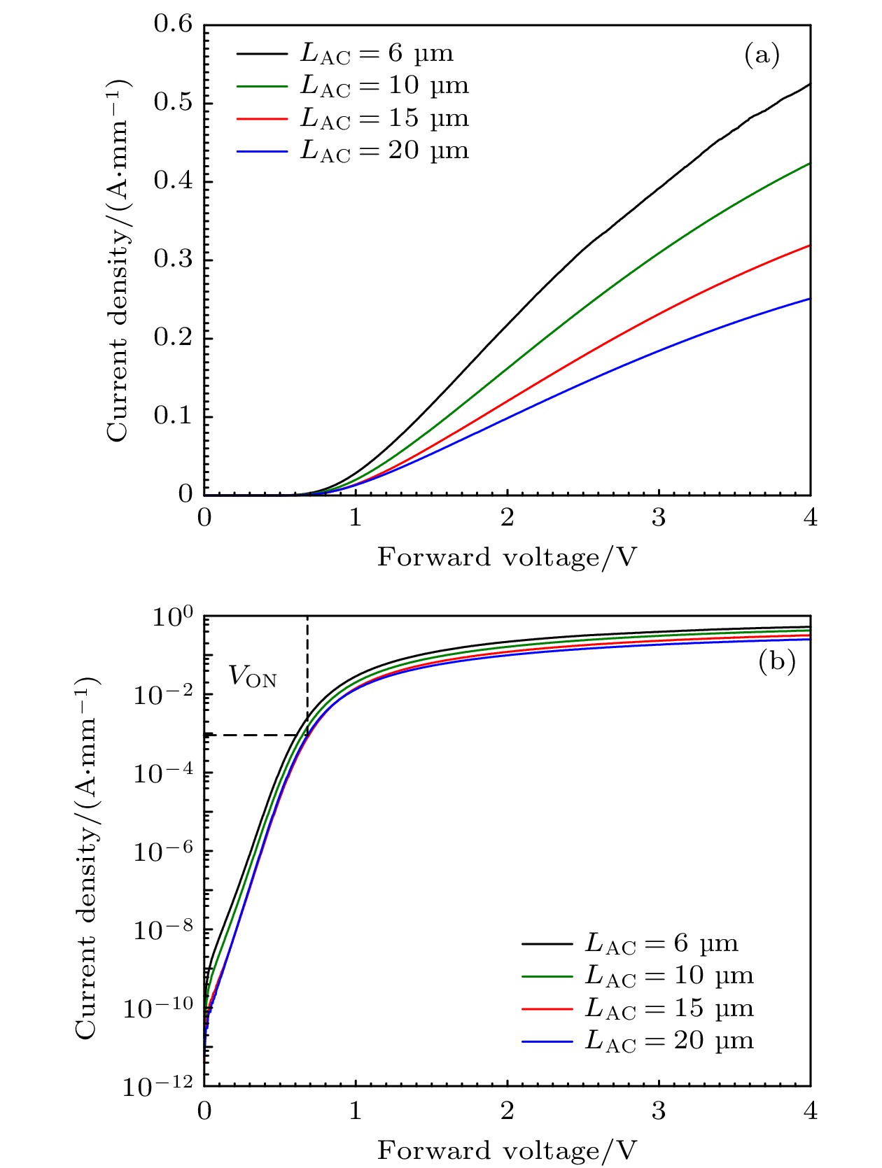
图 6 (a)线性坐标和(b)对数坐标下不同阴阳极间距AlGaN/GaN SBDs正向I-V特性
Fig. 6. Forward I-V characteristics of the fabricated AlGaN/GaN SBDs with various LAC in (a) linear-scale and (b) semi-log scale.
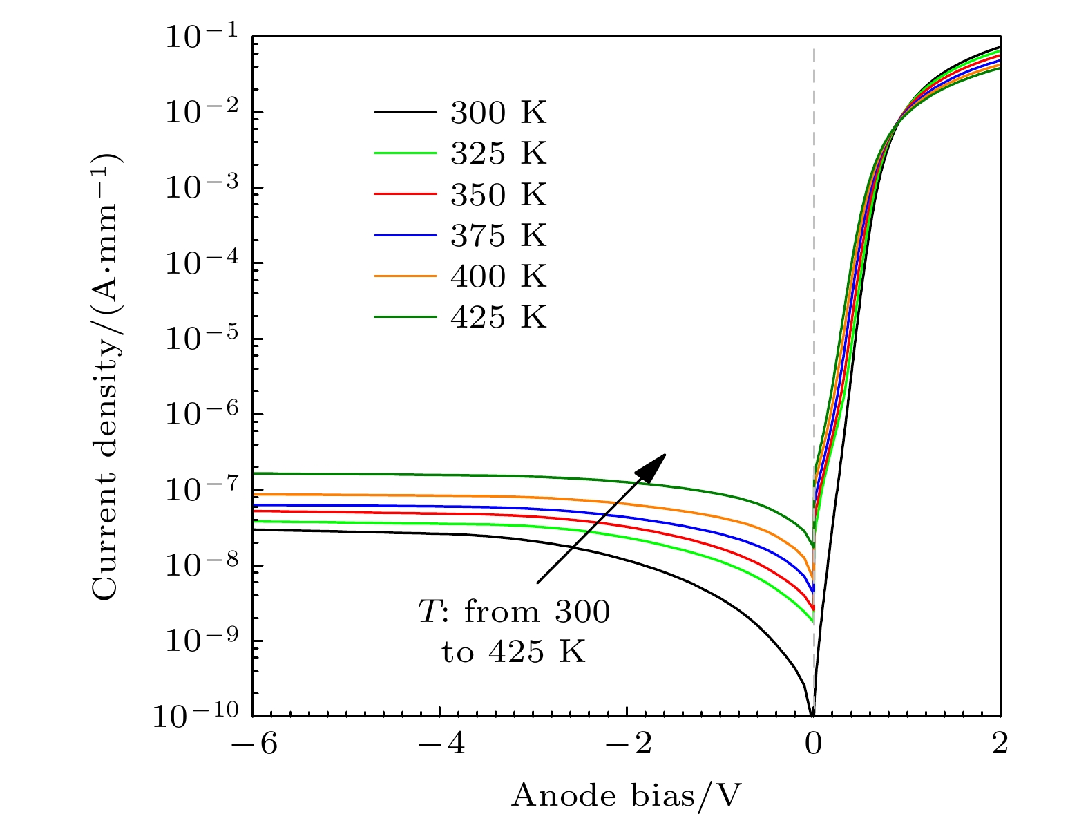
图 7 半对数坐标下自支撑氮化镓衬底AGaN/GaN SBD正反向I-V特性随温度的变化关系
Fig. 7. Temperature-dependent forward and reverse I-V characteristics of AlGaN/GaN SBD on free-standing GaN substrate in semi-log scale.
-
[1] Zhang T, Wang Y, Zhang Y N, Lv Y G, Ning J, Zhang Y C, Zhou H, Duan X L, Zhang J C, Hao Y 2021 IEEE Trans. Electron Devices 68 2661
Google Scholar
[2] Hao R H, Li W Y, Fu K, Yu G H, Song L, Yuan J, Li J S, Deng X G, Zhang X D, Zhou Q, Fan Y M, Shi W H, Cai Y, Zhang X P, Zhang B S 2017 IEEE Electron Device Lett. 38 1567
Google Scholar
[3] Zhang L, Zheng Z Y, Yang S, Song W J, He J B, Chen K J 2021 IEEE Electron Device Lett. 42 22
Google Scholar
[4] Zhang T, Li R H, Lu J, Zhang Y N, Lv Y G, Duan X L, Xu S R, Zhang J C, Hao Y 2021 IEEE Electron Device Lett. 42 1747
Google Scholar
[5] Hsin Y M, Ke T Y, Lee G Y, Chyi J I, Chiu H C 2012 Phys. Status Solidi C 9 949
Google Scholar
[6] Nela L, Erp R V, Kampitsis G, Yildirim H K, Ma J, Matioli E 2021 IEEE Trans. Power Electron. 36 1269
Google Scholar
[7] Tsou C W, Wei K P, Lian Y W, Hsu S S H 2016 IEEE Electron Device Lett. 37 70
Google Scholar
[8] Gao J N, Wang M J, Yin R Y, Liu S F, Wen C P, Wang J Y, Wu W G, Hao Y L, Jin Y F, Shen B 2017 IEEE Electron Device Lett. 38 1425
Google Scholar
[9] Hu J, Stoffels S, Lenci S, Bakeroot B, Jaeger B D, Hove M V, Ronchi N, Venegas R, Liang H, Zhao M, Groeseneken G, Decoutere S 2016 IEEE Trans. Electron Devices 63 997
Google Scholar
[10] Li X D, Hove M V, Zhao M, Geens K, Lempinen V P, Sormunen J, Groeseneken G, Decoutere S 2017 IEEE Electron Device Lett. 38 918
Google Scholar
[11] Ma J, Matioli E 2018 Appl. Phys. Lett. 112 052101
Google Scholar
[12] Zhang T, Lv Y G, Li R H, Zhang Y N, Zhang Y C, Li X D, Zhang J C, Hao Y 2021 IEEE Electron Device Lett. 42 477
Google Scholar
[13] Zhou Q, Jin Y, Shi Y Y, Mou J Y, Bao X, Chen B W, Zhang B 2015 IEEE Electron Device Lett. 36 660
Google Scholar
[14] Bahat-Treidel E, Hilt O, Zhytnytska R, Wentzel A, Meliani C, Wurfl J, Trankle G 2012 IEEE Electron Device Lett. 33 357
Google Scholar
[15] Lee J G, Park B R, Cho C H, Seo K S, Cha H Y 2013 IEEE Electron Device Lett. 34 214
Google Scholar
[16] Xiao M, Ma Y W, Cheng K, Liu K, Xie A, Beam E, Cao Y, Zhang Y H 2020 IEEE Electron Device Lett. 41 1177
Google Scholar
[17] Wang T T, Wang X, He Y, Jia M, Ye Q, Xu Y, Zhang Y H, Li Y, Bai L H, Ma X H, Hao Y 2021 IEEE Trans. Electron Devices 68 2867
Google Scholar
[18] Ma J, Santoruvo G, Tandon P, Matioli E 2016 IEEE Trans. Electron Devices 63 3614
Google Scholar
[19] Gao J N, Jin Y F, Xie B, Wen C P, Hao Y L, Shen B, Wang M J 2018 IEEE Electron Device Lett. 39 859
Google Scholar
[20] Zhang T, Zhang Y N, Zhang J C, Li X D, Lv Y G, Hao Y 2021 IEEE Electron Device Lett. 42 304
Google Scholar
[21] Fu H Q, Fu K, Alugubelli S R, Cheng C Y, Huang X Q, Chen H, Yang T H, Yang C, Zhou J G, Montes J, Deng X G, Qi X, Goodnick S M, Ponce F A, Zhao Y J 2020 IEEE Electron Device Lett. 41 127
Google Scholar
[22] Kizilyalli I C, Edwards A P, Nie H, Disney D, Bour D 2013 IEEE Trans. Electron Devices 60 3067
Google Scholar
[23] Lin W, Wang M J, Yin R Y, Wei J, Wen C P, Xie B, Hao Y L, Shen B 2021 IEEE Electron Device Lett. 42 1124
Google Scholar
[24] Liu X K, Gu H, Li K L, Guo L C, Zhu D L, Lu Y M, Wang J F, Kuo H C, Liu Z H, Liu W J, Chen L, Fang J P, Ang K W, Xu K, Ao J P 2017 AIP Adv. 7 095305
Google Scholar
[25] Chu J Y, Wang Q, Jiang L J, Feng C, Li W, Liu H X, Xiao H L, Wang X L 2021 J. Electron Mater. 50 2630
Google Scholar
[26] Alshahed M, Heuken L, Alomari M, Cora I, Toth L, Pecz B, Wachter C, Bergunde T, Burghartz J N 2018 IEEE Trans. Electron Devices 65 2939
Google Scholar
[27] Gao J N, Jin Y F, Hao Y L, Xie B, Wen C P, Shen B, Wang M J 2018 IEEE Trans. Electron Devices 65 1728
Google Scholar
[28] Wu J Y, Lei S Q, Cheng W C, Sokolovskij R, Wang Q, Xia G R, Yu H Y 2019 J. Vac. Sci. Technol. A 37 060401
Google Scholar
[29] Zhang T, Zhang J C, Zhou H, Chen T S, Zhang K, Hu Z Z, Bian Z K, Dang K, Wang Y, Zhang L, Ning J, Ma P J, Hao Y 2018 IEEE Electron Device Lett. 39 1548
Google Scholar
[30] Zhu M D, Song B, Qi M, Hu Z Y, Nomoto K, Yan X D, Cao Y, Johnson W, Kohn E, Jena D, Xing H G 2015 IEEE Electron Device Lett. 36 375
Google Scholar
[31] Chen J B, Bian Z K, Liu Z H, Zhu D, Duan X L, Wu Y H, Jia Y Q, Ning J, Zhang J C, Hao Y 2021 J. Alloys Compd. 853 156978
Google Scholar
[32] Toumi S, Ferhat-Hamida A, Boussouar L, Sellai A, Ouennoughi A, Ryssel H, 2009 Microelectron. Eng. 86 303
Google Scholar

 下载:
下载:
计量
- 文章访问数: 9407
- PDF下载量: 193
- 被引次数: 0
