


-
传统谐振式传感器的谐振敏感元件大多采用金属、石英晶体、硅等材料制成, 但随着谐振式传感器朝着小型化、微型化、实用化的趋势发展, 不但要求新型谐振子材料可进行微纳加工, 还对其灵敏度和精度提出了更高的要求. 石墨烯这种新型二维纳米材料, 因具有出色的力学、电学、光学、热学特性, 在谐振传感领域有着巨大的应用潜力和研究价值, 因此基于石墨烯材料的力学量传感器有望在小型化、高性能和环境适应性等多方面超越硅基力学量传感器. 本文针对石墨烯谐振式力学量传感器, 介绍了石墨烯材料的基本性质、制备与转移方法, 阐述了谐振式传感器的工作原理与应用特点, 进而分析了关于石墨烯谐振特性优化与谐振器制备的理论与实验研究; 在此基础上, 重点总结了石墨烯谐振器在压力、加速度、质量等传感器领域的研究进展, 梳理了石墨烯谐振式力学量传感器在薄膜转移、结构制备与激振/拾振等方面的技术问题, 同时也明确了石墨烯在谐振传感领域的研究价值和发展潜力.The resonant sensor is a kind of high-sensitivity and high-stability sensor that directly outputs digital signals. The resonance sensitive elements of traditional resonant sensors are mostly made of metal, quartz crystal, silicon and other materials. However, with the development of resonant sensor toward the miniaturization and intellectualization, the sensitive materials of new resonator are micro-nano machined and highly sensitive. As a new type of two-dimensional nanomaterial, graphene has the great potentials in the field of resonance sensing because of its excellent mechanical, electrical, optical and thermal properties. Therefore, the mechanical quantity sensor based on graphene material is expected to surpass the silicon material mechanical quantity sensor in many aspects such as micro-nano size, high performance, and environmental adaptability. This review focuses on the graphene resonant mechanical quantity sensor. In the first part, we summarize the basic properties, preparation methods, and transfer methods of graphene materials. The preparation and transmission methods of graphene are key to high-performance graphene resonator, but there are still different problems in the preparation and transfer of graphene, which also greatly restricts the development of graphene resonator. In the second part, the basic theory of resonant sensors is given, and the common methods of transferring graphene films are introduced in detail. Then the theoretical and experimental studies of graphene resonator are discussed. For example, the theoretical studies of graphene resonator are investigated by using the classical elastic theory, non-local elastic theory, molecular structure mechanics and molecular dynamics. Then the effects of graphene preparation method, graphene layer number and shape, excitation and detection methods on the resonance performance are estimated in the resonant experiments of graphene resonators. After that, the research progress of graphene resonator is summarized in the fields of pressure, acceleration and mass sensors. Compared with traditional silicon resonators, graphene resonators have a small dimension and demonstrate preferable resonant performance under low-temperature and low-pressure conditions. In this case, the technical issues of graphene resonant sensor are introduced to emphasize the importance of suspended graphene film transfer, structure fabrication of harmonic oscillator and vibration excitation/detection of resonators, which contributes to the potential applications in the fields of aerospace, intelligent detection and biomedical sensing for graphene resonant sensors.
-
Keywords:
- graphene /
- resonator /
- mechanical quantity sensor /
- performance analysis
[1] Tabata O, Yamamoto T 1999 Sensors and Actuators 75 53
 Google Scholar
[2] 樊尚春, 朱黎明, 邢维巍 2019 计测技术 39 4
Google Scholar
Fan S C, Zhu L M, Xing W W 2019 Metrology and Measurement Technology 39 4
Google Scholar
[3] Stachiv I, Gan L 2019 Materials 21 3593
Google Scholar
[4] Su S X P, Yang H S, Agino A M 2005 IEEE Sens. J. 5 1214
Google Scholar
[5] Nie J, Meng X, Li N, Lin L 2017 Sens. Actuat. B Chem. 256 1
Google Scholar
[6] Yu X, Chen X, Ding X, Zhao X 2017 IEEE Trans. Instrum. Meas. 67 1
Google Scholar
[7] Li C, Zhang Q W, Zhao Y L, Tian C, Li B, Han C, Bai B 2021 J. Micromech. Microeng. 31 115001
Google Scholar
[8] John G, Troy W 1993 Sens. Actuat. A Phys. 37 82
Google Scholar
[9] Ikeda K, Kuwayama H, Kobayashi T, Watanabe T, Nishikawa T, Yoshida T, Harada K 1990 Sens. Actuat. A Phys. 21 146
Google Scholar
[10] Chen F, Gao J, Tian W 2017 Sens. Actuat. A Phys. 269 427
Google Scholar
[11] Lei F, Dupuis P, Durrieu O, Zissis G, Maussion P 2017 IEEE Trans. Ind. Electron. 53 5988
Google Scholar
[12] 樊尚春, 孙苗苗, 李成 2012 传感技术学报 25 1
Google Scholar
Fan S C, Sun M M, Li C 2012 J. Trans. Technology 25 1
Google Scholar
[13] Novoselov K S, Geim A K, Morozov S V, Jiang D, Zhang Y, Dubonos S V, Grigorieva I V, Firsov A A 2004 Science 306 5696
Google Scholar
[14] Zhang Y B, Tan Y W, Stormer H L, Kim P 2005 Nature 438 201
Google Scholar
[15] Geim A K, Novoselov K S 2007 Nat. Mater. 6 183
Google Scholar
[16] Geim A K 2009 Science 324 1530
Google Scholar
[17] Rao C N, Sood A K, Subrahmanyam K S, Govindaraj A 2010 Angew. Chem. Int. Ed. Engl. 48 7752
Google Scholar
[18] Smith B R, Conger M J, Mcmullen J S, Neubert M J 2019 J. Bus. Ventur. Insights 11 1
Google Scholar
[19] Cabrera H, Mendoza D, Benítez J L, Bautista F C, Alvarado S, Marín E 2015 J. Phys. D: Appl. Phys. 48 465501
Google Scholar
[20] De S, Coleman J N 2010 Acs Nano. 4 2713
Google Scholar
[21] Nika D L, Askerov A S, Balandin A A 2012 Nano Lett. 12 3238
Google Scholar
[22] Pang C, Lee G Y, Kim T I, Sang M K, Hong N K, Ann S H, Sun K Y 2012 Nat. Mater. 11 795
Google Scholar
[23] Ding G, Li X, Xu Z, Chen H, Wang M 2021 IEEE Electr. Device Lett. 42 236
Google Scholar
[24] Jung M. W, Myung S, Kim K W, Song W, Jo Y Y, Lee S S, Lim J, Park C Y, An K S 2014 Nanotechnology 25 285302
Google Scholar
[25] Jaakkola K, Sandberg H, Lahti M, Ermolov V 2019 IEEE Trans. Compon. Pack. Manuf. Technol. 9 1
Google Scholar
[26] Lee H, Choi T K, Lee Y B, Cho H R, Ghaffari R, Wang L, Kim D H 2016 Nat. Nanotechnol. 11 566
Google Scholar
[27] Seo D H, Pineda S, Fang J, Gozukara Y, Yick S, Bendavid A. Lam S K H, Murdock A T, Murphy A B, Han Z J 2017 Nat. Commun. 8 14217
Google Scholar
[28] 黄乐, 张志勇, 彭练矛 2017 物理学报 66 218501
Google Scholar
Huang L, Zhang Z Y, Peng L M 2017 Acta Phys. Sin. 66 218501
Google Scholar
[29] 赵鹏程, 樊尚春 2017 计测技术 37 4
Google Scholar
Zhao P C, Fan S C 2017 Metro. Measure. Technol. 37 4
Google Scholar
[30] Stankovich S, Dikin D A, Piner R D, Kohlhaas K A, Kleinhammes A, Jia Y, Ruoff R S 2007 Carbon 45 1558
Google Scholar
[31] Ju H M, Huh S H, Choi S H, Lee H L 2010 Mater. Lett. 64 357
Google Scholar
[32] Wang H, Robinson J T, Li X, Dai H 2009 J. Am. Chem. Soc. 131 9910
Google Scholar
[33] Reina A, Jia X, Ho J, Nezich D, Son H, Bulovic V, Kong J 2009 Nano Lett. 9 3087
Google Scholar
[34] Li X, Cai W, An J, Kim S, Nah J, Yang D, Ruoff R S 2009 Science 324 1312
Google Scholar
[35] Sprinkle M, Ruan, Hu Y, Hankinson J, Rubio-Roy M, Zhang B, Wu X, Berger C, de Heer W A 2010 Nat. Nanotechnol. 5 727
Google Scholar
[36] Liang X, Sperling B A, Calizo I, Cheng G, Hacker C A, Zhang Q, Richter C A 2011 ACS Nano. 22 9144
Google Scholar
[37] Li X, Zhu Y, Cai W, Borysiak M, Han B, Chen D, Ruoff R S 2009 Nano Lett. 9 4359
Google Scholar
[38] Lee Y, Bae S, Jang H, Jang S, Zhu S E, Sim S H, Ahn J H 2010 Nano Lett. 10 490
Google Scholar
[39] Chandrashekar B N, Deng B, Smitha A S, Chen Y, Tan C, Zhang H, Liu Z F 2015 Adv. Mater. 27 5210
Google Scholar
[40] Kim K S, Zhao Y, Jang H, Lee S Y, Kim J M, Kim K S, Ahn J H, Kim P, Choi J Y, Hong B H 2009 Nature 457 706
Google Scholar
[41] Lin Y C, Jin C, Lee J C, Jen S F, Suenaga K, Chiu P W 2011 ACS Nano 5 2362
Google Scholar
[42] Lin Y C, Lu C C, Yeh C H, Jin C, Suenaga K, Chiu P W 2011 Nano Lett. 12 414
Google Scholar
[43] Bae S, Kim H, Lee Y, Xu X, Park J S, Zheng Y, Balakrishnan J, Lei T, Kim H R, Song Y I, Kim Y J, Kim K S, Ozyilmaz B, Ahn J H, Iijima S 2010 Nat. Nanotechnology 5 574
Google Scholar
[44] Kitipornchai S, He X Q, Liew K M 2005 Phys. Rev. B 72 075443
Google Scholar
[45] Sakhaee-Pour A, Ahmadian M T, Naghdabadi R 2008 Nanotechnology 19 085702
Google Scholar
[46] Atalaya J, Isacsson A, Kinaret J M 2008 Nano Lett. 8 4196
Google Scholar
[47] Murmu T, Pradhan S C 2009 J. Appl. Phys. 105 064319
Google Scholar
[48] Kwon O K, Lee G Y, Hwang H J, Kang J W 2012 Phys. E Low Dimens. Syst. Nanostruct. 45 194
Google Scholar
[49] Kwon O K, Lee J H, Park J, Kim K S, Kang J W 2013 Curr. Appl. Phys. B 13 360
Google Scholar
[50] Kang J W, Hwang H J, Kim K S 2012 Comput. Mater. Sci. 65 216
Google Scholar
[51] Kang J W, Kim H W, Kim K S, Lee J H 2013 Curr. Appl. Phys. 13 789
Google Scholar
[52] Young K S, Cho S Y, Won K J, Kuen K O 2013 Phys. E Low Dimens. Syst. Nanostruct. 54 118
Google Scholar
[53] Bunch J S, van der Zande A M, Verbridge S S, Frank I W, Tanenbaum D M, Parpia J M, McEuen P L 2007 Science 315 490
Google Scholar
[54] Garcia-Sanchez D, van der Zande A M, Paulo A S, Lassagne B, McEuen P L, Bachtold A 2008 Nano Lett. 8 1399
Google Scholar
[55] Kim S Y, Park H S 2009 Nano Lett. 9 969
Google Scholar
[56] Jiang J W, Wang J S 2012 J. Appl. Phys. 111 054314
Google Scholar
[57] Chen C, Rosenblatt S, Bolotin K I, Kalb W, Kim P, Kymissis I, Hone J 2009 Nat. Nanotechnol. 4 861
Google Scholar
[58] van der Zande A M, Barton R. A, Alden J S, Ruiz-Vargas C S, Whitney W S, Pham P H Q, McEuen P L 2010 Nano Lett. 10 4869
Google Scholar
[59] Guan F, Kumaravadivel P, Averin D V, Du X 2015 Appl. Phys. Lett. 107 193102
Google Scholar
[60] Barton R A, Ilic B, van der Zande A M, Whitney W S, McEuen P L, Parpia J M, Craighead H G 2011 Nano Lett. 11 1232
Google Scholar
[61] Oshidari Y, Hatakeyama T, Kometani R, Warisawa S, Ishihara S 2012 Appl. Phys. Express 5 117201
Google Scholar
[62] Lee S, Chen C, Deshpande V V, Lee G H, Lee I, Lekas M, Hone J 2013 Appl. Phys. Lett. 102 153101
Google Scholar
[63] Al-Mashaal A K, Wood G S, Torin A, Mastropaolo E, Newton M J, Cheung R 2018 IEEE Sens. J. 1 465
Google Scholar
[64] Miller D, Alemán B 2019 Appl. Phys. Lett. 115 193102
Google Scholar
[65] Bunch J S, Verbridge S S, Alden J S, van der Zande A M, Parpia J M, Craighead H G, McEuen P L 2008 Nano Lett. 8 2548
Google Scholar
[66] Ma J, Jin W, Xuan H, Wang C, Ho H L 2014 Opt. Lett. 39 4769
Google Scholar
[67] Dolleman R J, Davidovikj D, Cartamil-Bueno S J, van der Zant H S J, Steeneken P G 2016 Nano Lett. 16 568
Google Scholar
[68] Vollebregt S, Dolleman R J, van der Zant H S J, et al. 2017 19 th International Conference on Solid-State Sensors, Actuators and Microsystems (TRANSDUCERS) Kaohsiung, Taiwan, June 18–20, 2017 pp770–773
[69] Li C, Lan T, Yu X, Bo N, Dong J, Fan S C 2017 Nanomaterials 7 366
Google Scholar
[70] 李子昂, 樊尚春, 李成 2019 计测技术 39 36
Google Scholar
Li Z A, Fan S C, Li C 2019 Metro. Measure. Techno. 39 36
Google Scholar
[71] Liu Y J, Li C, Fan S C, Song X F 2022 Photonic Sens. 12 140
Google Scholar
[72] Lee M, Davidovikj D, Sajadi B, Šiškins M, Alijani F, van der Zant H S J, Steeneken P G 2019 Nano Lett. 19 5313
Google Scholar
[73] Kang J W, Lee J H, Hwang H J, Kim K S 2012 Phys. Lett. A 376 3248
Google Scholar
[74] Byun K R, Kim K S, Hwang H J, Kang J W 2013 J. Comput. Theor. Nanosci. 10 1886
Google Scholar
[75] Kwon O K, Hwang H J, Kang J W 2014 J. Comput. Theor. Nanosci. 82 280
Google Scholar
[76] Jie W, Hu F, Wang X, Qin S 2017 Second International Conference on Photonics and Optical Engineering Xian, China, October 14–17, 2017 p102562 E
[77] Sakhaee-Pour A, Ahmadian M T, Vafai A 2008 Solid State Commun. 145 168
Google Scholar
[78] Atalaya J, Kinaret J M, Isacsson A 2009 EPL 91 48001
Google Scholar
[79] Dai M, Kim C W, Eom K 2012 Nanoscale Res. Lett. 7 499
Google Scholar
[80] Jiang J W, Park H S, Rabczuk T 2012 Nanotechnology 23 475501
Google Scholar
[81] Arash B, Wang Q, Duan W H 2011 Phys. Lett. A 375 2411
Google Scholar
[82] Lei X W, Natsuki T, Shi J X, Ni Q Q 2013 J. Appl. Phys. 113 154313
Google Scholar
[83] Kwon O K, Kim K S, Park J, Kang J W 2012 Comput. Mater. Sci. 67 329
Google Scholar
[84] Lee H L, Hsu J C, Lin S Y, Chang W J 2013 J. Appl. Phys. 114 123506
Google Scholar
[85] Natsuki T, Shi J X, Ni Q Q 2013 J. Appl. Phys. 114 094307
Google Scholar
[86] Gong X, Jiang S, Wang X, Liu S, Wang S 2014 15 th International Conference on Electronic Packaging Technology Chengdu, China, August 12–15, 2014 p511
[87] Desai S H, Pandya A A, Panchal M B 2021 J. Phys. Conf. Ser. 1854 012029
Google Scholar
[88] Muruganathan M, Miyashita H, Kulothungan J, Schmidt M E, Mizuta H 2018 IEEE SENSORS Conference New Delhi, October 28–31, 2018 p1
-
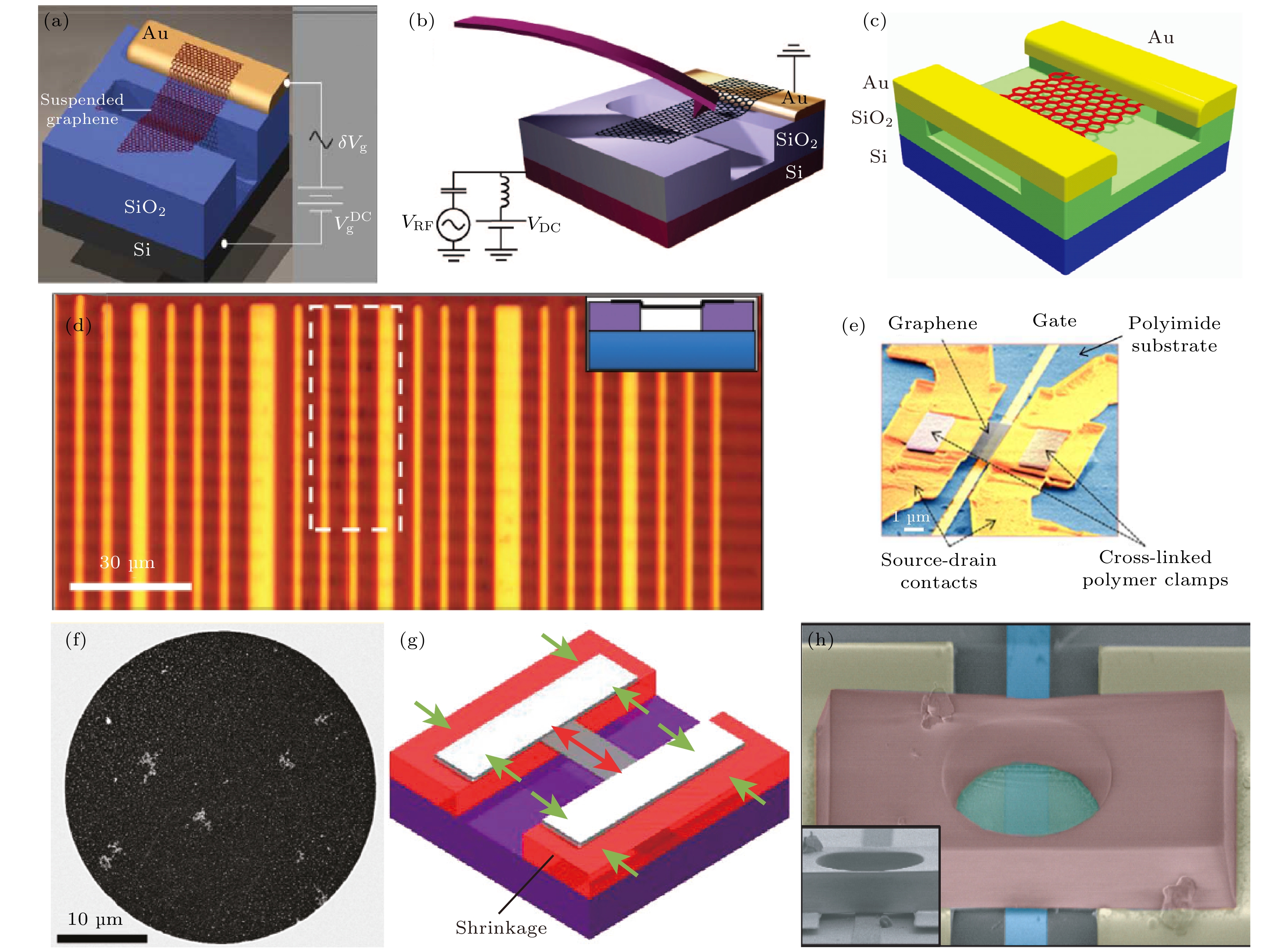
图 1 不同大学制作的石墨烯谐振器结构示意图 (a) 康奈尔大学[53]; (b) 巴塞罗那自治大学[54]; (c) 哥伦比亚大学[57]; (d) 康奈尔大学(阵列式)[58]; (e) 石溪大学[59]; (f) 康奈尔大学(圆形)[60]; (g) 东京大学[61]; (h) 哥伦比亚大学[62]
Fig. 1. Schematic diagrams of the structure of graphene resonators made by different universities: (a) Cornell University[53]; (b) Autonomous University of Barcelona[54]; (c) Columbia University[57]; (d) Cornell University (array) [58]; (e) Shixi University[59]; (f) Cornell University (circular) [60]; (g) University of Tokyo[61]; (h) Columbia University[62].
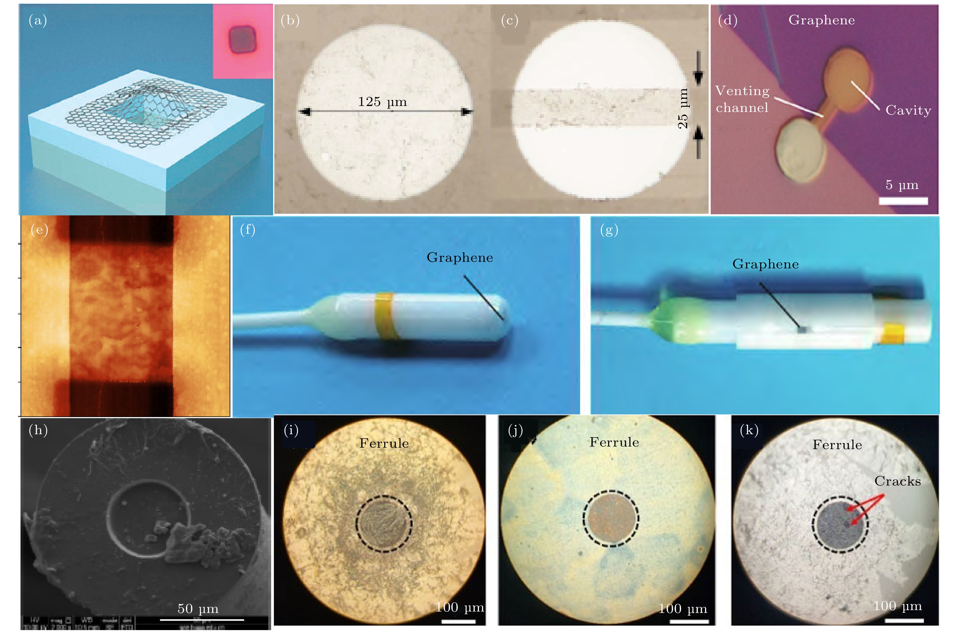
图 2 石墨烯谐振式压力传感器结构示意图 (a) 康奈尔大学制作的石墨烯谐振器的光学图像[65]; (b) 香港理工大学使用的陶瓷插芯[66]; (c) 香港理工大学使用的石墨烯纳米带[66]; (d) 代尔夫特大学制造的哑铃形挤压膜石墨烯压力传感器[67]; (e) 原子力显微镜下的悬浮石墨烯束, 其中氧化物为黑色, 石墨烯束为橙色[68]; (f) 封闭腔式 F-P 谐振传感器[69]; (g) 开放腔式 F-P 谐振传感器[69]; (h) 单模光纤与石英毛细管熔接制成的石墨烯谐振探头[70]; (i) 经丙酮蚀刻处理后的插芯上石墨烯膜显微图像[71]; (j) 350 ℃退火处理的插芯上石墨烯膜显微图像[71]; (k) 经丙酮蚀刻和退火处理的插芯上石墨烯膜显微图像[71]
Fig. 2. Schematic diagram of the structure of graphene resonant pressure sensor: (a) Optical image of graphene resonator made by Cornell University[65]; (b) ceramic ferrules used by the Hong Kong Polytechnic University[66]; (c) graphene nanoribbons used by the Hong Kong Polytechnic University[66]; (d) dumbbell shaped squeeze-film graphene pressure sensor made by Delft University[67]; (e) suspended graphene beam under atomic force microscope, in which the oxide is black and the graphene beam is orange[68]; (f) closed cavity F-P resonant sensor[69]; (g) open cavity F-P resonant sensor[69]; (h) graphene resonant probe made by fusion of single-mode optical fiber and quartz capillary[70]; (i) microscopy image of graphene on the ferrule treated by acetone etching[71]; (j) microscopy image of graphene on the ferrule treated by 350 ℃ annealing[71]; (k) microscopy image of graphene on the ferrule treated by acetone etching and annealing[71].

图 3 石墨烯谐振式加速度计结构及其性能测试 (a) 韩国国立交通大学设计的石墨烯谐振式加速度计[73]; (b) 在石墨烯谐振式加速度计上附着微小质量[74]; (c) 不同附着质量的频率-加速度关系曲线[74]; (d) 美国哥伦比亚大学设计的鼓式石墨烯谐振式加速度计[62]; (e) 中国国防科技大学设计的石墨烯谐振加速度计[76]
Fig. 3. Structure and performance test of graphene resonant accelerometer: (a) Graphene resonant accelerometer designed by Korea National Jiaotong University[73]; (b) small mass attached to graphene resonant accelerometer[74]; (c) accelerations against frequency for different attached masses[74]; (d) drum graphene resonant accelerometer designed by Columbia University, USA[62]; (e) graphene resonant accelerometer designed by National University of Defense Technology, China[76].
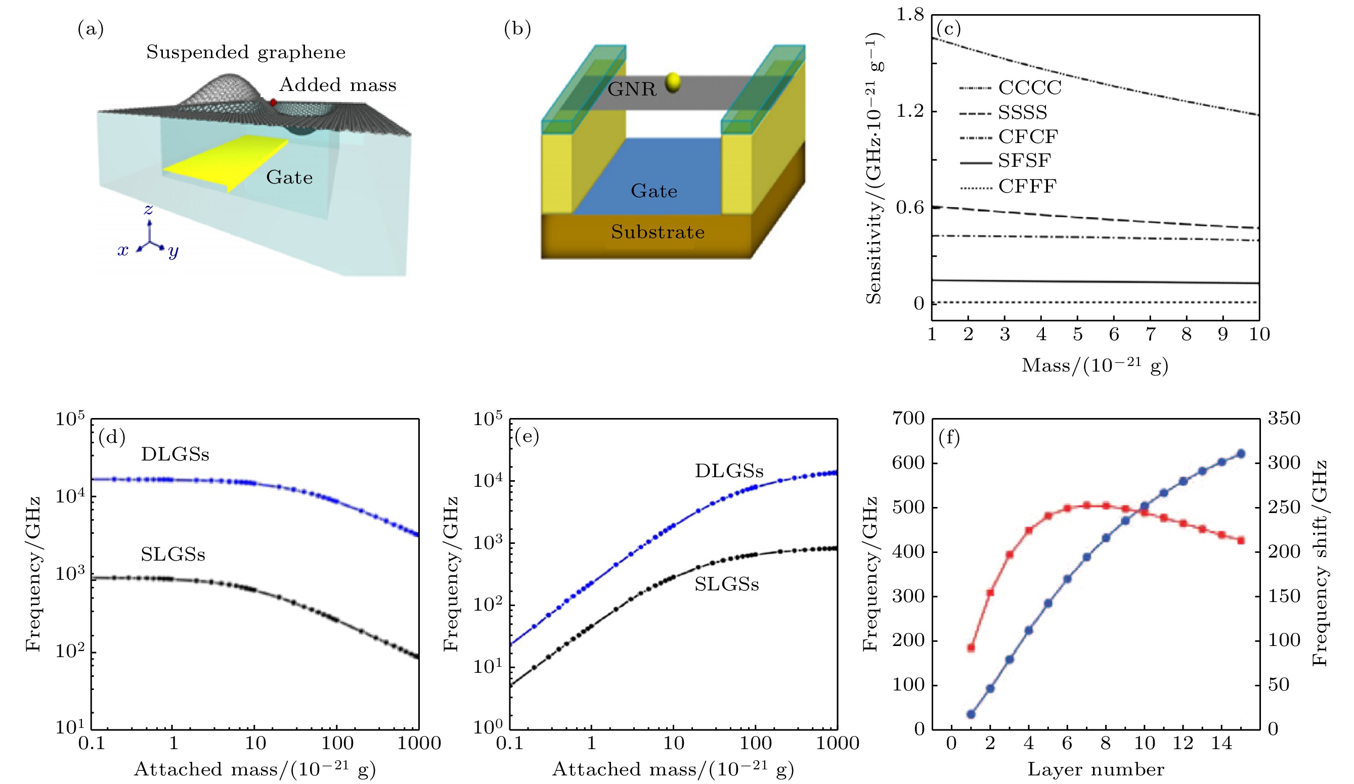
图 4 石墨烯谐振式质量传感器及其性能表征 (a) 查尔姆斯理工大学设计的石墨烯谐振式质量传感器[78]; (b) 韩国世明大学设计的石墨烯谐振式质量传感器[83]; (c) 石墨烯谐振式质量传感器在不同边界条件下的灵敏度[84]; (d) 单层和多层石墨烯的谐振频率-质量变化曲线[85]; (e) 单层和多层石墨烯的谐振频移-质量变化曲线[85]; (f) 谐振频率和频移与质量的关系曲线, 蓝色曲线表示谐振频率随石墨烯层数的变化, 红色曲线表示频移随石墨烯层数的变化[86]
Fig. 4. Graphene resonant mass sensor and its performance characterization: (a) Graphene resonant mass sensor designed by Chalmers University of Technology[78]; (b) graphene resonant mass sensor designed by Semyung University[83]; (c) sensitivity of graphene resonant mass sensor under different boundary conditions[84]; (d) resonant frequency mass variation curve of monolayer/multilayer graphene films[85]; (e) frequency shift mass curve of monolayer/multilayer graphene films[85]; (f) relation curve of resonant frequency and frequency shift with mass, the blue curve represents the change of resonant frequency with the number of graphene layers, and the red curve is the change of frequency shift [86].
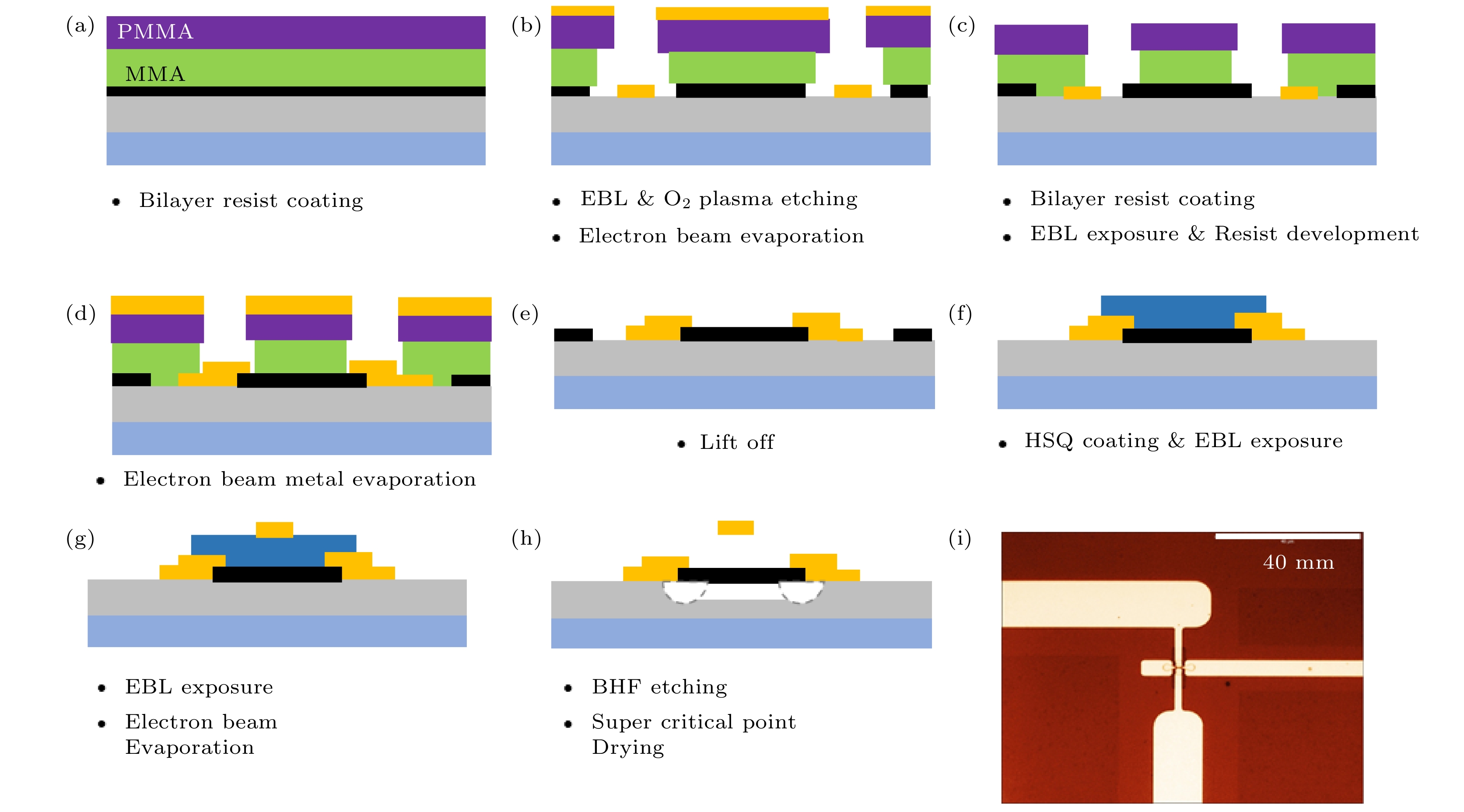
图 5 日本北陆先端科学技术大学制作的石墨烯谐振式质量传感器[88] (a)—(h) 在285 nm厚的SiO2衬底上使用CVD法得到的石墨烯来制作石墨烯谐振器的工艺流程; (i) 制作的石墨烯谐振器光学图像
Fig. 5. Process of graphene resonant mass sensor produced by Japan Advanced Institute of Science and Technology[88]: (a)—(h) Schematic diagrams of top gated graphene resonator fabrication processes with CVD graphene on Si substrate with 285 nm SiO2; (i) optical image of the fabricated top-gated graphene resonator.
表 1 石墨烯谐振器性能指标对比
Table 1. Comparison of performance indicators of graphene resonant pressure sensors.
制备方法 层数 固支方式 谐振频率f/MHz 品质因数Q 激励
方式检测
方式实验环境
(温度, 压强P/Pa)文献 机械剥离法 1—224 双端固支 1—170 20—850 电学/
空间光空间光 室温, P < 1.3×10⁻⁴ [53] 1 双端固支 30—120
30—120125
14000电学 电学 室温, P < 1.3×10⁻³;
5 K, P < 1.3×10⁻³[57] <5 双端固支 108—122 — 电学 电学 室温, P < 6.7 [59] ~31 圆形固支 1—30 2400±300 空间光 空间光 室温, P < 0.79 [60] 2—5 双端固支 8—23 7000 热噪声 电学 室温, P < 10–3 [61] 1 圆形固支 15.7 120 空间光 空间光 室温, P = 1.013×10⁵ [64] 1 周边固支 30—90 25 空间光 空间光 室温, P = 27—3×10⁴ [65] ~30 圆形固支 12—16 1—100 空间光 空间光 室温, P = 8×10²—105 [67] CVD法 1 双端固支 5—75 25
9000电学/
空间光电学/
空间光室温, P < 6.7×10⁻³;
10 K, P < 6.7×10⁻³[58] 30—60 双端固支 0.060—0.204 81—103 光纤光 光纤光 室温, P = 10–2—105 [66] ~13 圆形固支 0.509—0.542 13.3—16.6 光纤光 光纤光 室温, P = 105—2.99×10⁵ [69]  下载: 导出CSV
表 2 石墨烯谐振式压力传感器性能指标对比
Table 2. Comparison of performance indicators of graphene resonant pressure sensors.
层数/层 形状 长度或
直径/μm激励
方式检测
方式测压范围/Pa 谐振频率f 品质因数Q
(室温)压力灵敏度
(kHz·kPa–1)文献 1—75 正方形 4.75 空间光 空间光 10–4—105 30—
90 MHz~25 — [65] 多层 圆形 125 光纤光 光纤光 10–2—105 60—204 kHz 81—103 / [66] 少层 圆形 5 空间光 空间光 8×10²—105 12—
16 MHz1—100 10—90 [67] 多层 正方形 4 空间光 空间光 102—105 15.5—
25.5 MHz50—80 1.65—3.10 [68] 13 圆形 125 光纤光 光纤光 (1—2.99)×105 509—
542 kHz13.3—16.6 0.135 [69] 10 圆形 125 光纤光 光纤光 0—6.895×10⁴ 1.43—
1.64 MHz10.2—13.9 2.93 [70] 10 圆形 125 光纤光 光纤光 2—105 481—
760 kHz110—1034 1—110.4 [71]
下载: 导出CSV
表 3 石墨烯谐振式加速度计性能指标对比
Table 3. Comparison of performance indicators of graphene resonant accelerations.
下载: 导出CSV
表 4 石墨烯谐振式质量传感器仿真性能指标对比
Table 4. Comparison of simulation performance indicators of graphene resonant mass sensors.
下载: 导出CSV
-
[1] Tabata O, Yamamoto T 1999 Sensors and Actuators 75 53
Google Scholar
[2] 樊尚春, 朱黎明, 邢维巍 2019 计测技术 39 4
Google Scholar
Fan S C, Zhu L M, Xing W W 2019 Metrology and Measurement Technology 39 4
Google Scholar
[3] Stachiv I, Gan L 2019 Materials 21 3593
Google Scholar
[4] Su S X P, Yang H S, Agino A M 2005 IEEE Sens. J. 5 1214
Google Scholar
[5] Nie J, Meng X, Li N, Lin L 2017 Sens. Actuat. B Chem. 256 1
Google Scholar
[6] Yu X, Chen X, Ding X, Zhao X 2017 IEEE Trans. Instrum. Meas. 67 1
Google Scholar
[7] Li C, Zhang Q W, Zhao Y L, Tian C, Li B, Han C, Bai B 2021 J. Micromech. Microeng. 31 115001
Google Scholar
[8] John G, Troy W 1993 Sens. Actuat. A Phys. 37 82
Google Scholar
[9] Ikeda K, Kuwayama H, Kobayashi T, Watanabe T, Nishikawa T, Yoshida T, Harada K 1990 Sens. Actuat. A Phys. 21 146
Google Scholar
[10] Chen F, Gao J, Tian W 2017 Sens. Actuat. A Phys. 269 427
Google Scholar
[11] Lei F, Dupuis P, Durrieu O, Zissis G, Maussion P 2017 IEEE Trans. Ind. Electron. 53 5988
Google Scholar
[12] 樊尚春, 孙苗苗, 李成 2012 传感技术学报 25 1
Google Scholar
Fan S C, Sun M M, Li C 2012 J. Trans. Technology 25 1
Google Scholar
[13] Novoselov K S, Geim A K, Morozov S V, Jiang D, Zhang Y, Dubonos S V, Grigorieva I V, Firsov A A 2004 Science 306 5696
Google Scholar
[14] Zhang Y B, Tan Y W, Stormer H L, Kim P 2005 Nature 438 201
Google Scholar
[15] Geim A K, Novoselov K S 2007 Nat. Mater. 6 183
Google Scholar
[16] Geim A K 2009 Science 324 1530
Google Scholar
[17] Rao C N, Sood A K, Subrahmanyam K S, Govindaraj A 2010 Angew. Chem. Int. Ed. Engl. 48 7752
Google Scholar
[18] Smith B R, Conger M J, Mcmullen J S, Neubert M J 2019 J. Bus. Ventur. Insights 11 1
Google Scholar
[19] Cabrera H, Mendoza D, Benítez J L, Bautista F C, Alvarado S, Marín E 2015 J. Phys. D: Appl. Phys. 48 465501
Google Scholar
[20] De S, Coleman J N 2010 Acs Nano. 4 2713
Google Scholar
[21] Nika D L, Askerov A S, Balandin A A 2012 Nano Lett. 12 3238
Google Scholar
[22] Pang C, Lee G Y, Kim T I, Sang M K, Hong N K, Ann S H, Sun K Y 2012 Nat. Mater. 11 795
Google Scholar
[23] Ding G, Li X, Xu Z, Chen H, Wang M 2021 IEEE Electr. Device Lett. 42 236
Google Scholar
[24] Jung M. W, Myung S, Kim K W, Song W, Jo Y Y, Lee S S, Lim J, Park C Y, An K S 2014 Nanotechnology 25 285302
Google Scholar
[25] Jaakkola K, Sandberg H, Lahti M, Ermolov V 2019 IEEE Trans. Compon. Pack. Manuf. Technol. 9 1
Google Scholar
[26] Lee H, Choi T K, Lee Y B, Cho H R, Ghaffari R, Wang L, Kim D H 2016 Nat. Nanotechnol. 11 566
Google Scholar
[27] Seo D H, Pineda S, Fang J, Gozukara Y, Yick S, Bendavid A. Lam S K H, Murdock A T, Murphy A B, Han Z J 2017 Nat. Commun. 8 14217
Google Scholar
[28] 黄乐, 张志勇, 彭练矛 2017 物理学报 66 218501
Google Scholar
Huang L, Zhang Z Y, Peng L M 2017 Acta Phys. Sin. 66 218501
Google Scholar
[29] 赵鹏程, 樊尚春 2017 计测技术 37 4
Google Scholar
Zhao P C, Fan S C 2017 Metro. Measure. Technol. 37 4
Google Scholar
[30] Stankovich S, Dikin D A, Piner R D, Kohlhaas K A, Kleinhammes A, Jia Y, Ruoff R S 2007 Carbon 45 1558
Google Scholar
[31] Ju H M, Huh S H, Choi S H, Lee H L 2010 Mater. Lett. 64 357
Google Scholar
[32] Wang H, Robinson J T, Li X, Dai H 2009 J. Am. Chem. Soc. 131 9910
Google Scholar
[33] Reina A, Jia X, Ho J, Nezich D, Son H, Bulovic V, Kong J 2009 Nano Lett. 9 3087
Google Scholar
[34] Li X, Cai W, An J, Kim S, Nah J, Yang D, Ruoff R S 2009 Science 324 1312
Google Scholar
[35] Sprinkle M, Ruan, Hu Y, Hankinson J, Rubio-Roy M, Zhang B, Wu X, Berger C, de Heer W A 2010 Nat. Nanotechnol. 5 727
Google Scholar
[36] Liang X, Sperling B A, Calizo I, Cheng G, Hacker C A, Zhang Q, Richter C A 2011 ACS Nano. 22 9144
Google Scholar
[37] Li X, Zhu Y, Cai W, Borysiak M, Han B, Chen D, Ruoff R S 2009 Nano Lett. 9 4359
Google Scholar
[38] Lee Y, Bae S, Jang H, Jang S, Zhu S E, Sim S H, Ahn J H 2010 Nano Lett. 10 490
Google Scholar
[39] Chandrashekar B N, Deng B, Smitha A S, Chen Y, Tan C, Zhang H, Liu Z F 2015 Adv. Mater. 27 5210
Google Scholar
[40] Kim K S, Zhao Y, Jang H, Lee S Y, Kim J M, Kim K S, Ahn J H, Kim P, Choi J Y, Hong B H 2009 Nature 457 706
Google Scholar
[41] Lin Y C, Jin C, Lee J C, Jen S F, Suenaga K, Chiu P W 2011 ACS Nano 5 2362
Google Scholar
[42] Lin Y C, Lu C C, Yeh C H, Jin C, Suenaga K, Chiu P W 2011 Nano Lett. 12 414
Google Scholar
[43] Bae S, Kim H, Lee Y, Xu X, Park J S, Zheng Y, Balakrishnan J, Lei T, Kim H R, Song Y I, Kim Y J, Kim K S, Ozyilmaz B, Ahn J H, Iijima S 2010 Nat. Nanotechnology 5 574
Google Scholar
[44] Kitipornchai S, He X Q, Liew K M 2005 Phys. Rev. B 72 075443
Google Scholar
[45] Sakhaee-Pour A, Ahmadian M T, Naghdabadi R 2008 Nanotechnology 19 085702
Google Scholar
[46] Atalaya J, Isacsson A, Kinaret J M 2008 Nano Lett. 8 4196
Google Scholar
[47] Murmu T, Pradhan S C 2009 J. Appl. Phys. 105 064319
Google Scholar
[48] Kwon O K, Lee G Y, Hwang H J, Kang J W 2012 Phys. E Low Dimens. Syst. Nanostruct. 45 194
Google Scholar
[49] Kwon O K, Lee J H, Park J, Kim K S, Kang J W 2013 Curr. Appl. Phys. B 13 360
Google Scholar
[50] Kang J W, Hwang H J, Kim K S 2012 Comput. Mater. Sci. 65 216
Google Scholar
[51] Kang J W, Kim H W, Kim K S, Lee J H 2013 Curr. Appl. Phys. 13 789
Google Scholar
[52] Young K S, Cho S Y, Won K J, Kuen K O 2013 Phys. E Low Dimens. Syst. Nanostruct. 54 118
Google Scholar
[53] Bunch J S, van der Zande A M, Verbridge S S, Frank I W, Tanenbaum D M, Parpia J M, McEuen P L 2007 Science 315 490
Google Scholar
[54] Garcia-Sanchez D, van der Zande A M, Paulo A S, Lassagne B, McEuen P L, Bachtold A 2008 Nano Lett. 8 1399
Google Scholar
[55] Kim S Y, Park H S 2009 Nano Lett. 9 969
Google Scholar
[56] Jiang J W, Wang J S 2012 J. Appl. Phys. 111 054314
Google Scholar
[57] Chen C, Rosenblatt S, Bolotin K I, Kalb W, Kim P, Kymissis I, Hone J 2009 Nat. Nanotechnol. 4 861
Google Scholar
[58] van der Zande A M, Barton R. A, Alden J S, Ruiz-Vargas C S, Whitney W S, Pham P H Q, McEuen P L 2010 Nano Lett. 10 4869
Google Scholar
[59] Guan F, Kumaravadivel P, Averin D V, Du X 2015 Appl. Phys. Lett. 107 193102
Google Scholar
[60] Barton R A, Ilic B, van der Zande A M, Whitney W S, McEuen P L, Parpia J M, Craighead H G 2011 Nano Lett. 11 1232
Google Scholar
[61] Oshidari Y, Hatakeyama T, Kometani R, Warisawa S, Ishihara S 2012 Appl. Phys. Express 5 117201
Google Scholar
[62] Lee S, Chen C, Deshpande V V, Lee G H, Lee I, Lekas M, Hone J 2013 Appl. Phys. Lett. 102 153101
Google Scholar
[63] Al-Mashaal A K, Wood G S, Torin A, Mastropaolo E, Newton M J, Cheung R 2018 IEEE Sens. J. 1 465
Google Scholar
[64] Miller D, Alemán B 2019 Appl. Phys. Lett. 115 193102
Google Scholar
[65] Bunch J S, Verbridge S S, Alden J S, van der Zande A M, Parpia J M, Craighead H G, McEuen P L 2008 Nano Lett. 8 2548
Google Scholar
[66] Ma J, Jin W, Xuan H, Wang C, Ho H L 2014 Opt. Lett. 39 4769
Google Scholar
[67] Dolleman R J, Davidovikj D, Cartamil-Bueno S J, van der Zant H S J, Steeneken P G 2016 Nano Lett. 16 568
Google Scholar
[68] Vollebregt S, Dolleman R J, van der Zant H S J, et al. 2017 19 th International Conference on Solid-State Sensors, Actuators and Microsystems (TRANSDUCERS) Kaohsiung, Taiwan, June 18–20, 2017 pp770–773
[69] Li C, Lan T, Yu X, Bo N, Dong J, Fan S C 2017 Nanomaterials 7 366
Google Scholar
[70] 李子昂, 樊尚春, 李成 2019 计测技术 39 36
Google Scholar
Li Z A, Fan S C, Li C 2019 Metro. Measure. Techno. 39 36
Google Scholar
[71] Liu Y J, Li C, Fan S C, Song X F 2022 Photonic Sens. 12 140
Google Scholar
[72] Lee M, Davidovikj D, Sajadi B, Šiškins M, Alijani F, van der Zant H S J, Steeneken P G 2019 Nano Lett. 19 5313
Google Scholar
[73] Kang J W, Lee J H, Hwang H J, Kim K S 2012 Phys. Lett. A 376 3248
Google Scholar
[74] Byun K R, Kim K S, Hwang H J, Kang J W 2013 J. Comput. Theor. Nanosci. 10 1886
Google Scholar
[75] Kwon O K, Hwang H J, Kang J W 2014 J. Comput. Theor. Nanosci. 82 280
Google Scholar
[76] Jie W, Hu F, Wang X, Qin S 2017 Second International Conference on Photonics and Optical Engineering Xian, China, October 14–17, 2017 p102562 E
[77] Sakhaee-Pour A, Ahmadian M T, Vafai A 2008 Solid State Commun. 145 168
Google Scholar
[78] Atalaya J, Kinaret J M, Isacsson A 2009 EPL 91 48001
Google Scholar
[79] Dai M, Kim C W, Eom K 2012 Nanoscale Res. Lett. 7 499
Google Scholar
[80] Jiang J W, Park H S, Rabczuk T 2012 Nanotechnology 23 475501
Google Scholar
[81] Arash B, Wang Q, Duan W H 2011 Phys. Lett. A 375 2411
Google Scholar
[82] Lei X W, Natsuki T, Shi J X, Ni Q Q 2013 J. Appl. Phys. 113 154313
Google Scholar
[83] Kwon O K, Kim K S, Park J, Kang J W 2012 Comput. Mater. Sci. 67 329
Google Scholar
[84] Lee H L, Hsu J C, Lin S Y, Chang W J 2013 J. Appl. Phys. 114 123506
Google Scholar
[85] Natsuki T, Shi J X, Ni Q Q 2013 J. Appl. Phys. 114 094307
Google Scholar
[86] Gong X, Jiang S, Wang X, Liu S, Wang S 2014 15 th International Conference on Electronic Packaging Technology Chengdu, China, August 12–15, 2014 p511
[87] Desai S H, Pandya A A, Panchal M B 2021 J. Phys. Conf. Ser. 1854 012029
Google Scholar
[88] Muruganathan M, Miyashita H, Kulothungan J, Schmidt M E, Mizuta H 2018 IEEE SENSORS Conference New Delhi, October 28–31, 2018 p1

 下载:
下载:
计量
- 文章访问数: 13673
- PDF下载量: 273
- 被引次数: 0
