


-
利用计算机辅助设计(technology computer aided design, TCAD)软件针对N型阱电阻的单粒子效应开展仿真研究, 结果表明单个重离子入射到N阱电阻中会造成器件输出电流的扰动. 经过对电阻的工作机理和单粒子效应引入的物理机制进行分析, 结果表明重离子在N阱电阻中产生的电子-空穴对中和了N阱电阻中的空间电荷区, 使得N阱电阻的阻抗瞬间减小、电流增大, 且空间电荷区被破坏的面积越大瞬态电流的峰值越高. 随着阱结构中的高浓度过剩载流子被收集, 单粒子效应的扰动会消失. 但N阱电阻独特的长宽比设计导致器件中的过剩载流子收集效率低、单粒子效应对阱电阻的扰动时间长. 文中还对影响N阱电阻单粒子效应的其他因素开展了研究, 结果表明重离子的线性能量传输(linear energy transfer, LET)值越高、入射位置距离输入电极越远, N阱电阻的单粒子效应越严重. 此外, 适当缩短N阱电阻的长度、提高阱电阻的输入电压、降低电路电流可以增强其抗单粒子效应表现.In this paper, the single event effect of N-well resistor is simulated by using the technology computer aided design (TCAD) software. The results indicate that a single heavy ion incident into the N-well resistor will make a disturbance in the output current of the device. The working mechanism of the N-well resistor and the physical mechanism introduced by the single event effect are studied. The results show that ion-induced electron-hole pairs neutralize the depletion region in the N-well substance that provides high impedance for the device, resulting in the instantaneous increase of the output current. The larger the destroyed area of the depletion region in the N-well resistor, the higher the peak value of the transient output current is. But the ion-induced disturbance can disappear with the collection of the high concentration of excess carriers in the N-well structure. However, the unique aspect ratio design of the N-well resistor makes only the carriers close to the input drift to output under the electric field. And, the drift motion of carriers takes a lot of time because of the long transport distance, which leads to low efficiency of collecting excess carriers and a long duration of ion-induced disturbance in the N-well resistor. Besides, some other factors that can affect the single event effect in the N-well resistors are also studied in this paper. The results show that the higher the LET value of ions and the farther the incident location from the input, the more serious the single event effect of N-well resistance is. In addition, properly shortening the length of the N-well resistor and increasing the input voltage of the N-well resistor can enhance its resistance to single event effect.
-
Keywords:
- N-well resistor /
- space charge /
- single event effect /
- transient currrent
[1] 姜秀杰, 孙辉先, 王志华, 张利 2005 电子器件 28 1
 Google Scholar
Jiang X J, Sun H X, Wang Z H, Zhang L 2005 Chin. J. Electron Devices 28 1
Google Scholar
[2] 姜秀杰, 孙辉先 2004 中国空间科学学会空间探测专业委员会学术会议 (中国空间科学学会) 第402—406页
Jiang X J, Sun X H 2004 Academic Conference of Space Exploration Committee of Chinese Society of Space Sciences (China Society of Space Science) pp402–406 (in Chinese)
[3] 卓青青, 刘红侠, 郝跃 2012 物理学报 61 218501
Google Scholar
Zhuo Q Q, Liu H X, Hao Y 2012 Acta Phys. Sin. 61 218501
Google Scholar
[4] 伊腾岳 2019 博士学位论文 (西安: 西安电子科技大学)
Yi T Y 2019 Ph. D. Dissertation (Xi’an: Xidian University) (in Chinese)
[5] 卢超, 陈伟, 罗尹虹, 丁李利, 王勋, 赵雯, 郭晓强, 李赛 2020 物理学报 69 086160
Google Scholar
Lu C, Chen W, Luo Y H, Ding L L, Wang X, Zhao W, Guo X Q, Li S 2020 Acta Phys. Sin. 69 086160
Google Scholar
[6] 毕津顺, 刘刚, 罗家俊, 韩郑生 2013 物理学报 62 208501
Google Scholar
Bi J S, Liu G, Luo J J, Han Z S 2013 Acta Phys. Sin. 62 208501
Google Scholar
[7] Ju A A, Guo H X, Zhang F Q, Ding L L, Du G H, Guo J L, Zhong X L, Wei J N, Pan X Y, Zhang H, 2022 IEEE T. Nucl. Sci. 69 890
Google Scholar
[8] Holberg A 2002 CMOS Analog Circuit Design (Vol. 2) (New York: Oxford Uiversity Press) p43
[9] Guido N 1997 Electrical Overstress/Electrostatic Discharge Symposium 97 221
[10] Atsumi S, Taura T 1998 US Patent 5 986 940 [1998-2-26]
[11] Booth R V H, McAndrew C C 1997 IEEE T. Electron Dev. 44 809
[12] Singh R K, Roy J N 2006 Solid-State Electron. 50 1696
Google Scholar
[13] 李月影, 李冰, 何小东 2007 电子与封装 7 39
Google Scholar
Li Y Y, Li B, He X D 2007 Electron. Packag. 7 39
Google Scholar
[14] 石晓峰, 罗宏伟, 李斌 2009 电子元件与材料 28 9
Google Scholar
SHI X F, Luo H W, Li B 2009 Electron. Compon. mater. 28 9
Google Scholar
[15] Srinivasan P, Xiong W, Zhao S 2010 IEEE Electron Dev. Lett. 31 1476
Google Scholar
[16] Luo J, Wang T S, Li D Q, Liu T Q, Hou M D, Sun Y M, Duan J L, Yao H J, Xi K, Ye B, Liu J 2018 Chin. Phys. B 27 076101
Google Scholar
[17] 韩兆芳, 虞勇坚 2014 电子与封装 16 45
Google Scholar
Han Z F, Yu Y J 2014 Electron. Packag. 16 45
Google Scholar
[18] 王天岐, 2016 博士毕业论文 (哈尔滨: 哈尔滨工业大学)
Wang T Q 2016 Ph. D. Dissertation (Harbin: Harbin Institute of Technology University) (in Chinese)
[19] 张晋新, 郭红霞, 郭旗, 文林, 崔江维, 席善斌, 王信, 邓伟 2013 物理学报 62 048501
Google Scholar
Zhang J X, Guo H X, Guo Q, Wen L, Cui J W, Xi S B, Wang X, Deng W 2013 Acta Phys. Sin. 62 048501
Google Scholar
[20] 程佳 2016 硕士毕业论文 (北京: 中国科学院大学)
Chen J 2016 M. S. Dissertation (Beijing: University of Chinese Academy of Sciences) (in Chinese)
[21] Koike H, Otsuki T, Kimura T, Fukuma M, Hayashi Y, Maejima Y, Amanuma K, Tanabe N, Matsuki T, Saito S, Takeuchi T, Kobayashi S, Kunio T, Hase T, Miyasaka Y, Shohata N, Takada M 1996 IEEE J. Solid-St. Circ. 31 1625
Google Scholar
[22] 刘蓉容 2016 硕士毕业论文 (长沙: 国防科学技术大学)
Liu Y Y 2016 M. S. Dissertation (Changsha: National University of Defense Technology) (in Chinese)
[23] Wang Q Q, Liu H X, Wang S L, Chen S P 2018 IEEE T. Nucl. Sci. 65 2250
Google Scholar
-
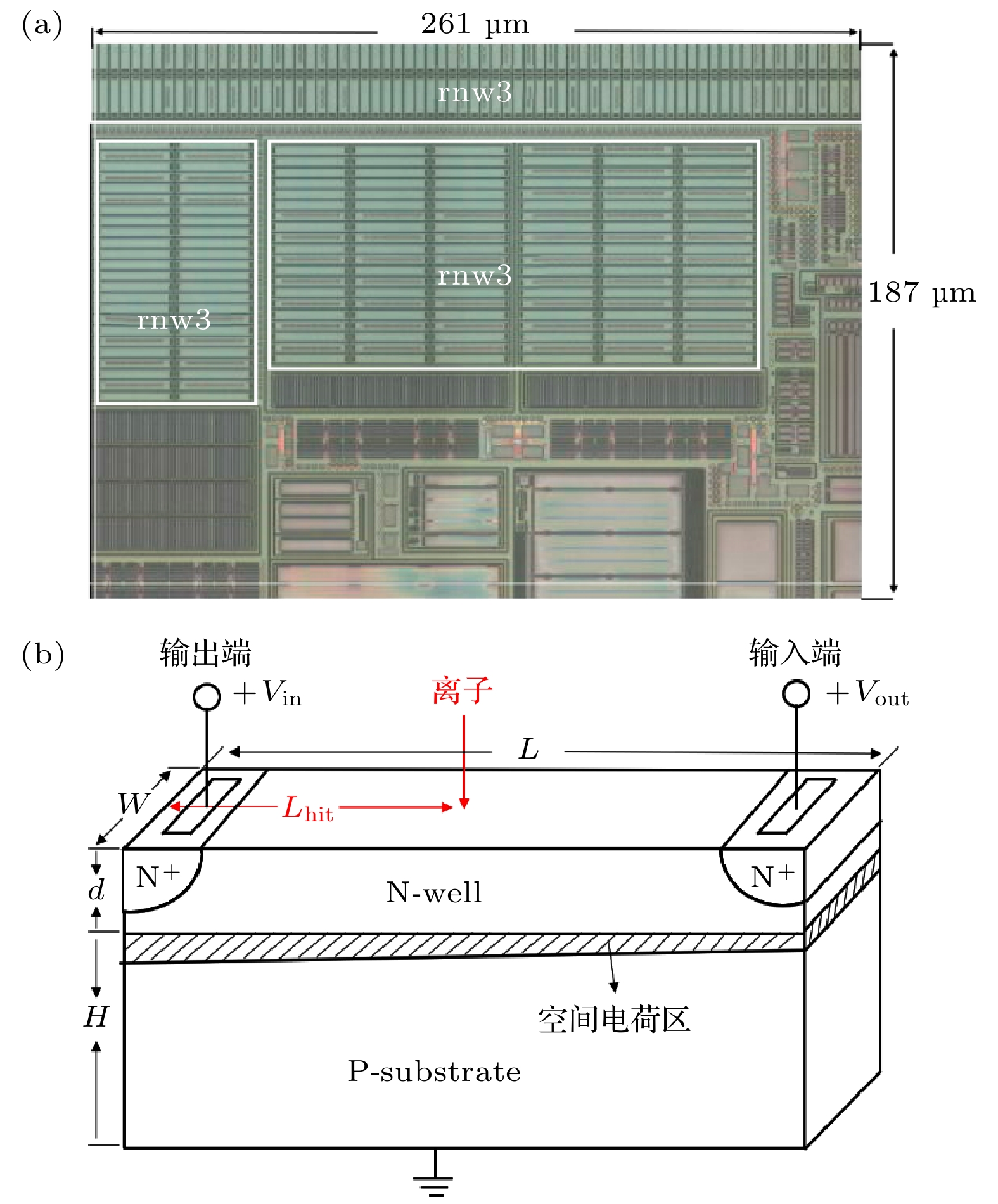
图 1 N阱结构示意图 (a)位于一款存储器外围电路中的N阱电阻, 图中的rnw3表示三端N阱电阻; (b) N阱电阻的三维结构示意图
Fig. 1. Structure diagram of the N-well resistor: (a) An N-well resistor located in a memory peripheral circuit, rnw3 in the figure represents a three terminal N-well resistor; (b) the three-dimensional structure of N well resistor.
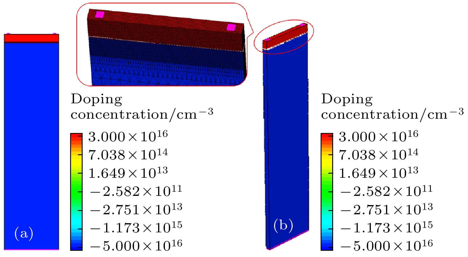
图 2 N阱电阻TCAD模型示意图 (a)二维模型; (b)三维模型
Fig. 2. The diagram of N well resistor TCAD model: (a) Two-dimension model; (b) three-dimension model.
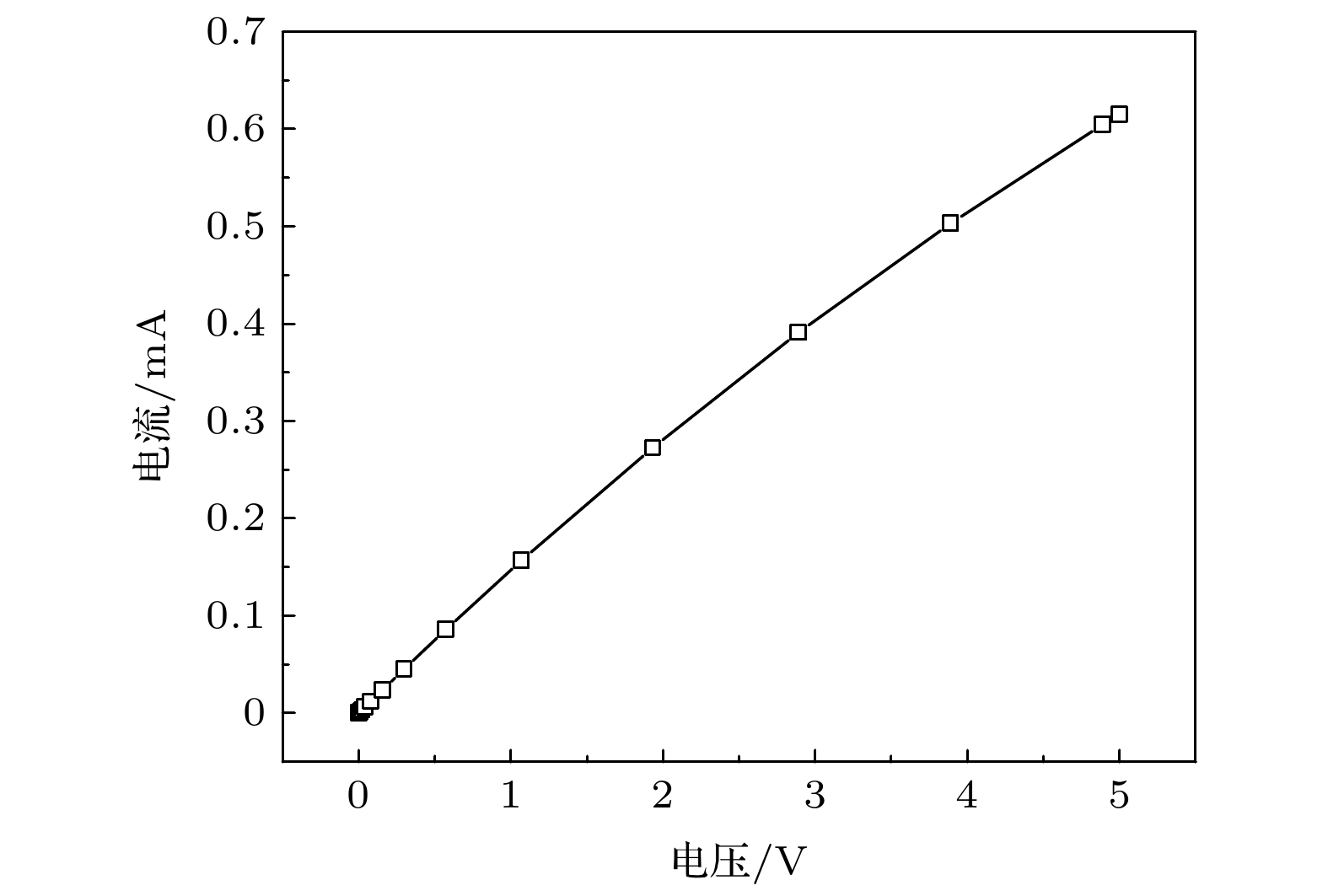
图 3 N阱电阻输出电流随输入电压的变化情况
Fig. 3. The output current versus the input voltage of the N-well resistor.

图 4 在不同输出电压下, 重离子在三维N阱电阻模型中产生的瞬态电流
Fig. 4. Ion-induced transient current in the three-dimensional model of N-well resistor under different output voltage.
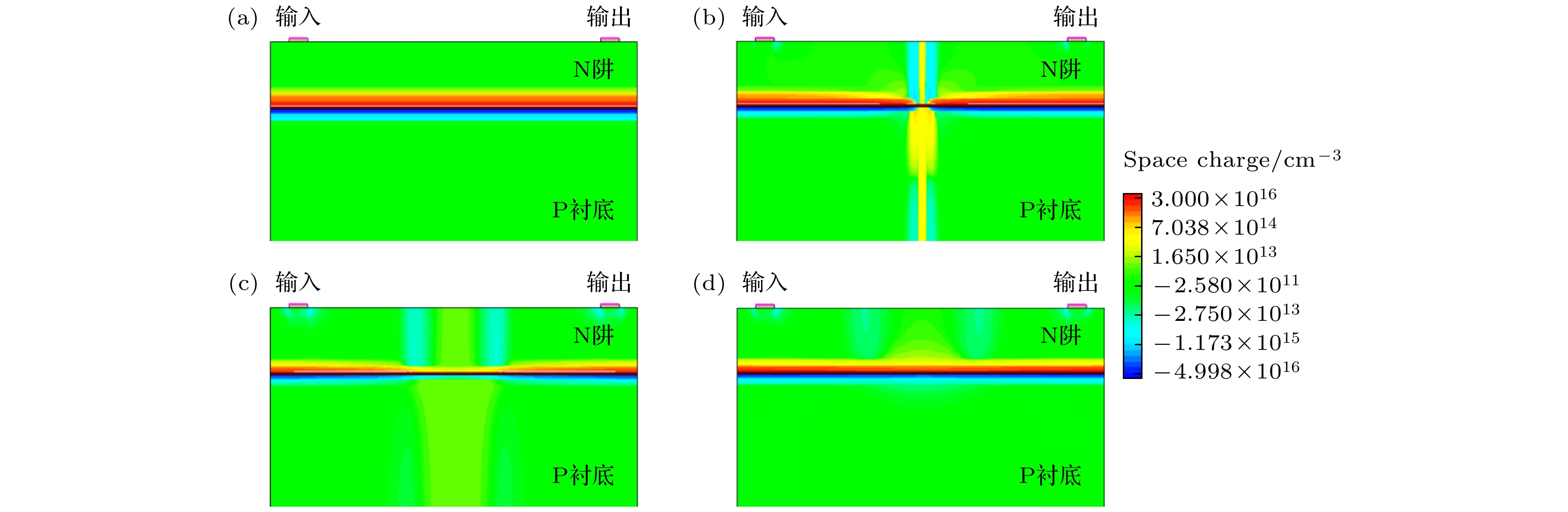
图 5 输出电压为3.3 V时, 不同时刻内N阱电阻内空间电荷区分布 (a) 0 ns; (b) 0.1 ns; (c) 0.6 ns; (d) 5 ns
Fig. 5. When output voltage of model is 3.3 V, the space charge distribution in N well resistor at : (a) 0 ns; (b) 0.1 ns; (c) 0.6 ns; (d) 5 ns.

图 6 两种不同电压条件下, N阱结构中深度为2 μm处的位置上横向电场强度在不同时刻的分布情况 (a) 输出端电压为3.3 V; (b) 输出端电压为0 V
Fig. 6. The distribution of transverse electric field in N well structure at depth of 2 μm location: (a) Output voltage is 3.3 V; (b) output voltage is 0 V.
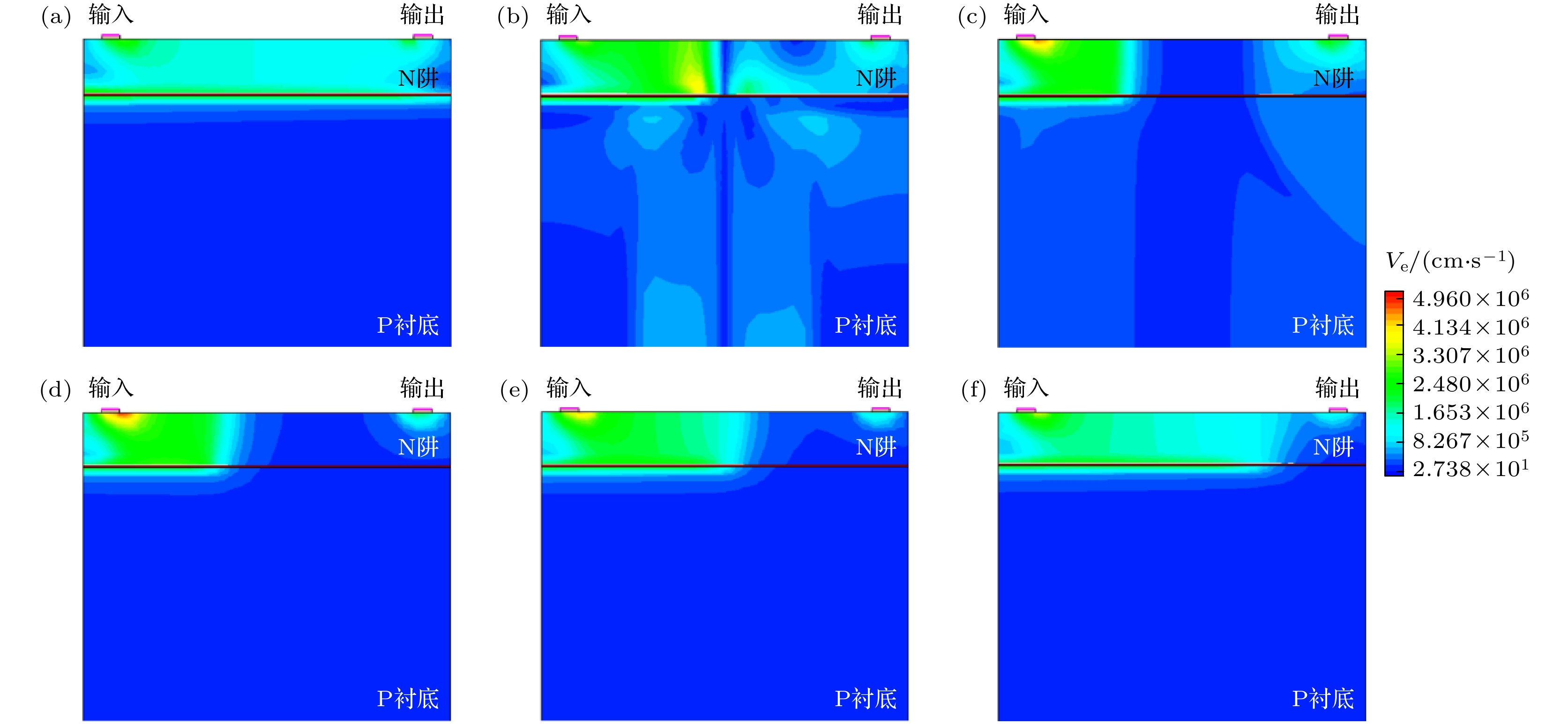
图 7 输出电压为0 V时, 不同时刻内N阱中电子速度分布 (a) 0 ns; (b) 0.1 ns; (c) 0.6 ns; (d) 5 ns; (e) 15 ns ; (f) 30 ns
Fig. 7. When output voltage is 0 V, the distribution of electron velocity in N well structure at: (a) 0 ns, (b) 0.1 ns, (c) 0.6 ns, (d) 5 ns, (e) 15 ns and (f) 30 ns moment.

图 8 输出电压为0 V时, 不同时刻内N阱电阻中空间电荷区的变化 (a) 0 ns; (b) 0.1 ns; (c) 0.6 ns; (d) 5 ns; (e) 15 ns ; (f) 30 ns
Fig. 8. When output voltage is 0 V, the change of space charge region in N well structure at (a) 0 ns, (b) 0.1 ns, (c) 0.6 ns, (d) 5 ns, (e) 15 ns, (f) 30 ns moment.

图 9 重离子从不同位置入射N阱电阻产生的单粒子瞬态电流
Fig. 9. Single event transient current in N-well resistor generated by ion from different incident locations.

图 10 不同LET值的重离子在N阱电阻中产生的瞬态电流
Fig. 10. Single event transient current in N-well resistor generated by ions with different LET values.
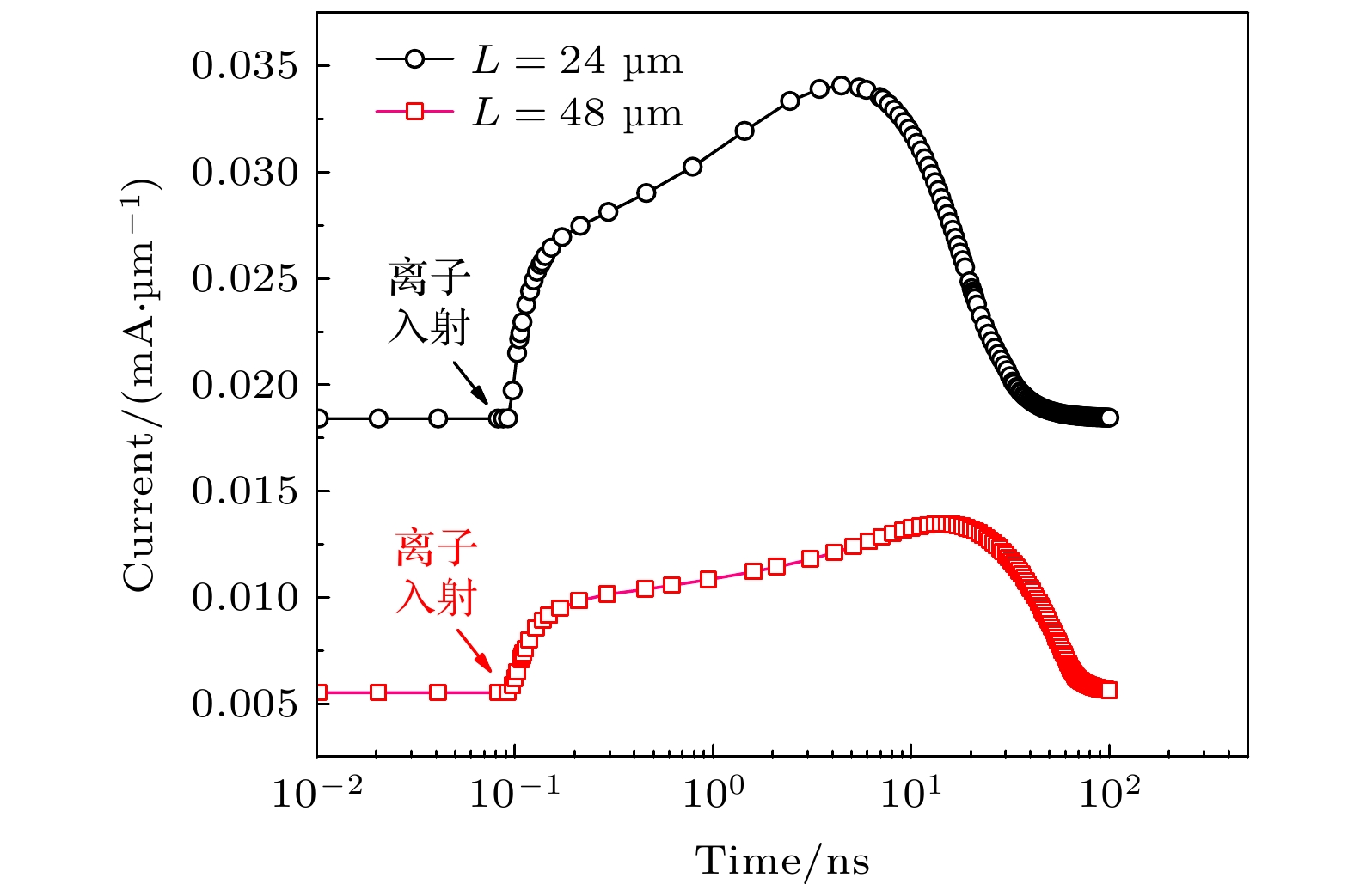
图 11 不同长度的N电阻中产生的归一化单粒子瞬态电流
Fig. 11. Normalization single event transient current generated in N-well resistors with different lengths.
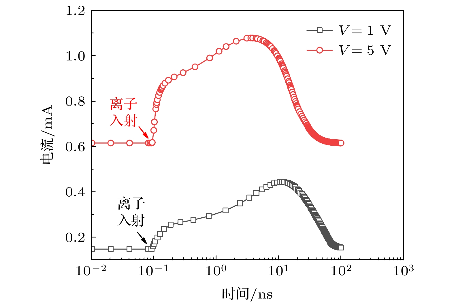
图 12 不同输入电压下的N阱电阻产生的单粒子瞬态电流
Fig. 12. Single event transient current generated in N-well resistors under different input voltage.
表 1 本文模型电阻值与文献[11]中模型电阻值的比较
Table 1. The comparison of calculated resistance values in this paper and results in Ref. [11].
W/μm 本文模型/
kΩ文献中的简单
模型/kΩ文献中的高级
模型/kΩ2.5 17.14 18.21 17.06 5.0 8.10 8.21 7.91 7.0 5.70 5.70 5.53 10.0 4.29 3.91 3.81 注: 输入电压为3 V, N阱和P衬底的掺杂浓度为5×1016 cm3, 长度为100 μm.  下载: 导出CSV
表 2 TCAD模型中所使用的具体参数
Table 2. Detailed parameters used in TCAD models
参数 数值 电阻的长度L/μm 24 电阻的宽度W/μm 2 N阱的深度d/μm 4 N阱的掺杂浓度/(1015 cm–3) 3 P衬底的掺杂浓度/(1015 cm–3) 5 P衬底的深度H/μm 100
下载: 导出CSV
表 3 不同输出端电压下, 重离子在N阱电阻三维模型中产生的瞬态电流参数
Table 3. Detailed parameters of ion-induced transient current in three-dimension model under different output voltage.
输出端
电压/V电流峰
值/mA到达电流峰
值时间/ns瞬态电流
持续时间/ns积分电
荷/pC0 0.81 4.44 63.20 51.56 1.3 0.60 5.44 37.80 33.70 2.3 0.43 5.44 29.40 19.28 3.3 0.25 4.45 17.90 3.03
下载: 导出CSV
-
[1] 姜秀杰, 孙辉先, 王志华, 张利 2005 电子器件 28 1
Google Scholar
Jiang X J, Sun H X, Wang Z H, Zhang L 2005 Chin. J. Electron Devices 28 1
Google Scholar
[2] 姜秀杰, 孙辉先 2004 中国空间科学学会空间探测专业委员会学术会议 (中国空间科学学会) 第402—406页
Jiang X J, Sun X H 2004 Academic Conference of Space Exploration Committee of Chinese Society of Space Sciences (China Society of Space Science) pp402–406 (in Chinese)
[3] 卓青青, 刘红侠, 郝跃 2012 物理学报 61 218501
Google Scholar
Zhuo Q Q, Liu H X, Hao Y 2012 Acta Phys. Sin. 61 218501
Google Scholar
[4] 伊腾岳 2019 博士学位论文 (西安: 西安电子科技大学)
Yi T Y 2019 Ph. D. Dissertation (Xi’an: Xidian University) (in Chinese)
[5] 卢超, 陈伟, 罗尹虹, 丁李利, 王勋, 赵雯, 郭晓强, 李赛 2020 物理学报 69 086160
Google Scholar
Lu C, Chen W, Luo Y H, Ding L L, Wang X, Zhao W, Guo X Q, Li S 2020 Acta Phys. Sin. 69 086160
Google Scholar
[6] 毕津顺, 刘刚, 罗家俊, 韩郑生 2013 物理学报 62 208501
Google Scholar
Bi J S, Liu G, Luo J J, Han Z S 2013 Acta Phys. Sin. 62 208501
Google Scholar
[7] Ju A A, Guo H X, Zhang F Q, Ding L L, Du G H, Guo J L, Zhong X L, Wei J N, Pan X Y, Zhang H, 2022 IEEE T. Nucl. Sci. 69 890
Google Scholar
[8] Holberg A 2002 CMOS Analog Circuit Design (Vol. 2) (New York: Oxford Uiversity Press) p43
[9] Guido N 1997 Electrical Overstress/Electrostatic Discharge Symposium 97 221
[10] Atsumi S, Taura T 1998 US Patent 5 986 940 [1998-2-26]
[11] Booth R V H, McAndrew C C 1997 IEEE T. Electron Dev. 44 809
[12] Singh R K, Roy J N 2006 Solid-State Electron. 50 1696
Google Scholar
[13] 李月影, 李冰, 何小东 2007 电子与封装 7 39
Google Scholar
Li Y Y, Li B, He X D 2007 Electron. Packag. 7 39
Google Scholar
[14] 石晓峰, 罗宏伟, 李斌 2009 电子元件与材料 28 9
Google Scholar
SHI X F, Luo H W, Li B 2009 Electron. Compon. mater. 28 9
Google Scholar
[15] Srinivasan P, Xiong W, Zhao S 2010 IEEE Electron Dev. Lett. 31 1476
Google Scholar
[16] Luo J, Wang T S, Li D Q, Liu T Q, Hou M D, Sun Y M, Duan J L, Yao H J, Xi K, Ye B, Liu J 2018 Chin. Phys. B 27 076101
Google Scholar
[17] 韩兆芳, 虞勇坚 2014 电子与封装 16 45
Google Scholar
Han Z F, Yu Y J 2014 Electron. Packag. 16 45
Google Scholar
[18] 王天岐, 2016 博士毕业论文 (哈尔滨: 哈尔滨工业大学)
Wang T Q 2016 Ph. D. Dissertation (Harbin: Harbin Institute of Technology University) (in Chinese)
[19] 张晋新, 郭红霞, 郭旗, 文林, 崔江维, 席善斌, 王信, 邓伟 2013 物理学报 62 048501
Google Scholar
Zhang J X, Guo H X, Guo Q, Wen L, Cui J W, Xi S B, Wang X, Deng W 2013 Acta Phys. Sin. 62 048501
Google Scholar
[20] 程佳 2016 硕士毕业论文 (北京: 中国科学院大学)
Chen J 2016 M. S. Dissertation (Beijing: University of Chinese Academy of Sciences) (in Chinese)
[21] Koike H, Otsuki T, Kimura T, Fukuma M, Hayashi Y, Maejima Y, Amanuma K, Tanabe N, Matsuki T, Saito S, Takeuchi T, Kobayashi S, Kunio T, Hase T, Miyasaka Y, Shohata N, Takada M 1996 IEEE J. Solid-St. Circ. 31 1625
Google Scholar
[22] 刘蓉容 2016 硕士毕业论文 (长沙: 国防科学技术大学)
Liu Y Y 2016 M. S. Dissertation (Changsha: National University of Defense Technology) (in Chinese)
[23] Wang Q Q, Liu H X, Wang S L, Chen S P 2018 IEEE T. Nucl. Sci. 65 2250
Google Scholar

 下载:
下载:
计量
- 文章访问数: 7899
- PDF下载量: 110
- 被引次数: 0
