


-
氮化镓(GaN)器件的自热问题是目前限制其性能的关键因素, 在GaN材料上直接生长多晶金刚石改善器件的自热问题成为研究的热点, 多晶金刚石距离GaN器件工作有源区近, 散热效率高, 但多晶金刚石和GaN材料热失配可能会导致GaN电特性衰退. 本文采用微波等离子体化学气相沉积法, 在2 in (1 in = 2.54 cm)Si基GaN材料上生长多晶金刚石. 测试结果显示, 多晶金刚石整体均匀一致, 生长金刚石厚度为9—81 μm, 随着多晶金刚石厚度的增大, GaN (002)衍射峰半高宽增量和电性能衰退逐渐增大. 通过激光切割和酸法腐蚀, 将Si基GaN材料从多晶金刚石上完整地剥离下来. 测试结果表明: 金刚石高温生长过程中, 氢原子对氮化硅外延层缺陷位置有刻蚀作用形成孔洞区域, 刻蚀深度可达本征GaN层; 在降温过程, 孔洞周围形成裂纹区域. 剥离下来的Si基GaN材料拉曼特征峰峰位, XRD的(002)衍射峰半高宽以及电性能均恢复到本征状态, 说明多晶金刚石与Si基GaN热失配产生应力, 引起GaN晶格畸变, 导致GaN材料电特性衰退, 这种变化具有可恢复性, 而非破坏性.
-
关键词:
- 多晶金刚石 /
- 氮化镓 /
- 微波等离子体化学气相沉积法 /
- 电性能
Self-heating has become a limited factor for the performance improvement of GaN electronics. Growing polycrystalline diamond directly on GaN material to solve the heating problem of GaN devices has become one of the research highlights. Polycrystalline diamond on Si-based GaN material has the advantages of being close to the channel region and high heat dissipation efficiency. However, there is a problem that the thermal expansion mismatch between polycrystalline diamond and GaN material leads to the deterioration of electrical characteristics of GaN. In this work, we adopt microwave plasma chemical vapor deposition (MPCVD) method to grow polycrystalline diamond on 2-inch Si-based GaN material. The test results show that the polycrystalline diamond is uniform as a whole. The average thickness is in the range of 9–81 μm. With the thickness of polycrystalline diamond increasing, the XRD (002) diffraction peak FWHM increment and mobility loss gradually increase for the Si-based GaN material. Through laser cutting and acid etching, the Si-based GaN material is successfully stripped from the polycrystalline diamond. It is found that during the process of diamond growth at high temperature, hydrogen atoms etch the defect positions of the silicon nitride epitaxial layer, forming a hole area in the GaN, and the etching depth can reach the intrinsic GaN layer. During the process of cooling, a crack area is formed around the hole area. Raman characteristic peaks, full widths at half maximum of XRD (002) diffraction peaks, and electrical properties of the stripped Si-based GaN materials are all returned to their intrinsic states. The above results show that the thermal expansion mismatch between polycrystalline diamond and Si-based GaN introduces stress into GaN, which leads to lattice distortion of GaN lattice and the degradation of electrical property of GaN material. The degradation of GaN material is recoverable, but not destructive.-
Keywords:
- polycrystalline diamond /
- GaN /
- microwave plasma chemical vapor deposition /
- electrical properties
[1] EI Fatimy A, Dyakonova N, Meziani Y, Otsuji T, Knap W, Vandenbrouk S, Madjour K, Théron D, Gaquiere C, Poisson M A, Delage S, Prystawko P, Skierbiszewski C 2010 J. Appl. Phys. 107 024504
 Google Scholar
[2] Marti D, Tirelli S, Alt A R, Roberts J, Bolognesi C R 2012 IEEE Electron Dev. Lett. 33 1372
Google Scholar
[3] Nazari M, Hancock B L, Piner E L, Holtz M W 2015 IEEE Compd. Semicond. Integr. Circuit Symp. 62 1467
Google Scholar
[4] Coe S E, Sussmann R S 2000 Diamond Relat. Mater. 9 1726
Google Scholar
[5] Alomari M, Dipalo M, Rossi S, Diforte-Poisson M A, Delage S, Carlin J F, Grandjean N, Gaquiere C, Toth L, Pecz B, Kohn E 2011 Diamond Relat. Mater. 20 604
Google Scholar
[6] Altman D, Tyhach M, McClymonds J, Kim S, Graham S 2014 Fourteenth Intersociety Conference on Thermal and Thermomechanical Phenomena in Electronic Systems (ITherm) Orlando, USA, May 27–30, 2014 p1199
[7] Anderson T J, Hobart K D, Tadjer M J, Koehler A D, Imhoff E A, Hite J K, Feygelson T I, Pate B B, Eddy Jr C R, Kub F J 2017 ECS J. Solid State Sci. Technol. 6 Q3036
Google Scholar
[8] Hancock B L, Nazari M, Anderson J, Piner E, Faili F, Oh S, Twitchen D, Graham S, Holtz M 2016 Appl. Phys. Lett. 108 211901
Google Scholar
[9] Zhou Y, Ramaneti R, Anaya J, Korneychuk S, Derluyn J, Sun H, Pomeroy J, Verbeeck J, Haenen K, Kubal M 2017 Appl. Phys. Lett. 111 041901
Google Scholar
[10] Ahmed R, Siddique A, Anderson J, Engdahl C, Holtz M, Piner E 2019 Cryst. Growth Des. 19 672
Google Scholar
[11] Siddique A, Ahmed R, Anderson J, Nazari M, Yates L, Graham S, Holtz M, Piner E L 2019 ACS Appl. Electron. Mater. 1 1387
Google Scholar
[12] Malakoutian M, Ren C H, Woo K, Li H, Chowdhury S 2021 Cryst. Growth Des. 21 2624
Google Scholar
[13] 杨士奇, 任泽阳, 张金风, 何琦, 苏凯, 张进成, 郭怀新, 郝跃 2021 固体电子学研究与进展 41 18
Google Scholar
Yang S Q, Ren Z Y, Zhang J F, He Q, Su K, Zhang J C, Guo H X, Hao Y 2021 Res. Prog. SSE 41 18
Google Scholar
[14] Wang A, Tadjer M J, Anderson T J, Baranyai R, Pomer J W 2013 IEEE Trans. Electron Dev. 60 3149
Google Scholar
[15] Tadjer M J, Anderson T J, Hobart K D, Mastro M A, Hite J K, Caldwell J D, Picard Y N, Kub F J, Eddy Jr C R 2010 Electron. Mater. 39 2452
Google Scholar
[16] Sun H, Simon R B P, Pomeroy J W, Francis D, Faili F, Twitchen D J, Kuball M 2015 Appl. Phys. Lett. 106 111906
Google Scholar
[17] Teng Y, Liu D Y, Tang K, Zhao W K, Chen Z A, Huang Y M, Duan J J, Bian Y, Ye J D, Zhu S M, Zhang R, Zheng Y D, Gu S M 2022 Chin. Phys. B 31 128106
Google Scholar
[18] 李俊鹏, 任泽阳, 张金风, 王晗雪, 马源辰, 费一帆, 黄思源, 丁森川, 张进成, 郝跃 2023 物理学报 72 038102
Google Scholar
Li J P, Ren Z Y, Zhang J F, Wang H X, Ma Y C, Fei Y F, Huang S Y, Ding S C, Zhang J C, Hao Y 2023 Acta Phys. Sin. 72 038102
Google Scholar
[19] Sein H, Ahmed W, Jackson M, Ali N, Gracio J 2003 Surf. Coat. Tech. 163 196
Google Scholar
[20] Xie W L, Lv X Y, Wang Q L, Li L A, Zou G T 2022 Chin. Phys. B 31 108106
Google Scholar
[21] Letts E, Key D, Hashimoto T 2016 J. Cryst. Growth 456 27
Google Scholar
[22] Davis R F, Gehrke T, Linthicum K J, Preble E, Rajagopal P, Ronning C, Zorman C, Mehregany M 2001 J. Cryst. Growth 231 335
Google Scholar
[23] Dadgar A, Schulze F, Wienecke M, Gadanecz A, Bläsing J, Veit P, Hempel T, Diez A, Christen J, Krost A 2007 New J. Phys. 9 389
Google Scholar
[24] Kumar M S, Kumar J 2003 Mater. Chem. Phys. 77 341
Google Scholar
[25] Sochacki T, Bryan Z, Amilusik M, Collazo R, Lucznik B, Weyher J L, Nowak G, Sadovyi B, Kamler G, Kucharski R 2013 Appl. Phys. Express 6 075504
Google Scholar
[26] Ahmed R, Siddique A, Anderson J, Gautam C, Holtz M, Piner E 2020 ACS Appl. Mater. Interfaces 12 39397
Google Scholar
[27] Cuenca J A, Smith M D, Field D E, Massabuau F C-P, Mandal S, Pomeroy J, Wallis D J, Oliver R A, Thayne I, Kuball M, Williams O A 2021 Carbon 174 647
Google Scholar
[28] Kisielowski C, Krüger J, Ruvimov S, Suski T, Ager J W, Jones E, Liliental-Weber Z, Rubin M, Weber E R, Bremser M D, Davis R F 1996 Phys. Rev. B Condens. Matter Mater. Phys. 54 17745
Google Scholar
[29] Kang B S, Kim S, Kim J, Ren F, Baik K, Pearton S J, Gila B P, Abernathy C R, Pan C C, Chen G T, Chyi J I, Chandrasekaran V, Sheplak M, Nishida T, Chu S N G 2003 Appl. Phys. Lett. 83 4845
Google Scholar
[30] Vanko G, Drzik M, Vallo M, Lalinsky T, Kutis V, Stancik S, Ryger I, Bencurova A 2011 Sens. Actuators A Phys. 172 1
Google Scholar
[31] Liu Y, Ruden P P, Xie J, Morkoc H, Son K A 2006 Appl. Phys. Lett. 88 013505
Google Scholar
[32] Azize M, Palacios T 2010 J. Appl. Phys. 108 023707
Google Scholar
[33] Jeon C M, Lee J L 2005 Appl. Phys. Lett. 86 172101
Google Scholar
-

图 1 (a) SiNx外延层表面AFM照片; (b) 2英寸Si基GaN生长多晶金刚石#3样品照片; (c)—(e) 3个多晶金刚石样品OM照片
Fig. 1. (a) AFM image of SiNx epitaxial layer surface; (b) photo of sample #3 of polycrystalline diamond on 2-inch Si-based GaN material; (c)–(e) OM images of three polycrystalline diamond samples.

图 2 3个多晶金刚石样品Raman测试结果
Fig. 2. Raman results of three polycrystalline diamond samples.
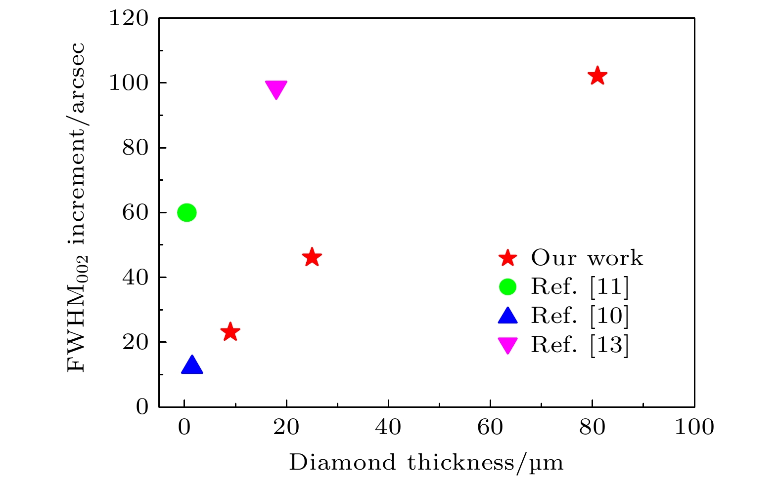
图 3 多晶金刚石厚度和XRD FWHM002增量统计结果
Fig. 3. Statistical results of polycrystalline diamond thickness and XRD FWHM002 increment.
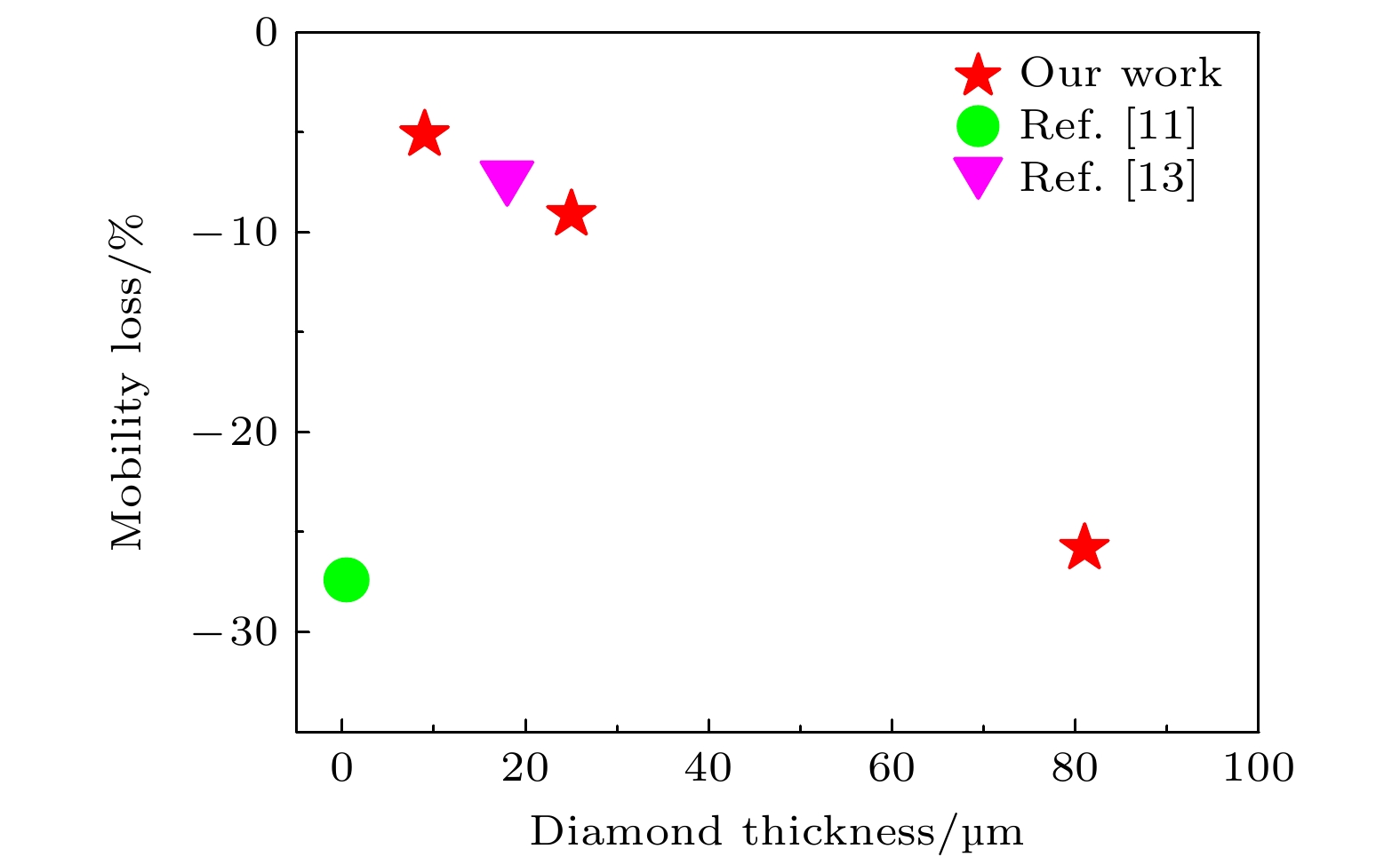
图 4 多晶金刚石厚度和GaN电性能衰退统计结果
Fig. 4. Statistical results of polycrystalline diamond thickness and mobility loss of GaN.

图 5 酸腐蚀后的Si基GaN材料表面SEM测试结果 (a) 放大1000倍; (b) 放大20000倍
Fig. 5. SEM measurement results of the surface of Si-based GaN material after acid etching: (a) Magnified 1000 times; (b) magnified 20000 times.
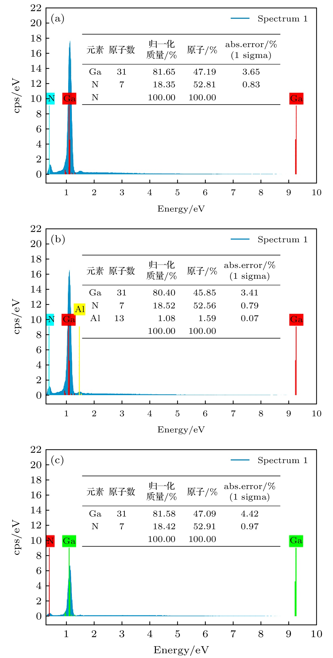
图 6 酸腐蚀后的Si基GaN材料表面3种区域EDS测试结果 (a) 平坦区域; (b) 裂纹区域; (c) 孔洞区域
Fig. 6. EDS results of three regions on the surface of Si-based GaN material after acid etching: (a) Flat region; (b) crack region; (c) hole region.

图 7 Si基GaN材料结构示意图
Fig. 7. Schematic diagram of sample structure of Si-based GaN material.
表 1 #3样品生长金刚石前/后、与金刚石剥离后的Raman, XRD和非接触霍尔测试结果
Table 1. Raman, XRD and Hall results for the #3 sample with the state of GaN/Si, Diamond/GaN/Si, and Exfoliated-GaN/Si.
测试参量 GaN/Si Diamond/GaN/Si Exfoliated-GaN/Si GaN peak/cm–1 568.1 567.8 568.1 FWHM002/arcsec 550 654 530 μ/(cm2·V–1·s–1) 1588.8 1178.2 1583.8 Ns/(electron, 1012 cm–2) 9.208 12.92 8.803 Rs/(Ω·square–1) 391.8 370.8 418.5  下载: 导出CSV
-
[1] EI Fatimy A, Dyakonova N, Meziani Y, Otsuji T, Knap W, Vandenbrouk S, Madjour K, Théron D, Gaquiere C, Poisson M A, Delage S, Prystawko P, Skierbiszewski C 2010 J. Appl. Phys. 107 024504
Google Scholar
[2] Marti D, Tirelli S, Alt A R, Roberts J, Bolognesi C R 2012 IEEE Electron Dev. Lett. 33 1372
Google Scholar
[3] Nazari M, Hancock B L, Piner E L, Holtz M W 2015 IEEE Compd. Semicond. Integr. Circuit Symp. 62 1467
Google Scholar
[4] Coe S E, Sussmann R S 2000 Diamond Relat. Mater. 9 1726
Google Scholar
[5] Alomari M, Dipalo M, Rossi S, Diforte-Poisson M A, Delage S, Carlin J F, Grandjean N, Gaquiere C, Toth L, Pecz B, Kohn E 2011 Diamond Relat. Mater. 20 604
Google Scholar
[6] Altman D, Tyhach M, McClymonds J, Kim S, Graham S 2014 Fourteenth Intersociety Conference on Thermal and Thermomechanical Phenomena in Electronic Systems (ITherm) Orlando, USA, May 27–30, 2014 p1199
[7] Anderson T J, Hobart K D, Tadjer M J, Koehler A D, Imhoff E A, Hite J K, Feygelson T I, Pate B B, Eddy Jr C R, Kub F J 2017 ECS J. Solid State Sci. Technol. 6 Q3036
Google Scholar
[8] Hancock B L, Nazari M, Anderson J, Piner E, Faili F, Oh S, Twitchen D, Graham S, Holtz M 2016 Appl. Phys. Lett. 108 211901
Google Scholar
[9] Zhou Y, Ramaneti R, Anaya J, Korneychuk S, Derluyn J, Sun H, Pomeroy J, Verbeeck J, Haenen K, Kubal M 2017 Appl. Phys. Lett. 111 041901
Google Scholar
[10] Ahmed R, Siddique A, Anderson J, Engdahl C, Holtz M, Piner E 2019 Cryst. Growth Des. 19 672
Google Scholar
[11] Siddique A, Ahmed R, Anderson J, Nazari M, Yates L, Graham S, Holtz M, Piner E L 2019 ACS Appl. Electron. Mater. 1 1387
Google Scholar
[12] Malakoutian M, Ren C H, Woo K, Li H, Chowdhury S 2021 Cryst. Growth Des. 21 2624
Google Scholar
[13] 杨士奇, 任泽阳, 张金风, 何琦, 苏凯, 张进成, 郭怀新, 郝跃 2021 固体电子学研究与进展 41 18
Google Scholar
Yang S Q, Ren Z Y, Zhang J F, He Q, Su K, Zhang J C, Guo H X, Hao Y 2021 Res. Prog. SSE 41 18
Google Scholar
[14] Wang A, Tadjer M J, Anderson T J, Baranyai R, Pomer J W 2013 IEEE Trans. Electron Dev. 60 3149
Google Scholar
[15] Tadjer M J, Anderson T J, Hobart K D, Mastro M A, Hite J K, Caldwell J D, Picard Y N, Kub F J, Eddy Jr C R 2010 Electron. Mater. 39 2452
Google Scholar
[16] Sun H, Simon R B P, Pomeroy J W, Francis D, Faili F, Twitchen D J, Kuball M 2015 Appl. Phys. Lett. 106 111906
Google Scholar
[17] Teng Y, Liu D Y, Tang K, Zhao W K, Chen Z A, Huang Y M, Duan J J, Bian Y, Ye J D, Zhu S M, Zhang R, Zheng Y D, Gu S M 2022 Chin. Phys. B 31 128106
Google Scholar
[18] 李俊鹏, 任泽阳, 张金风, 王晗雪, 马源辰, 费一帆, 黄思源, 丁森川, 张进成, 郝跃 2023 物理学报 72 038102
Google Scholar
Li J P, Ren Z Y, Zhang J F, Wang H X, Ma Y C, Fei Y F, Huang S Y, Ding S C, Zhang J C, Hao Y 2023 Acta Phys. Sin. 72 038102
Google Scholar
[19] Sein H, Ahmed W, Jackson M, Ali N, Gracio J 2003 Surf. Coat. Tech. 163 196
Google Scholar
[20] Xie W L, Lv X Y, Wang Q L, Li L A, Zou G T 2022 Chin. Phys. B 31 108106
Google Scholar
[21] Letts E, Key D, Hashimoto T 2016 J. Cryst. Growth 456 27
Google Scholar
[22] Davis R F, Gehrke T, Linthicum K J, Preble E, Rajagopal P, Ronning C, Zorman C, Mehregany M 2001 J. Cryst. Growth 231 335
Google Scholar
[23] Dadgar A, Schulze F, Wienecke M, Gadanecz A, Bläsing J, Veit P, Hempel T, Diez A, Christen J, Krost A 2007 New J. Phys. 9 389
Google Scholar
[24] Kumar M S, Kumar J 2003 Mater. Chem. Phys. 77 341
Google Scholar
[25] Sochacki T, Bryan Z, Amilusik M, Collazo R, Lucznik B, Weyher J L, Nowak G, Sadovyi B, Kamler G, Kucharski R 2013 Appl. Phys. Express 6 075504
Google Scholar
[26] Ahmed R, Siddique A, Anderson J, Gautam C, Holtz M, Piner E 2020 ACS Appl. Mater. Interfaces 12 39397
Google Scholar
[27] Cuenca J A, Smith M D, Field D E, Massabuau F C-P, Mandal S, Pomeroy J, Wallis D J, Oliver R A, Thayne I, Kuball M, Williams O A 2021 Carbon 174 647
Google Scholar
[28] Kisielowski C, Krüger J, Ruvimov S, Suski T, Ager J W, Jones E, Liliental-Weber Z, Rubin M, Weber E R, Bremser M D, Davis R F 1996 Phys. Rev. B Condens. Matter Mater. Phys. 54 17745
Google Scholar
[29] Kang B S, Kim S, Kim J, Ren F, Baik K, Pearton S J, Gila B P, Abernathy C R, Pan C C, Chen G T, Chyi J I, Chandrasekaran V, Sheplak M, Nishida T, Chu S N G 2003 Appl. Phys. Lett. 83 4845
Google Scholar
[30] Vanko G, Drzik M, Vallo M, Lalinsky T, Kutis V, Stancik S, Ryger I, Bencurova A 2011 Sens. Actuators A Phys. 172 1
Google Scholar
[31] Liu Y, Ruden P P, Xie J, Morkoc H, Son K A 2006 Appl. Phys. Lett. 88 013505
Google Scholar
[32] Azize M, Palacios T 2010 J. Appl. Phys. 108 023707
Google Scholar
[33] Jeon C M, Lee J L 2005 Appl. Phys. Lett. 86 172101
Google Scholar

 下载:
下载:
计量
- 文章访问数: 7480
- PDF下载量: 210
- 被引次数: 0
