-
磁隧道结是研究磁性材料自旋结构、输运特性、磁相变和磁各向异性的重要实验平台. 本研究基于干法转移技术制备了以机械剥离的少层范德瓦耳斯反铁磁绝缘体三氯化铬(CrCl3)为势垒层、少层石墨烯为电极的磁隧道结原型器件结构, 并进行了低温电磁输运测量, 除观测到自旋过滤效应引起的隧穿磁阻外, 还发现多种由非传统效应引起的磁阻变化. 基于对隧道结自旋结构和能带结构的分析, 本文将之归因于由磁近邻效应引起的隧穿机制改变, 以及石墨烯电极态密度在高磁场下出现的量子振荡行为. 本文报道了在二维磁隧道结中与隧穿磁阻相关且此前未被广泛关注的物理现象, 加深了对此类二维异质结构中载流子输运特性的理解, 为二维磁性材料的物理性质研究及其自旋电子学应用拓展了新的途径.
Magnetic tunnel junctions (MTJs) serve as essential platforms for investigating spin transport properties, magnetic phase transitions, and anisotropy in magnetic materials. Recently two-dimensional van der Waals antiferromagnetic insulators like chromium chloride (CrCl3) or chromium iodide (CrI3) have been used to develop spin-filtering magnetic tunnel junctions (sf-MTJs), improving the device performance for material property exploration and spintronic applications. However, it is crucial to recognize that the spin-filtering effect is not the sole determining factor of tunneling magnetoresistance (TMR) in these junctions; the interface magnetic exchange interactions and adjustable electrode density of states (DOS) fluctuations, response to applied electric or magnetic fields, can also influence the tunneling current. In this study, we fabricate MTJ devices by using mechanically-exfoliated few-layer CrCl3 as the tunnel barrier and few-layer graphene (FLG) as electrodes through dry transfer technique. Conducting low-temperature quantum transport measurements, we observe unconventional TMR behaviors, including bias-voltage-dependent TMR, oscillatory tunneling current under high magnetic fields, and tunable tunneling current via gate voltage. A qualitative model of elastic tunneling current is employed to analyze the spin and band characteristics of the MTJ device. The observed bias-voltage-dependent TMR is attributed to the changes in the tunneling mechanism due to magnetic proximity effect, which induces magnetization in the FLG electrode near the FLG/CrCl3 interface. The antiparallel alignment of polarized spin to CrCl3’s magnetization results in injected charge carriers facing a higher tunnel barrier, leading to negative TMR at lower bias voltages. As the bias voltage increases, the magnetic proximity effect lessens, and the device reverts to its conventional spin-filtering functionality. The oscillatory tunneling current is explained by the graphene electrode’s quantum oscillatory density of states behavior under vertical magnetic fields, which can be controlled by the applied gate voltage. This study contributes to the understanding of previously unexplored TMR phenomena in two-dimensional MTJs, deepening our insights into carrier transport properties in these heterostructures and broadening avenues for investigating the physical properties of two-dimensional magnetic materials and their spintronic applications. -
Keywords:
- magnetic tunnel junction /
- CrCl3 /
- negative tunneling magneto-resistance /
- gate tunability
[1] Geim A K, Grigorieva I V 2013 Nature 499 419
 Google Scholar
[2] Moodera J S, Kinder L R, Wong T M, Meservey R 1995 Phys. Rev. Lett. 74 3273
 Google Scholar
[3] Worledge D C, Geballe T H 2000 J. Appl. Phys. 88 5277
 Google Scholar
[4] Cai X H, Song T C, Wilson N P, Clark G, He M H, Zhang X O, Taniguchi T, Watanabe K, Yao W, Xiao D, McGuire M A, Cobden D H, Xu X D 2019 Nano Lett. 19 3993
 Google Scholar
[5] Song T C, Cai X H, Tu M W Y, Zhang X O, Huang B, Wilson N P, Seyler K L, Zhu L, Taniguchi T, Watanabe K, McGuire M A, Cobden D H, Xiao D, Yao W, Xu X D 2018 Science 360 1214
 Google Scholar
[6] Zeng X, Ye G, Huang S, Ye Q, Li W, Chen C, Kuang H, Li M, Liu Y, Pan Z, Hasan T, Luo J, Lu X, Wang X 2022 Nano Today 42 101373
 Google Scholar
[7] Zatko V, Dubois S M M, Godel F, Galbiati M, Peiro J, Sander A, Carretero C, Vecchiola A, Collin S, Bouzehouane K, Servet B, Petroff F, Charlier J C, Martin M B, Dlubak B, Seneor P 2022 ACS Nano 16 14007
 Google Scholar
[8] Jiang S W, Li L Z, Wang Z F, Mak K F, Shan J 2018 Nat. Nanotechnol. 13 549
 Google Scholar
[9] Zhang Y B, Tan Y W, Stormer H L, Kim P 2005 Nature 438 201
 Google Scholar
[10] Zhang Y B, Small J P, Amori M E S, Kim P 2005 Phys. Rev. Lett. 94 176803
 Google Scholar
[11] Li G H, Andrei E Y 2007 Nat. Phys. 3 623
 Google Scholar
[12] McGuire M A, Clark G, KC S, Chance W M, Jellison G E, Cooper V R, Xu X D, Sales B C 2017 Phys. Rev. Mater. 1 014001
 Google Scholar
[13] Zhu R, Zhang W, Shen W, Wong P K J, Wang Q, Liang Q, Tian Z, Zhai Y, Qiu C W, Wee A T S 2020 Nano Lett. 20 5030
 Google Scholar
[14] Tseng C C, Song T, Jiang Q, Lin Z, Wang C, Suh J, Watanabe K, Taniguchi T, McGuire M A, Xiao D, Chu J H, Cobden D H, Xu X, Yankowitz M 2022 Nano Lett. 22 8495
 Google Scholar
[15] Jiang D, Yuan T Z, Wu Y Z, Wei X Y, Mu G, An Z H, Li W 2020 ACS Appl. Mater. Interfaces 12 49252
 Google Scholar
[16] Liu Y, Petrovic C 2020 Phys. Rev. B 102 014424
 Google Scholar
[17] Sun W, Wang W X, Zang J D, Li H, Zhang G B, Wang J L, Cheng Z X 2021 Adv. Funct. Mater. 31 2104452
 Google Scholar
[18] Zomer P J, Guimarães M H D, Brant J C, Tombros N, van Wees B J 2014 Appl. Phys. Lett. 105 013101
 Google Scholar
[19] Wang Z, Gibertini M, Dumcenco D, Taniguchi T, Watanabe K, Giannini E, Morpurgo A F 2019 Nat. Nanotechnol. 14 1116
 Google Scholar
[20] Wang Z, Gutiérrez-Lezama I, Ubrig N, Kroner M, Gibertini M, Taniguchi T, Watanabe K, Imamoğlu A, Giannini E, Morpurgo A F 2018 Nat. Commun. 9 2516
 Google Scholar
[21] Klein D R, MacNeill D, Song Q, Larson D T, Fang S, Xu M, Ribeiro R A, Canfield P C, Kaxiras E, Comin R, Jarillo-Herrero P 2019 Nat. Phys. 15 1255
 Google Scholar
[22] Liehr M, Hazra J, Beckmann K, Mukundan V, Alexandrou I, Yeow T, Race J, Tapily K, Consiglio S, Kurinec S K, Diebold A C, Cady N 2023 J. Vac. Sci. Technol. B 41 012805
 Google Scholar
[23] Wang J, Ahmadi Z, Lujan D, Choe J, Taniguchi T, Watanabe K, Li X, Shield J E, Hong X 2023 Adv. Sci. 10 2203548
 Google Scholar
[24] Ghiasi T S, Kaverzin A A, Dismukes A H, de Wal D K, Roy X, van Wees B J 2021 Nat. Nanotechnol. 16 788
 Google Scholar
[25] Jeong J, Kiem D H, Guo D, Duan R, Watanabe K, Taniguchi T, Liu Z, Han M J, Zheng S, Yang H 2024 Adv. Mater. 36 2310291
 Google Scholar
[26] Wu Y F, Cui Q R, Zhu M Y, Liu X J, Wang Y, Zhang J Y, Zheng X Q, Shen J X, Cui P, Yang H X, Wang S G 2021 ACS Appl. Mater. Interfaces 13 10656
 Google Scholar
[27] Britnell L, Gorbachev R V, Jalil R, Belle B D, Schedin F, Mishchenko A, Georgiou T, Katsnelson M I, Eaves L, Morozov S V, Peres N M R, Leist J, Geim A K, Novoselov K S, Ponomarenko L A 2012 Science 335 947
 Google Scholar
[28] Xie B H, Ji Z J, Wu J X, Zhang R, Jin Y M, Watanabe K, Taniguchi T, Liu Z, Cai X H 2023 ACS Nano 17 18352
 Google Scholar
[29] McClure J W 1957 Phys. Rev. 108 612
 Google Scholar
-
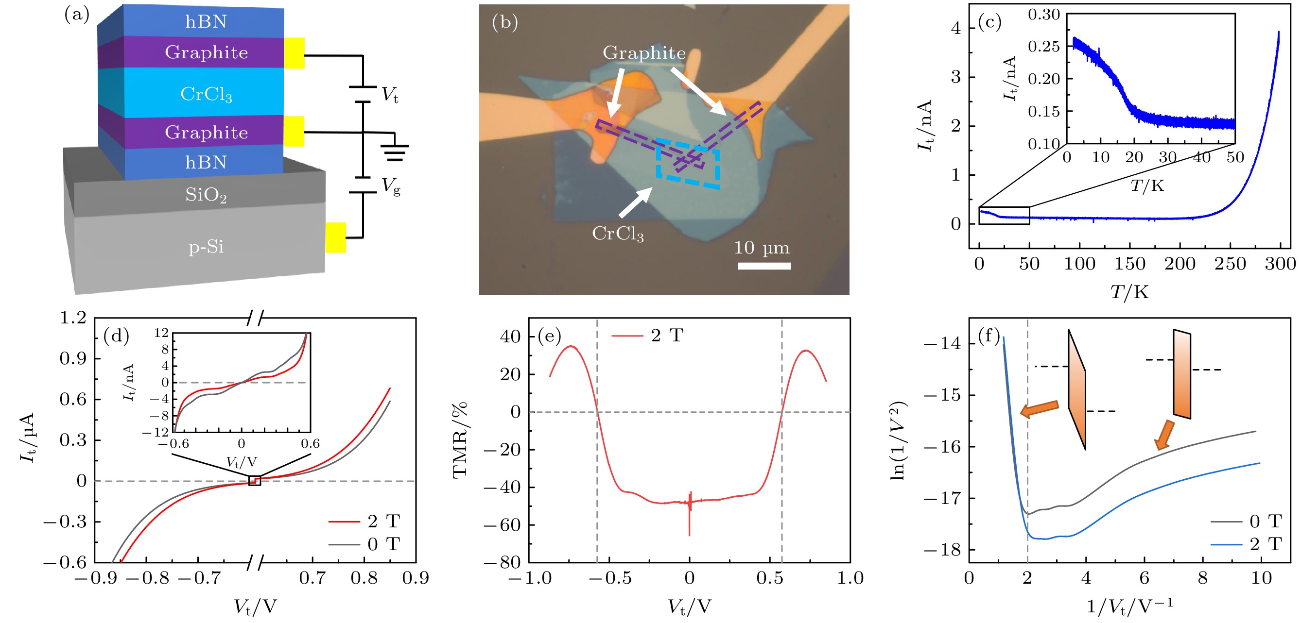
图 1 器件的电输运表征测试 (a)器件结构示意图; (b)器件光学显微照片, 其中石墨电极和CrCl3的位置使用虚线框示意标出; (c)隧穿电流随温度的变化, 插图是对2—50 K区域的放大; (d)低温伏安特性曲线, 插图是对–0.6—0.6 V区域的放大; (e)根据图(d)计算的隧穿磁阻曲线; (f)根据图(d)计算的F-N图, 插图为两种隧穿机制下的能带图
Fig. 1. Transport characterizations of the device: (a) Schematic of the device, with the positions of the graphite electrodes and CrCl3 indicated by dashed boxes; (b) optical micrograph of the device; (c) tunneling current as a function of the temperature. Inset: zoom-in plot of the range between 2–50 K; (d) low-temperature I-V characteristic, inset: zoom-in plot of the range between –0.6–0.6 V; (e) TMR as a function of the bias voltage derived from (d); (f) F-N plot derived from panel (d), insets are band diagram under two tunneling regimes.
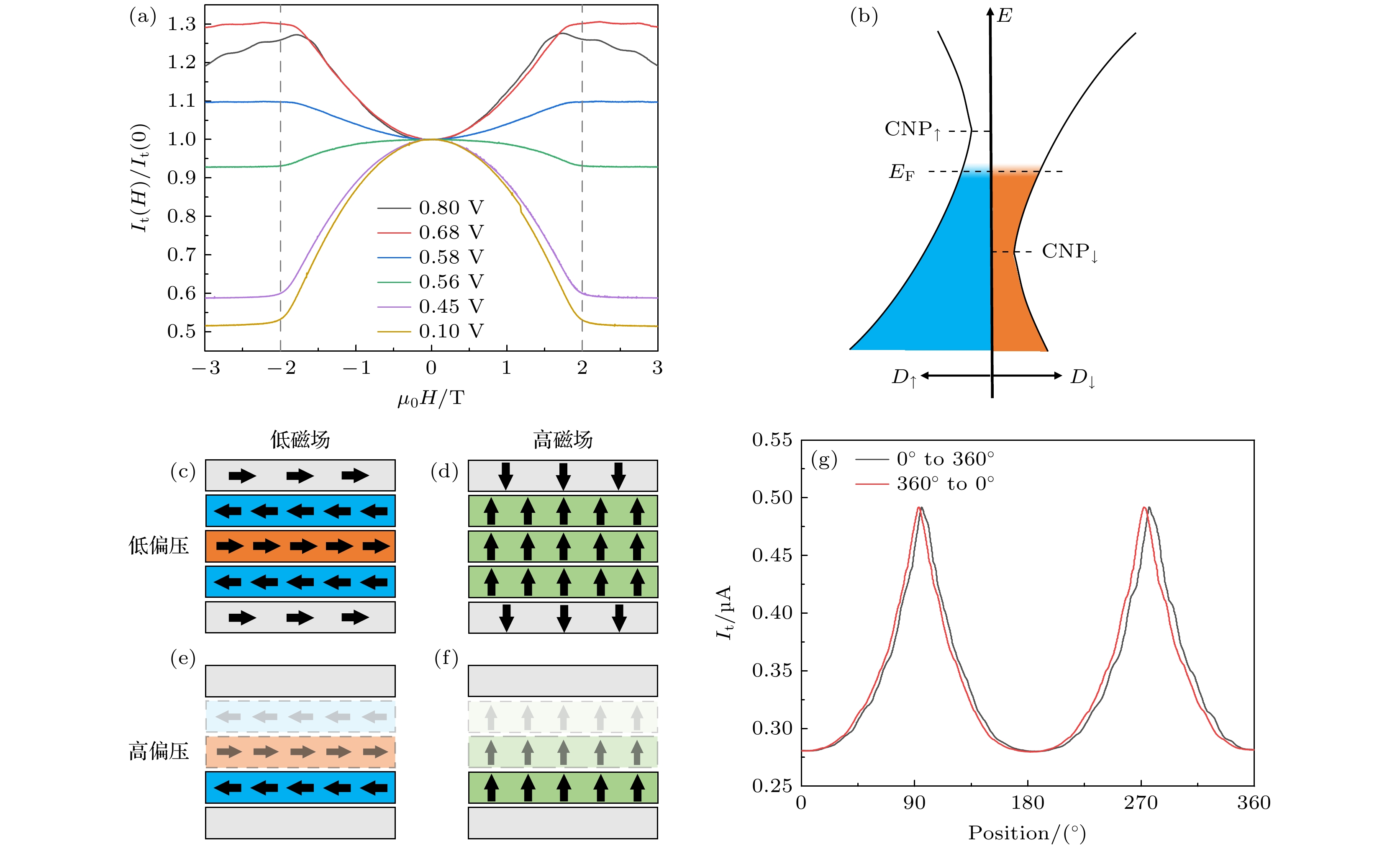
图 2 对器件TMR特性的实验和理论解释 (a)不同偏置电压下的归一化隧穿电流曲线; (b)石墨电极态密度的自旋劈裂示意图, 着色区域表示电子布居数. (c)—(f)磁隧道结自旋结构示意图, 分别对应(c)低偏压、低磁场, (d)低偏压、高磁场, (e)高偏压、低磁场, (f)高偏压、高磁场. (g)隧穿电流随磁场方向与样品法向夹角的变化
Fig. 2. Experimental and theoretical explanation of TMR characteristics of the device: (a) Normalized tunneling current as a function of the out-of-plane magnetic field under different dc bias voltages; (b) schematic of spin splitting of graphite’s DOS, with the shaded area representing population of electrons. (c)–(f) Schematics of spin configuration of the MTJ, with each plot corresponding to the regime of (c) low bias, low magnetic field, (d) low bias, high magnetic field, (e) high bias, low magnetic field and (f) high bias, high magnetic field, respectively. (g) Tunneling current as a function of the angle between the magnetic field and the normal direction of the sample.
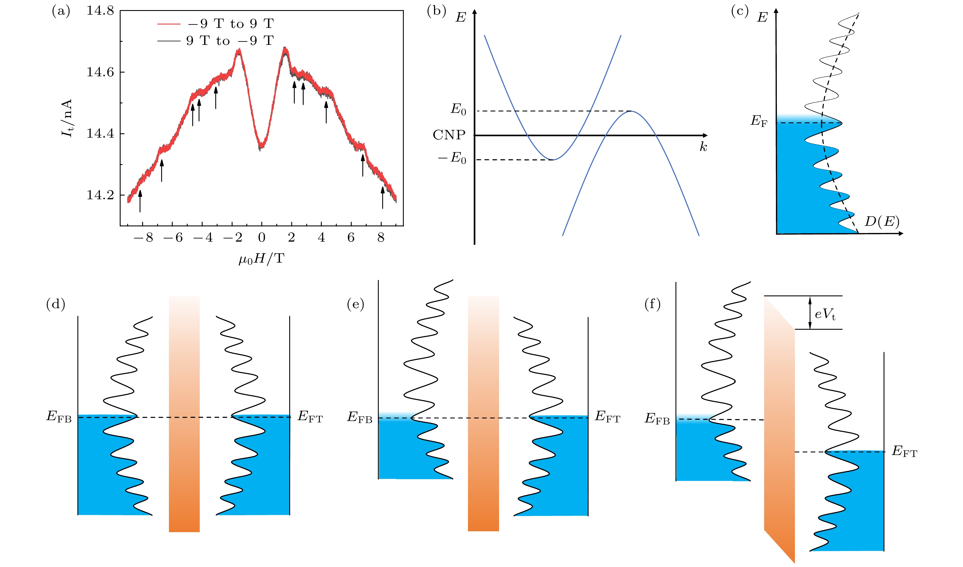
图 3 隧穿电流的量子振荡 (a)隧穿电流随竖直方向磁场的变化关系曲线, 测试在T = 2 K下进行; (b)少层石墨烯能带的STB模型; (c)少层石墨烯态密度发生部分量子化的示意图. (d)—(f) MTJ器件的能带图(EFB和EFT分别代表底电极和顶电极的费米能级) (d)热平衡情况; (e)施加一定负栅极电压的情况; (f)同时施加负栅极电压和正向偏置电压的情况
Fig. 3. Quantum oscillation of the tunneling current: (a) Tunneling current as a function of the out-of-plane magnetic field, at the temperature of T = 2 K; (b) STB model showing the band structure of few-layer graphene; (c) schematic of partial quantization of DOS in few-layer graphene. (d)–(f) Band structures of MTJ device (EFB and EFT represents the Fermi level of bottom and top graphite electrode, respectively): (d) in thermal equilibrium; (e) with an applied negative gate voltage; (f) with both an applied negative gate voltage and a positive bias voltage, respectively.
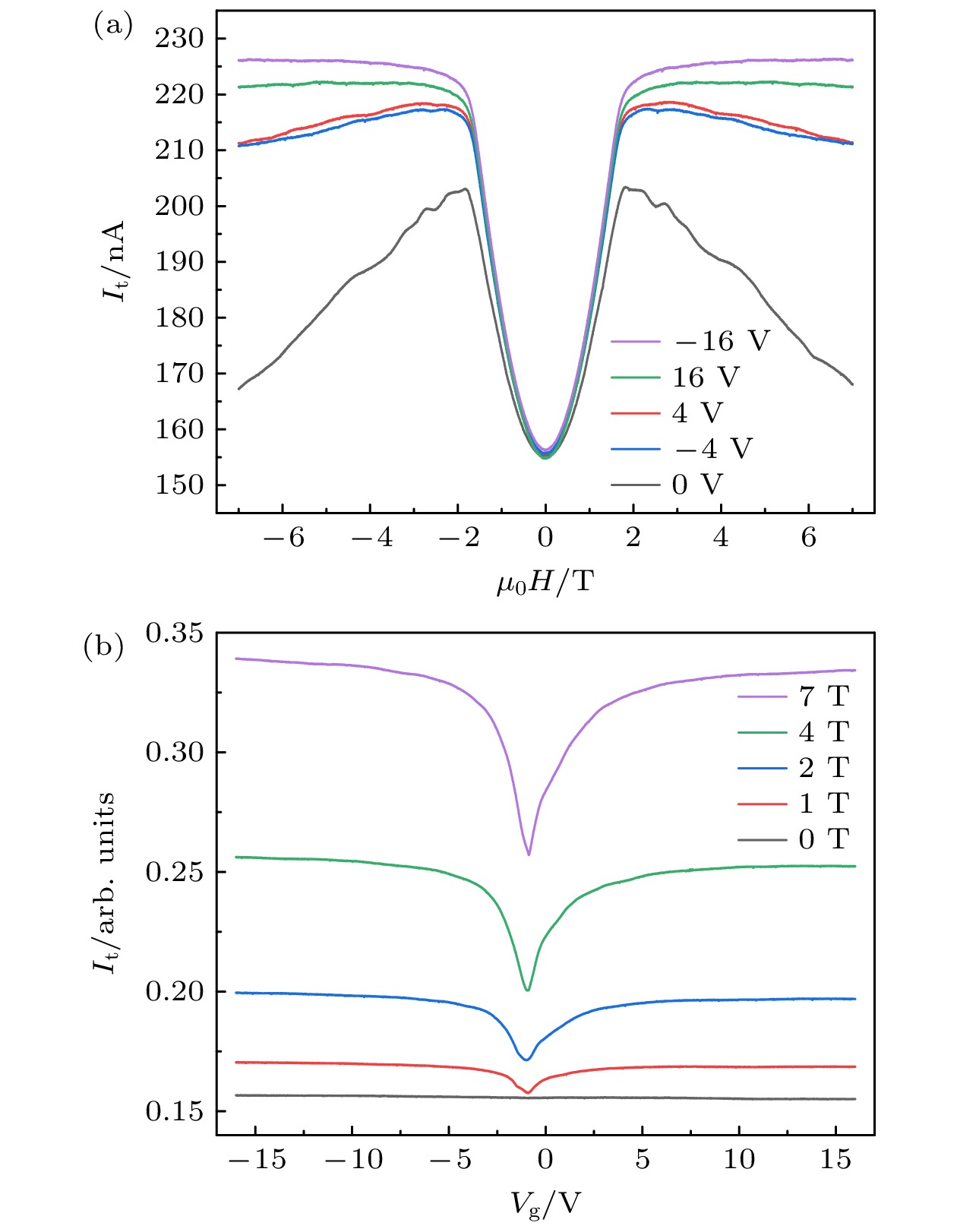
图 4 隧穿电流的栅极电压依赖性 (a)不同栅极电压下隧穿电流随磁场的变化关系; (b)不同磁场下器件的转移特性, 所有测试在T = 2 K下进行
Fig. 4. Gate dependence of the tunneling current: (a) Tunneling current as a function of the out-of-plane magnetic field with different applied gate voltages; (b) transfer characteristics of the device at selected out-of-plane magnetic fields, all measurements are carried out at the temperature T = 2 K.
-
[1] Geim A K, Grigorieva I V 2013 Nature 499 419
 Google Scholar
[2] Moodera J S, Kinder L R, Wong T M, Meservey R 1995 Phys. Rev. Lett. 74 3273
 Google Scholar
[3] Worledge D C, Geballe T H 2000 J. Appl. Phys. 88 5277
 Google Scholar
[4] Cai X H, Song T C, Wilson N P, Clark G, He M H, Zhang X O, Taniguchi T, Watanabe K, Yao W, Xiao D, McGuire M A, Cobden D H, Xu X D 2019 Nano Lett. 19 3993
 Google Scholar
[5] Song T C, Cai X H, Tu M W Y, Zhang X O, Huang B, Wilson N P, Seyler K L, Zhu L, Taniguchi T, Watanabe K, McGuire M A, Cobden D H, Xiao D, Yao W, Xu X D 2018 Science 360 1214
 Google Scholar
[6] Zeng X, Ye G, Huang S, Ye Q, Li W, Chen C, Kuang H, Li M, Liu Y, Pan Z, Hasan T, Luo J, Lu X, Wang X 2022 Nano Today 42 101373
 Google Scholar
[7] Zatko V, Dubois S M M, Godel F, Galbiati M, Peiro J, Sander A, Carretero C, Vecchiola A, Collin S, Bouzehouane K, Servet B, Petroff F, Charlier J C, Martin M B, Dlubak B, Seneor P 2022 ACS Nano 16 14007
 Google Scholar
[8] Jiang S W, Li L Z, Wang Z F, Mak K F, Shan J 2018 Nat. Nanotechnol. 13 549
 Google Scholar
[9] Zhang Y B, Tan Y W, Stormer H L, Kim P 2005 Nature 438 201
 Google Scholar
[10] Zhang Y B, Small J P, Amori M E S, Kim P 2005 Phys. Rev. Lett. 94 176803
 Google Scholar
[11] Li G H, Andrei E Y 2007 Nat. Phys. 3 623
 Google Scholar
[12] McGuire M A, Clark G, KC S, Chance W M, Jellison G E, Cooper V R, Xu X D, Sales B C 2017 Phys. Rev. Mater. 1 014001
 Google Scholar
[13] Zhu R, Zhang W, Shen W, Wong P K J, Wang Q, Liang Q, Tian Z, Zhai Y, Qiu C W, Wee A T S 2020 Nano Lett. 20 5030
 Google Scholar
[14] Tseng C C, Song T, Jiang Q, Lin Z, Wang C, Suh J, Watanabe K, Taniguchi T, McGuire M A, Xiao D, Chu J H, Cobden D H, Xu X, Yankowitz M 2022 Nano Lett. 22 8495
 Google Scholar
[15] Jiang D, Yuan T Z, Wu Y Z, Wei X Y, Mu G, An Z H, Li W 2020 ACS Appl. Mater. Interfaces 12 49252
 Google Scholar
[16] Liu Y, Petrovic C 2020 Phys. Rev. B 102 014424
 Google Scholar
[17] Sun W, Wang W X, Zang J D, Li H, Zhang G B, Wang J L, Cheng Z X 2021 Adv. Funct. Mater. 31 2104452
 Google Scholar
[18] Zomer P J, Guimarães M H D, Brant J C, Tombros N, van Wees B J 2014 Appl. Phys. Lett. 105 013101
 Google Scholar
[19] Wang Z, Gibertini M, Dumcenco D, Taniguchi T, Watanabe K, Giannini E, Morpurgo A F 2019 Nat. Nanotechnol. 14 1116
 Google Scholar
[20] Wang Z, Gutiérrez-Lezama I, Ubrig N, Kroner M, Gibertini M, Taniguchi T, Watanabe K, Imamoğlu A, Giannini E, Morpurgo A F 2018 Nat. Commun. 9 2516
 Google Scholar
[21] Klein D R, MacNeill D, Song Q, Larson D T, Fang S, Xu M, Ribeiro R A, Canfield P C, Kaxiras E, Comin R, Jarillo-Herrero P 2019 Nat. Phys. 15 1255
 Google Scholar
[22] Liehr M, Hazra J, Beckmann K, Mukundan V, Alexandrou I, Yeow T, Race J, Tapily K, Consiglio S, Kurinec S K, Diebold A C, Cady N 2023 J. Vac. Sci. Technol. B 41 012805
 Google Scholar
[23] Wang J, Ahmadi Z, Lujan D, Choe J, Taniguchi T, Watanabe K, Li X, Shield J E, Hong X 2023 Adv. Sci. 10 2203548
 Google Scholar
[24] Ghiasi T S, Kaverzin A A, Dismukes A H, de Wal D K, Roy X, van Wees B J 2021 Nat. Nanotechnol. 16 788
 Google Scholar
[25] Jeong J, Kiem D H, Guo D, Duan R, Watanabe K, Taniguchi T, Liu Z, Han M J, Zheng S, Yang H 2024 Adv. Mater. 36 2310291
 Google Scholar
[26] Wu Y F, Cui Q R, Zhu M Y, Liu X J, Wang Y, Zhang J Y, Zheng X Q, Shen J X, Cui P, Yang H X, Wang S G 2021 ACS Appl. Mater. Interfaces 13 10656
 Google Scholar
[27] Britnell L, Gorbachev R V, Jalil R, Belle B D, Schedin F, Mishchenko A, Georgiou T, Katsnelson M I, Eaves L, Morozov S V, Peres N M R, Leist J, Geim A K, Novoselov K S, Ponomarenko L A 2012 Science 335 947
 Google Scholar
[28] Xie B H, Ji Z J, Wu J X, Zhang R, Jin Y M, Watanabe K, Taniguchi T, Liu Z, Cai X H 2023 ACS Nano 17 18352
 Google Scholar
[29] McClure J W 1957 Phys. Rev. 108 612
 Google Scholar
计量
- 文章访问数: 4842
- PDF下载量: 105
- 被引次数: 0


 下载:
下载:
