-
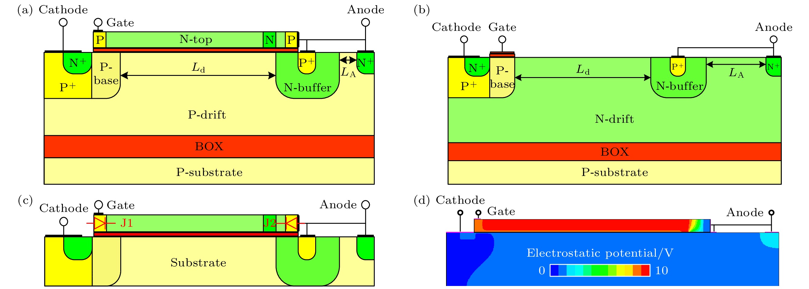
通过引入n+阳极在体内集成续流二极管的逆导型横向绝缘栅双极晶体管(reverse-conducting lateral insulated gate bipolar transistor, RC-LIGBT)可以实现反向导通, 并且优化器件的关断特性, 是功率集成电路中一个有竞争力的器件. 本文提出了一种新型载流子积累的RC-LIGBT, 它具有电子控制栅(electron-controlled gate, EG)和分离短路阳极(separated short-anode, SSA), 可以同时实现较低的导通压降和关断损耗. 在正向导通状态, 漂移区上方的EG结构可以在漂移区的表面积累一个高密度的电子层, 从而大大地降低器件的导通压降. 同时, SSA结构的使用还极大优化了器件的关断损耗. 另外, 低掺杂p型漂移区与SSA结构配合, 可以简单地实现反向导通并且消除回吸电压. 仿真结果表明, 所提出的器件具有优秀的导通压降与关断损耗之间的折衷关系, 其导通压降为1.16 V, 比SSA LIGBT低55%, 其关断损耗为0.099 mJ/cm2, 比SSA LIGBT和常规LIGBT分别低38.5%和94.7%.
-
关键词:
- 载流子积累 /
- 逆导型横向绝缘栅双极晶体管 /
- 导通压降 /
- 回吸电压
Reverse-conducting lateral insulated gate bipolar transistor (RC-LIGBT) with freewheeling diode integrated in the body by introducing n+ anode can realize the reverse conduction and optimize the turn-off characteristics of the device, which is a promising device in a power integrated circuit. In this work, a novel RC-LIGBT with electron-controlled gate (EG) and separated short-anode (SSA) is proposed and investigated by TCAD simulation, which can achieve low on-state voltage drop (Von) and low turn-off loss (Eoff) at the same time. The EG structure of p-n-n+-p (p+ region/n-type silicon region/n-type barrier layer/p+ region) is adopted, the gate electrode and anode electrode are connected by the EG structure. In the forward conduction state, a high-density electron accumulation layer is formed on the surface of the drift region by EG structure, which greatly reduces the Von of the device. At the same time, the use of the SSA structure can also optimize the Eoff of the device by forming an additional electron extraction channel. In addition, based on the EG structure, a low-doping p-drift can be combined with the SSA structure to simply achieve reverse-conduction and snapback-free characteristics. Furthermore, the EG structure and the SSA structure can complement each other. On the one hand, the high-density electron accumulation layer formed by EG structure compensates for the weakened conductance modulation effect caused by the SSA structure. On the other hand, the electron extraction channel of the SSA structure enables a large number of accumulated electrons to be removed quickly. The simulation results show that the proposed device has an excellent trade-off relationship between Von and Eoff, specifically, Von is 1.16V, which is 55% lower than that of SSA LIGBT, and Eoff is 0.099 mJ/cm2, which is 38.5% and 94.7% lower than that of SSA LIGBT and conventional LIGBT, respectively.-
Keywords:
- carrier accumulation /
- reverse-conducting lateral insulated gate bipolar transistor /
- on-state voltage drop /
- snapback voltage
[1] Sakurai N, Mori M, Yatsuo T 1990 Proceedings of the 2nd International Symposium on Power Semiconductor Devices and ICs Tokyo, Japan, April 4–6, 1990 p66
[2] Disney D, Letavic T, Trajkovic T, Terashima T, Nakagawa A 2017 IEEE T. Electron Dev. 64 659
 Google Scholar
[3] Letavic T, Petruzzello J, Claes J, Eggenkamp P, Janssen E, van der Wal A 2006 IEEE International Symposium on Power Semiconductor Devices and IC's Naples, Italy, June 4–8, 2006 p1
[4] Gu Y, Ma J, Zhang L, Wei J X, Li S, Liu S Y, Zhang S, Zhu J, Sun W F 2024 IEEE T. Electron Dev. 71 381
 Google Scholar
[5] Hara K, Wada S, Sakano J, Oda T, Sakurai K, Yamashita H, Utsumi T 2014 IEEE 26th International Symposium on Power Semiconductor Devices & IC's Waikoloa, Hawaii, USA, June 15–19, 2014 p418
[6] Gough P A, Simpson M R, Rumennik V 1986 International Electron Devices Meeting Los Angeles, CA, USA, December 7–10, 1986 p218
[7] Sin J K O, Mukherjee S 1991 IEEE Electron Dev. Lett. 12 45
 Google Scholar
[8] Duan S, Qiao M, Mao K, Zhong B, Jiang L, Zhang B 2010 IEEE International Conference on Solid-State and Integrated Circuit Technology Shanghai, China, November 1–4, 2010 p897
[9] Simpson M R 1991 IEEE T. Electron Dev. 38 1633
 Google Scholar
[10] Chen W S, Zhang B, Li Z J 2010 IEEE Electron Dev. Lett. 31 467
 Google Scholar
[11] Sun L C, Duan B X, Yang Y T 2021 IEEE T. Electron Dev. 68 2408
 Google Scholar
[12] Chul J H, Byeon D S, Oh J K, Han M K, Choi Proc Y I 2002 12th International Symposium on Power Semiconductor Devices & ICs Toulouse, France, May 22–25, 2002 p149
[13] Zhu J, Zhang L, Sun W F, Chen M, Zhou F, Zhao M N, Shi L X, Gu Y, Zhang S 2016 IEEE T. Electron Dev. 63 2003
 Google Scholar
[14] Huang L H, Luo X R, Wei J, Zhou K, Deng G Q, Sun T, Ouyang D F, Fan D, Zhang B 2017 IEEE T. Electron Dev. 64 3961
 Google Scholar
[15] Hardikar S, Tadikonda R, Sweet M, Vershinin K, Narayanan E M S 2003 IEEE Electron Dev. Lett. 24 701
 Google Scholar
[16] Sun L C, Duan B X, Wang Y D, Yang Y T 2019 IEEE T. Electron Dev. 66 2675
 Google Scholar
[17] Duan B X, Sun L C, Yang Y T 2019 IEEE Electron Dev. Lett. 40 63
 Google Scholar
[18] Liu S Y, Zhang Y, Zhang Z J, Inuishi M 2022 6th IEEE Electron Devices Technology & Manufacturing Conference Oita, Japan, March 6–9, 2022 p204
[19] Xia Y, Chen W J, Liu C, Sun R Z, Li Z J, Zhang B Zhang 2022 IEEE T. Electron Dev. 69 6956
 Google Scholar
[20] 夏庆锋 2007 硕士学位论文 (杭州: 浙江大学)
Xia Q F 2007 M. S. Thesis (Hangzhou: Zhejiang University
[21] Bruel M, Aspar B, Charlet B, Maleville C, Poumeyrol T, Soubie A, Auberton-Herve A J, Lamure J M, Barge T, Metral F, Trucchi S 1995 IEEE International SOI Conference Proceedings Tucson, AZ, USA, October 3–5, 1995 p178
-
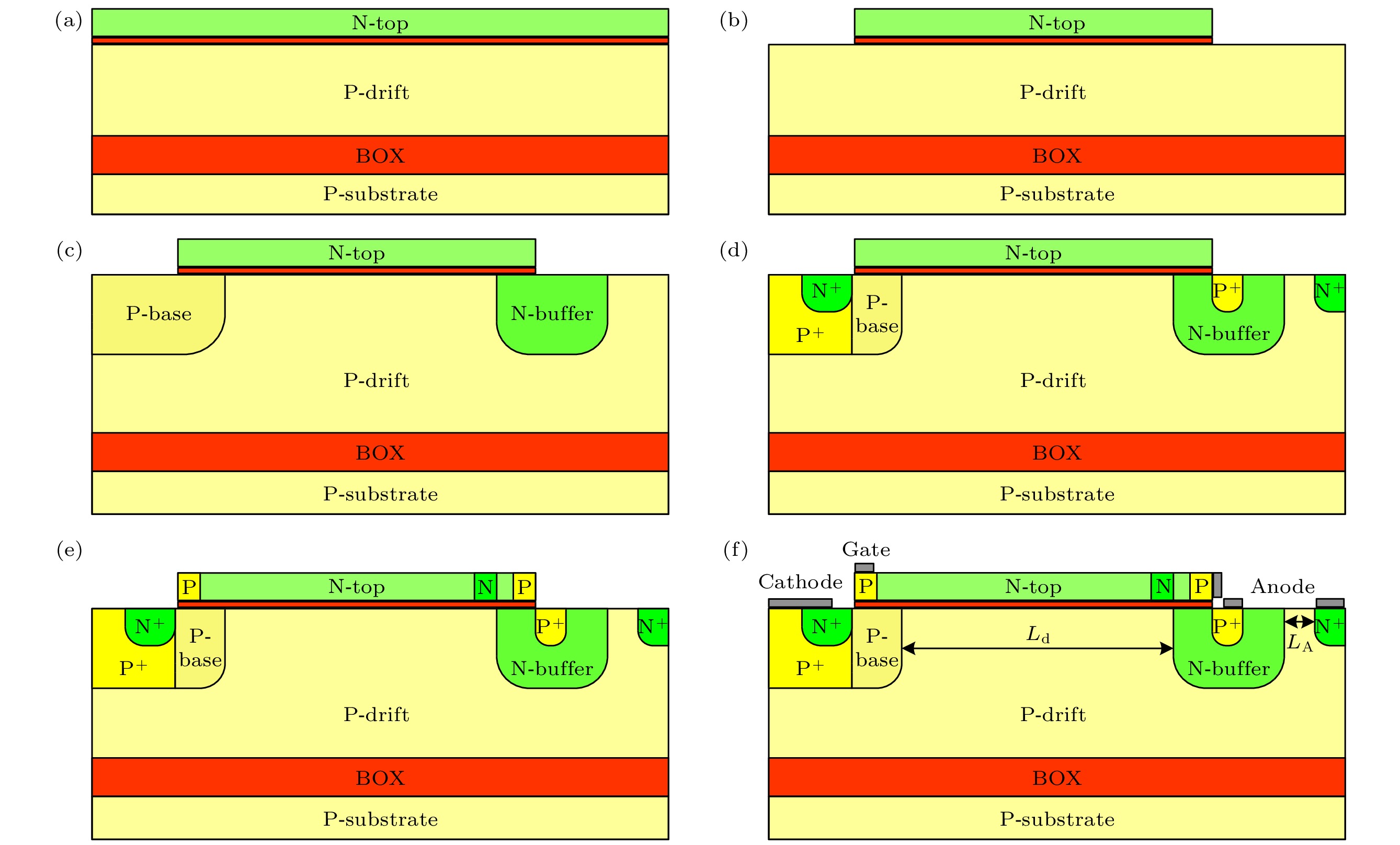
图 2 ES LIGBT的关键工艺流程图 (a)准备双层SOI晶圆; (b)刻蚀; (c)扩散形成P-base和N-buffer; (d)离子注入形成阳极结构和阴极结构; (e)对顶层硅进行离子注入; (f)金属化, 形成电极
Fig. 2. Key process flow to fabricate ES LIGBT: (a) Preparing the double SOI wafer; (b) etching; (c) diffusion to form P-base and N-buffer; (d) ion implantation to form an anode structure and a cathode structure; (e) ion implantation of the top layer silicon; (f) metallization to form electrodes.
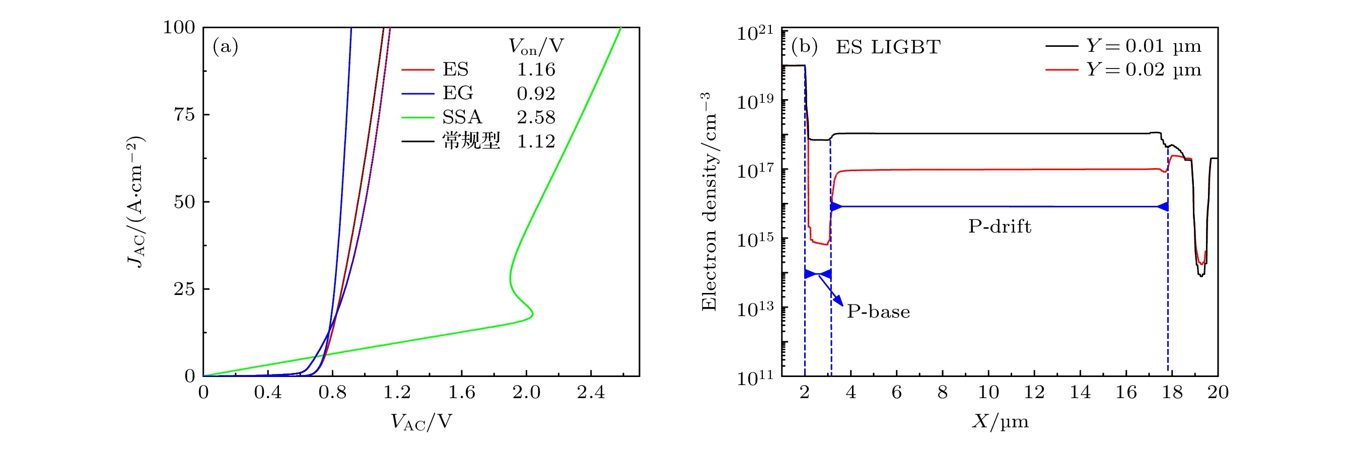
图 3 (a) LIGBT的击穿特性, 插图为击穿时所提出的ES LIGBT的总电流密度, 其中JAC是阳极电流密度, VAC是阳极和阴极之间的电压; (b) Ntop对ES LIGBT击穿电压的影响
Fig. 3. (a) Breakdown characteristics for LIGBTs. The inset is the total current density of the proposed ES LIGBT at the time of breakdown, JAC is the anode current density and VAC is the voltage between the anode and cathode. (b) Impact of Ntop on BV for the ES LIGBT.
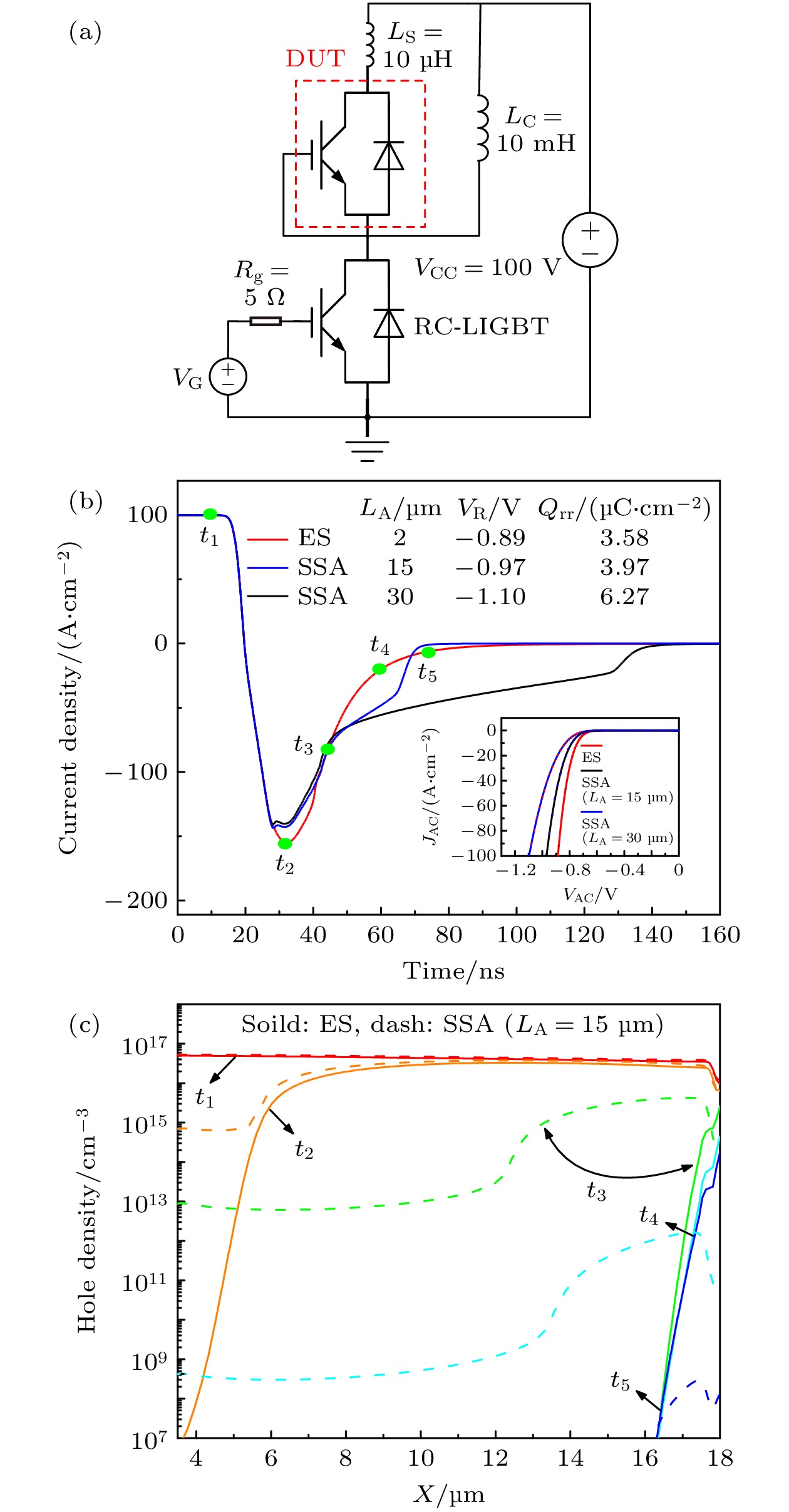
图 5 (a) 反向恢复特性的仿真测试, 其中VG是栅极电压, 栅极电阻RG = 10 Ω, 杂散电感Ls = 10 μH, 负载电感LC = 10 mH, 直流电源电压VCC = 100 V; (b) ES LIGBT和SSA LIGBTs的反向导通特性和反向恢复特性; (c) 反向恢复过程中不同时刻t1—t5的空穴密度分布
Fig. 5. (a) Simulation test circuit for reverse recovery characteristics, where VG is the gate voltage, gate resistance RG = 10 Ω, stray inductance Ls = 10 μH, load inductance LC = 10 mH, and dc power supply voltage VCC = 100 V; (b) RC and reverse recovery characteristics of ES LIGBT and SSA LIGBTs; (c) hole density distribution at different moment (t1–t5) of reverse recovery process.
表 1 仿真中的关键参数
Table 1. Key parameters used in simulation.
参数符号 参数含义 常规LIGBT SSA LIGBT ES LIGBT Ld/μm 漂移区长度 15 15 15 Tbox/μm 埋氧层厚度 3 3 3 Tox/nm 栅氧化层厚度 50 50 50 Tn/μm 漂移区厚度 4 4 4 LA/μm P+阳极和N+阳极间长度 — 15 2 Ttop/μm 顶层硅栅厚度 — — 1 Ndrift/(1014 cm–3) 漂移区掺杂浓度 18 18 1 Nsubstrate/(1014 cm–3) P型衬底掺杂浓度 1 1 1 Nbuffer/(1017 cm–3) N型缓冲层掺杂浓度 2 2 2 Np-anode/(1019 cm–3) P+阳极掺杂浓度 5 5 5 Ntop/(1015 cm–3) 顶层N型硅区掺杂浓度 — — 9.1 Nbarrier/(1018 cm–3) 顶层N型势垒层掺杂浓度 — — 5 -
[1] Sakurai N, Mori M, Yatsuo T 1990 Proceedings of the 2nd International Symposium on Power Semiconductor Devices and ICs Tokyo, Japan, April 4–6, 1990 p66
[2] Disney D, Letavic T, Trajkovic T, Terashima T, Nakagawa A 2017 IEEE T. Electron Dev. 64 659
 Google Scholar
[3] Letavic T, Petruzzello J, Claes J, Eggenkamp P, Janssen E, van der Wal A 2006 IEEE International Symposium on Power Semiconductor Devices and IC's Naples, Italy, June 4–8, 2006 p1
[4] Gu Y, Ma J, Zhang L, Wei J X, Li S, Liu S Y, Zhang S, Zhu J, Sun W F 2024 IEEE T. Electron Dev. 71 381
 Google Scholar
[5] Hara K, Wada S, Sakano J, Oda T, Sakurai K, Yamashita H, Utsumi T 2014 IEEE 26th International Symposium on Power Semiconductor Devices & IC's Waikoloa, Hawaii, USA, June 15–19, 2014 p418
[6] Gough P A, Simpson M R, Rumennik V 1986 International Electron Devices Meeting Los Angeles, CA, USA, December 7–10, 1986 p218
[7] Sin J K O, Mukherjee S 1991 IEEE Electron Dev. Lett. 12 45
 Google Scholar
[8] Duan S, Qiao M, Mao K, Zhong B, Jiang L, Zhang B 2010 IEEE International Conference on Solid-State and Integrated Circuit Technology Shanghai, China, November 1–4, 2010 p897
[9] Simpson M R 1991 IEEE T. Electron Dev. 38 1633
 Google Scholar
[10] Chen W S, Zhang B, Li Z J 2010 IEEE Electron Dev. Lett. 31 467
 Google Scholar
[11] Sun L C, Duan B X, Yang Y T 2021 IEEE T. Electron Dev. 68 2408
 Google Scholar
[12] Chul J H, Byeon D S, Oh J K, Han M K, Choi Proc Y I 2002 12th International Symposium on Power Semiconductor Devices & ICs Toulouse, France, May 22–25, 2002 p149
[13] Zhu J, Zhang L, Sun W F, Chen M, Zhou F, Zhao M N, Shi L X, Gu Y, Zhang S 2016 IEEE T. Electron Dev. 63 2003
 Google Scholar
[14] Huang L H, Luo X R, Wei J, Zhou K, Deng G Q, Sun T, Ouyang D F, Fan D, Zhang B 2017 IEEE T. Electron Dev. 64 3961
 Google Scholar
[15] Hardikar S, Tadikonda R, Sweet M, Vershinin K, Narayanan E M S 2003 IEEE Electron Dev. Lett. 24 701
 Google Scholar
[16] Sun L C, Duan B X, Wang Y D, Yang Y T 2019 IEEE T. Electron Dev. 66 2675
 Google Scholar
[17] Duan B X, Sun L C, Yang Y T 2019 IEEE Electron Dev. Lett. 40 63
 Google Scholar
[18] Liu S Y, Zhang Y, Zhang Z J, Inuishi M 2022 6th IEEE Electron Devices Technology & Manufacturing Conference Oita, Japan, March 6–9, 2022 p204
[19] Xia Y, Chen W J, Liu C, Sun R Z, Li Z J, Zhang B Zhang 2022 IEEE T. Electron Dev. 69 6956
 Google Scholar
[20] 夏庆锋 2007 硕士学位论文 (杭州: 浙江大学)
Xia Q F 2007 M. S. Thesis (Hangzhou: Zhejiang University
[21] Bruel M, Aspar B, Charlet B, Maleville C, Poumeyrol T, Soubie A, Auberton-Herve A J, Lamure J M, Barge T, Metral F, Trucchi S 1995 IEEE International SOI Conference Proceedings Tucson, AZ, USA, October 3–5, 1995 p178
计量
- 文章访问数: 3395
- PDF下载量: 69
- 被引次数: 0


 下载:
下载:
