


-
Memristor and magnetoresistance (MR) are widely used in the field of information storage. In recent years, SnSe2, as an information storage material with both memristor and MR effects, has received a lot of attention of the researchers. It is of great significance to further explore its electrical transport mechanism. In this paper, the high-purity bulk SnSe2 samples are prepared by melting method together with spark plasma sintering. The V-I curves are measured under different temperatures and magnetic fields. The memristive and MR effect of SnSe2 are systematically investigated. After the memristive characteristics are excluded from interfacial junction effect, phase transition and conductive wire channels, the memristive effect at different temperatures is attributed to the space charge limiting current effect under defect control. Under low electric field conditions, the internal carrier concentration of material is much higher than the injected carrier concentration and the V-I curve obeys ohmic conduction. When the voltage increases to the switching voltage Von, the internal defects of the material are filled with the injected carriers as the transport time of the injected carrier is less than the dielectric relaxation time, and the V-I curves deviate from ohmic conductivity. When the voltage reaches the transition voltage VTFL, the injected carrier increases exponentially, and the V-I curve presents negative differential phenomenon. Finally, the space charge inside the material will limit the further injection of external carriers, and the V-I curve follows the Child law. As the temperature decreases to 10 K, the memristive phenomenon weakens because a large number of defects for accepting the injected carriers are reduced due to the decrease of impurity ionization at low temperatures. At the same time, the sample exhibits a large negative MR at 10 K and 100 K. When impurity scattering predominates, the electrons will be subjected to multiple scattering by the impurities, resulting in localization of carriers. The negative MR effect is related to the inhibition of the carrier localization by the magnetic field. In our work, a large negative MR of about –37% at 0.6 T and 10 K are obtained, which is likely to originate from the disordered distribution of Se vacancy in the material. With the increase of temperature, the scattering mechanism gradually evolves from the impurity scattering into the lattice scattering, and the negative MR effect gradually develops into the positive MR effect.
-
Keywords:
- memristive effect /
- space charge limiting current effect /
- magnetoresistance effect /
- carrier localization
[1] Chua L 1971 IEEE Trans. Circuit Theory 18 507
 Google Scholar
[2] Sawa A 2008 Mater. Today 11 28
[3] Waser R, Dittmann R, Staikov G, Szot K 2009 Adv. Mater. 21 2632
Google Scholar
[4] Segui Y, Ai B, Carchano H 1976 J. Appl. Phys. 47 140
Google Scholar
[5] Scott J C, Bozano L D 2007 Adv. Mater. 19 1452
Google Scholar
[6] 缪向水, 李祎, 孙华军, 薛堪豪 2018 忆阻器导论 (北京: 科学出版社) 第14−20页
Miu X S, Li W, Sun H J, Xue K H 2018 Introduction to memristor (Beijing: Science Press) pp14−20 (in Chinese)
[7] 刘东青, 程海峰, 朱玄, 王楠楠, 张朝阳 2014 物理学报 63 187301
Google Scholar
Liu D Q, Cheng H F, Zhu X, Wang N N, Zhang C Y 2014 Acta Phys. Sin. 63 187301
Google Scholar
[8] Windeln J, Bram C, Eckes H L, Hammel D, Huth J, Marien J, Röhl H, Schug C, Wahl M, Wienss A 2001 Appl. Surf. Sci. 179 167
Google Scholar
[9] 韩秀峰 2014 自旋电子学导论 (北京: 科学出版社) 第13−20页
Han X F 2014 Introduction to Spintronics (Beijing: Science Press) pp13−20 (in Chinese)
[10] Prezioso M, Riminucci A, Graziosi P, Bergenti I, Rakshit R, Cecchini R, Vianelli A, Borgatti F, Haag N, Willis M, Drew A J, Gillin W P, Dediu V A 2013 Adv. Mater. 25 534
Google Scholar
[11] Tang Y, Li D C, Chen Z, Deng S P, Sun L Q, Liu W T, Shen L X, Deng S K 2018 Chin. Phys. B 27 118105
Google Scholar
[12] Liu C Y, Miao L, Wang X Y, Wu S H, Zheng Y Y, Deng Z Y, Chen Y L, Wang G W, Zhou X Y 2018 Chin. Phys. B 27 047211
Google Scholar
[13] Borges Z V, Poffo C M, de Lima J C, de Souza S M, Triches D M, Nogueira T P O, Manzato L, de Biasi R S 2016 Mater. Chem. Phys. 169 47
Google Scholar
[14] Chung K M, Wamwangi D, Woda M, Wuttig M, Bensch W 2008 J. Appl. Phys. 103 083523
Google Scholar
[15] Micoulaut M, Welnic W, Wuttig M 2008 Phys. Rev. B 78 224209
Google Scholar
[16] Wang R Y, Caldwell M A, Jeyasingh R G D, Aloni S, Shelby R M, Wong H S P, Milliron D J 2011 J. Appl. Phys. 109 113506
Google Scholar
[17] Lee S, Lee Y T, Park S G, Lee K H, Kim S W, Hwang D K, Lee K 2018 Adv. Electron. Mater. 4 1700563
Google Scholar
[18] Xu P P, Fu T Z, Xin J Z, Liu Y T, Ying P J, Zhao X B, Pan H G, Zhu T J 2017 Sci. Bull. 62 1663
Google Scholar
[19] Zhou X, Gan L, Tian W M, Zhang Q, Jin S Y, Li H Q, Bando Y, Golberg D, Zhai T Y 2015 Adv. Mater. 27 8035
Google Scholar
[20] Fernandes P A, Sousa M G, Salome P M P, Leitao J P, da Cunha A F 2013 Crystengcomm 15 10278
Google Scholar
[21] Saha S, Banik A, Biswas K 2016 Chem. Eur. J. 22 15634
Google Scholar
[22] Shu Y J, Su X L, Xie H Y, Zheng G, Liu W, Yan Y G, Luo T T, Yang X, Yang D W, Uher C, Tang X F 2018 ACS Appl. Mater. Interfaces 10 15793
Google Scholar
[23] Jameson J R, Gilbert N, Koushan F, Saenz J, Wang J, Hollmer S, Kozicki M N 2011 Appl. Phys. Lett. 99 063506
Google Scholar
[24] van den Hurk J, Havel V, Linn E, Waser R, Valov I 2013 Sci. Rep. 3 2856
Google Scholar
[25] van den Hurk J, Dippel A C, Cho D Y, Straquadine J, Breuer U, Walter P, Waser R, Valov I 2014 Phys. Chem. Chem. Phys. 16 18217
Google Scholar
[26] Hasegawa T, Terabe K, Nakayama T, Aono M 2005 Nature 433 47
Google Scholar
[27] Ohno T, Hasegawa T, Nayak A, Tsuruoka T, Gimzewski J K, Aono M 2011 Appl. Phys. Lett. 99 203108
Google Scholar
[28] Zhang J J, Sun H J, Li Y, Wang Q, Xu X H, Miao X S 2013 Appl. Phys. Lett. 102 183513
Google Scholar
[29] Wuttig M, Yamada N 2007 Nat. Mater. 6 824
Google Scholar
[30] Han N, Kim S I, Yang J D, Lee K, Sohn H, So H M, Ahn C W, Yoo K H 2011 Adv. Mater. 23 1871
Google Scholar
[31] Li Y, Zhong Y P, Zhang J J, Xu X H, Wang Q, Xu L, Sun H J, Miao X S 2013 Appl. Phys. Lett. 103 043501
Google Scholar
[32] Wiedemeier H, Pultz G, Gaur U, Wunderlich B 1981 Thermochim. Acta 43 297
Google Scholar
[33] Lagnier R, Ayache C, Harbec J Y, Jandl S, Jay-Gerin J P 1983 Solid State Commun. 48 65
[34] Shang D S, Wang Q, Chen L D, Dong R, Li X M, Zhang W Q 2006 Phys. Rev. B 73 245427
Google Scholar
[35] Du Y M, Pan H, Wang S J, Wu T, Feng Y P, Pan J S, Wee A T S 2012 Acs Nano 6 2517
Google Scholar
[36] Chen X G, Ma X B, Yang Y B, Chen L P, Xiong G C, Lian G J, Yang Y C, Yang J B 2011 Appl. Phys. Lett. 98 122102
Google Scholar
[37] Mark P, Helfrich W 1962 J. Appl. Phys. 33 205
Google Scholar
[38] Montero J M, Bisquert J 2011 J. Appl. Phys. 110 327
[39] Lampert M A 1956 Phys. Rev. 103 1648
Google Scholar
[40] Kytin V, Dittrich T, Koch F, Lebedev E 2001 Appl. Phys. Lett. 79 108
Google Scholar
[41] Zhang W, Thiess A, Zalden P, Zeller R, Dederichs P H, Raty J Y, Wuttig M, Bluegel S, Mazzarello R 2012 Nat. Mater. 11 952
Google Scholar
-

图 1 块体SnSe2的制备流程
Figure 1. Preparation processes of the bulk SnSe2.
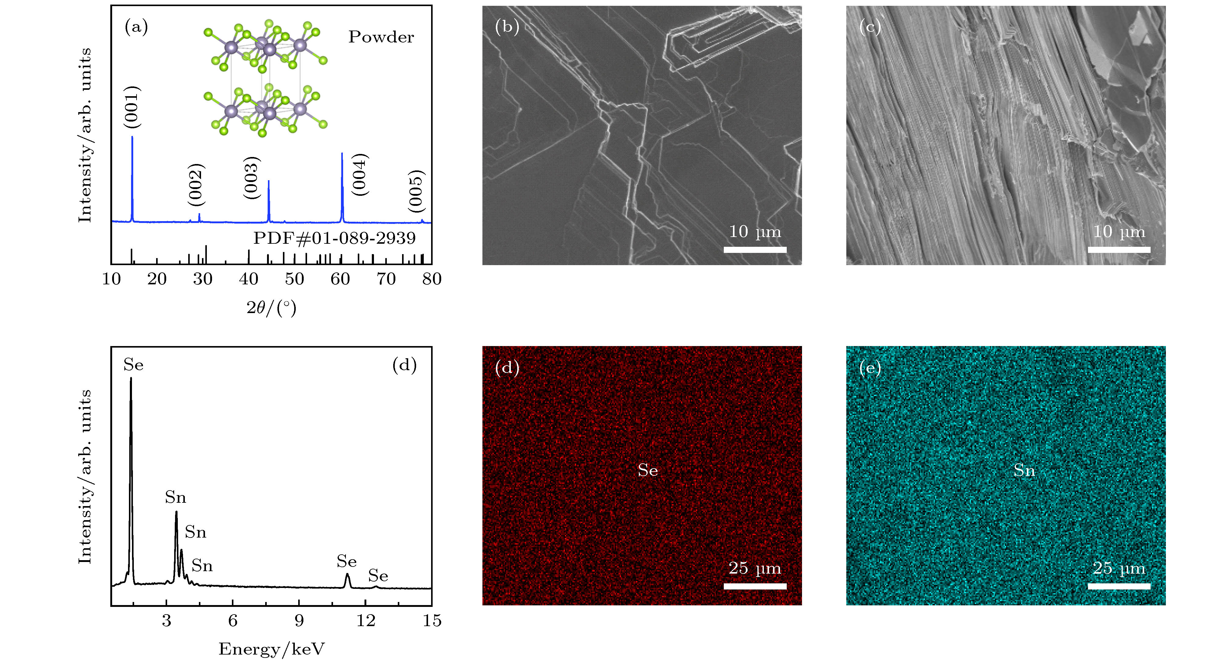
图 2 (a) SnSe2粉体XRD, 插图为样品的晶体结构; (b)和(c) 样品断面FESEM图; (d) EDS能谱图; (e) EDS面扫Se分布图; (f) EDS面扫Sn分布图
Figure 2. (a) XRD patterns of SnSe2, the inset is the crystal structure of the SnSe2; (b) and (c) FESEM images of the fresh fracture surface of SnSe2 after SPS synthesis; (d) EDS spectrum of SnSe2; (e) the Se elemental map and (f) the Sn elemental map.
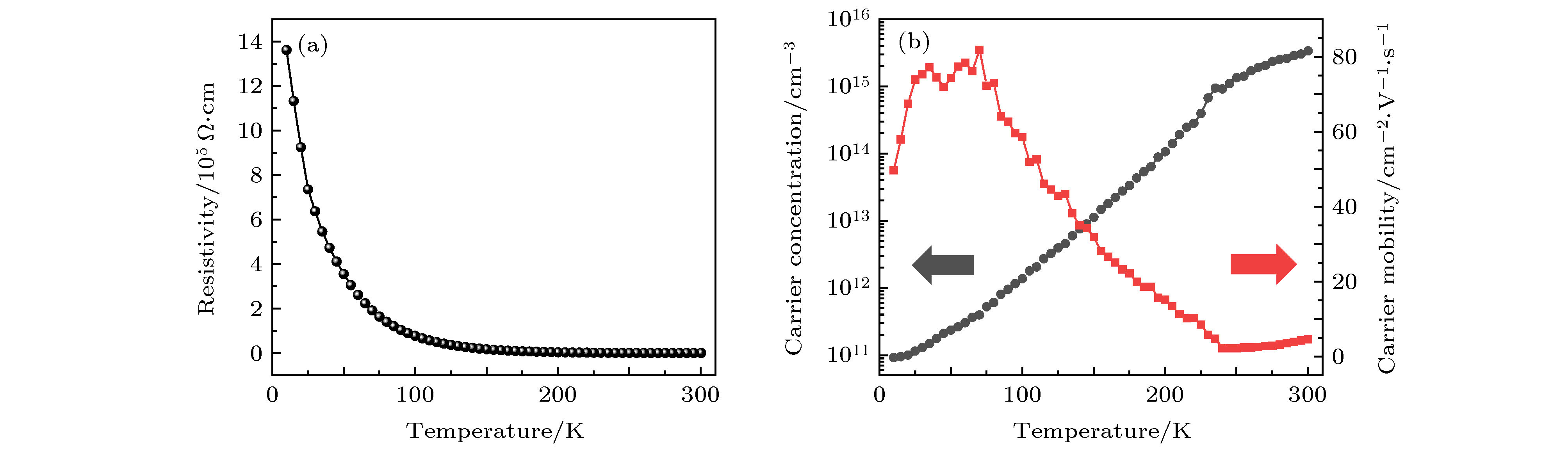
图 3 (a) 10−300 K下的ρ-T曲线; (b) 材料的载流子浓度与迁移率在10−300 K下的变化曲线
Figure 3. Temperature dependence (10−300 K) of the resistivity (a) and carrier concentration and mobility (b).

图 4 (a) 300 K下器件在–100 mA → 0 → 100 mA → 0 → –100 mA循环3次的V-I曲线, 插图为器件模型图; (b) 10 K下器件在–100 mA → 0 → 100 mA → 0 → –100 mA循环3次的V-I曲线
Figure 4. (a) V-I characteristic curves of SnSe2 with current sweep as –100 mA → 0 → 100 mA → 0 → –100 mA for 3 times at 300 K, the inset shows the schematic of the device; (b) V-I characteristic curves of SnSe2 with current sweep as –100 mA → 0 → 100 mA → 0 → –100 mA for 3 times at 10 K.

图 5 (a) 在环境温度285 K下(0 mA → 100 mA → 0 mA)的V-I循环图, 插图为器件未控温直接与空气进行热交换的红外测试示意图; (b)样品在(a)中A, B, C点时的温度分布; (c) SnSe2的DSC曲线
Figure 5. (a) V-I characteristic curves of SnSe2 in current sweep as 0 mA → 100 mA → 0 mA at ambient temperature 285 K, the inset shows the ultrared detection diagram of the device directly exchanging heat with air; (b) temperature distribution maps of the sample at temperature points A, B and C in (a); (c) the DSC curves of SnSe2.
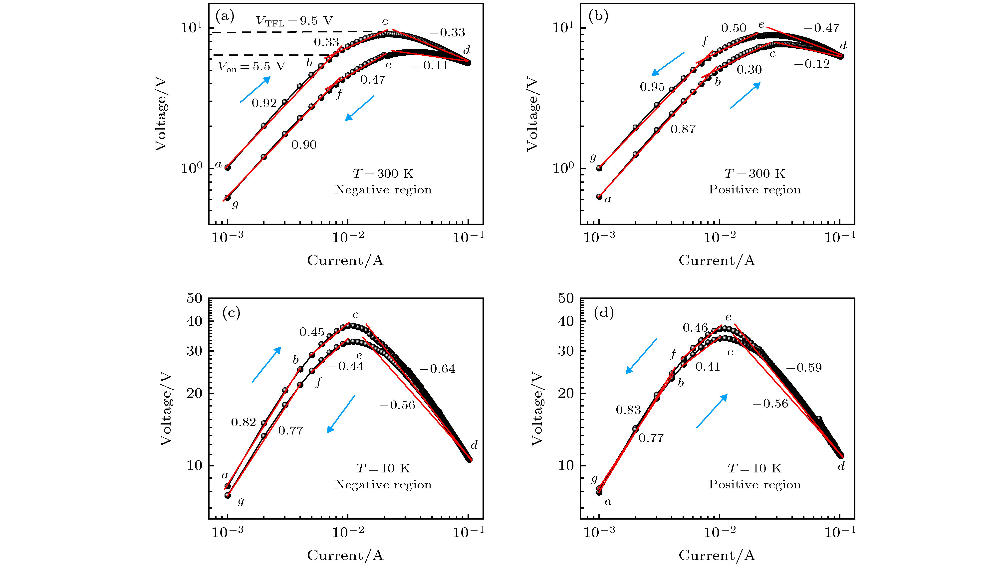
图 6 在300 K负向偏压下(a)和正向偏压下(b)的lgV-lgI图; 在10 K负向偏压下(c)和正向偏压下(d)的lgV-lgI图
Figure 6. lgV-lgI curves in negative bias region (a) and positive bias region (b) at 300 K, respectively; lgV-lgI curves in in negative bias region (c) and positive bias region (d) at 10 K, respectively.

图 7 不同磁场下的V-I曲线 (a) 300 K; (c) 200 K; (e) 100 K; (g) 10 K; 不同磁场下lgV-lgI曲线 (b) 300 K; (d) 200 K; (f) 100 K; (h) 10 K; 图(b)和图(d)中插图为曲线的局部放大图
Figure 7. V-I characteristic curves under different magnetic fields at 300 K (a), 200 K (c), 100 K (e) and 10 K (g), respectively; lgV-lgI characteristic curves under different magnetic fields at 300 K (b), 200 K (d), 100 K (f) and 10 K (h), respectively. The insets in (b) and (d) show the magnified parts of curves.
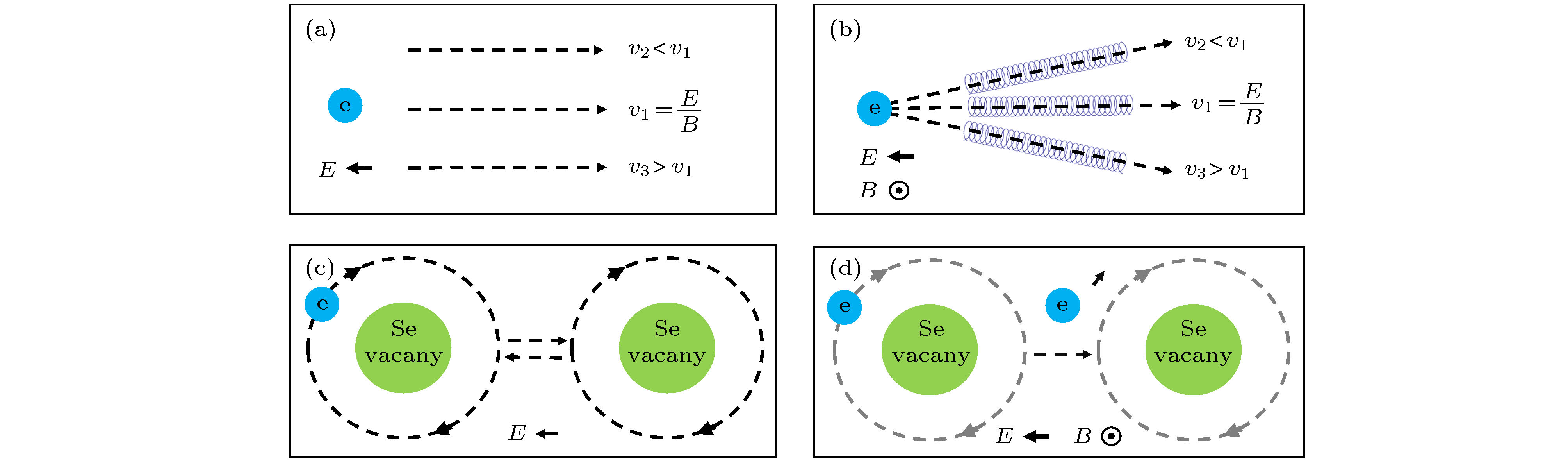
图 8 (a)晶格散射主导下的电子输运过程; (b) 磁场对晶格散射主导的电子运动过程影响; (c) 杂质散射主导的电子局域化行为; (d) 磁场对杂质散射时的电子局域化抑制行为
Figure 8. (a) Electron motion process dominated by lattice scattering; (b) influence of magnetic field on the electron motion process dominated by lattice scattering; (c) electron localization process dominated by impurity scattering; (d) influence of magnetic field on the electron localization process dominated by impurity scattering.
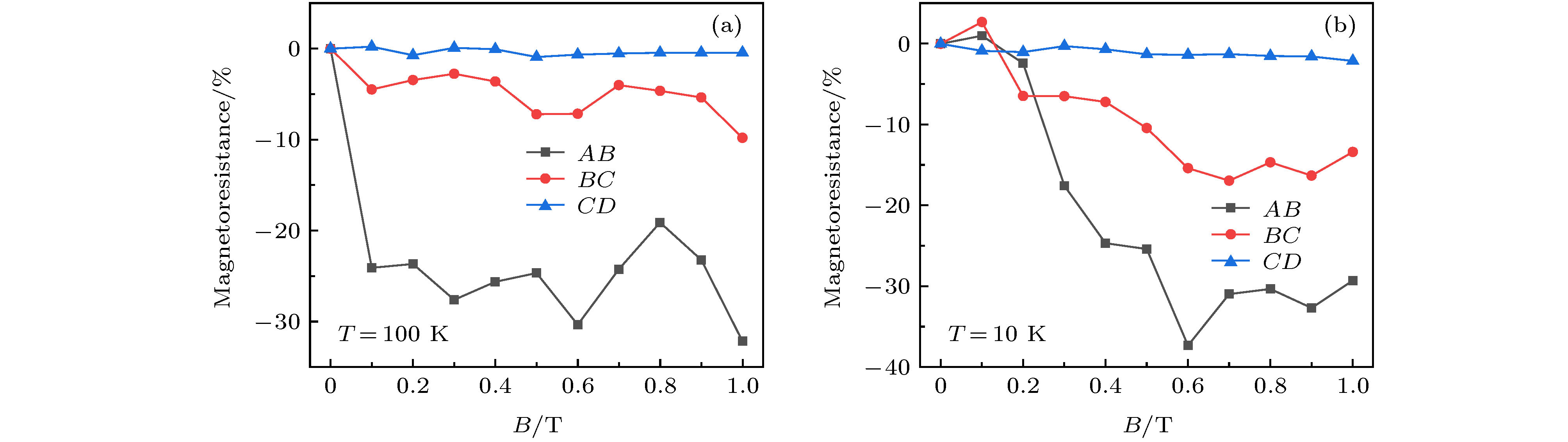
图 9 (a) 100 K不同区域下MR-B曲线; (b) 10 K不同区域下MR-B曲线
Figure 9. (a) MR-B curves in different regions at 100 K; (b) MR-B curves in different regions at 10 K.
-
[1] Chua L 1971 IEEE Trans. Circuit Theory 18 507
Google Scholar
[2] Sawa A 2008 Mater. Today 11 28
[3] Waser R, Dittmann R, Staikov G, Szot K 2009 Adv. Mater. 21 2632
Google Scholar
[4] Segui Y, Ai B, Carchano H 1976 J. Appl. Phys. 47 140
Google Scholar
[5] Scott J C, Bozano L D 2007 Adv. Mater. 19 1452
Google Scholar
[6] 缪向水, 李祎, 孙华军, 薛堪豪 2018 忆阻器导论 (北京: 科学出版社) 第14−20页
Miu X S, Li W, Sun H J, Xue K H 2018 Introduction to memristor (Beijing: Science Press) pp14−20 (in Chinese)
[7] 刘东青, 程海峰, 朱玄, 王楠楠, 张朝阳 2014 物理学报 63 187301
Google Scholar
Liu D Q, Cheng H F, Zhu X, Wang N N, Zhang C Y 2014 Acta Phys. Sin. 63 187301
Google Scholar
[8] Windeln J, Bram C, Eckes H L, Hammel D, Huth J, Marien J, Röhl H, Schug C, Wahl M, Wienss A 2001 Appl. Surf. Sci. 179 167
Google Scholar
[9] 韩秀峰 2014 自旋电子学导论 (北京: 科学出版社) 第13−20页
Han X F 2014 Introduction to Spintronics (Beijing: Science Press) pp13−20 (in Chinese)
[10] Prezioso M, Riminucci A, Graziosi P, Bergenti I, Rakshit R, Cecchini R, Vianelli A, Borgatti F, Haag N, Willis M, Drew A J, Gillin W P, Dediu V A 2013 Adv. Mater. 25 534
Google Scholar
[11] Tang Y, Li D C, Chen Z, Deng S P, Sun L Q, Liu W T, Shen L X, Deng S K 2018 Chin. Phys. B 27 118105
Google Scholar
[12] Liu C Y, Miao L, Wang X Y, Wu S H, Zheng Y Y, Deng Z Y, Chen Y L, Wang G W, Zhou X Y 2018 Chin. Phys. B 27 047211
Google Scholar
[13] Borges Z V, Poffo C M, de Lima J C, de Souza S M, Triches D M, Nogueira T P O, Manzato L, de Biasi R S 2016 Mater. Chem. Phys. 169 47
Google Scholar
[14] Chung K M, Wamwangi D, Woda M, Wuttig M, Bensch W 2008 J. Appl. Phys. 103 083523
Google Scholar
[15] Micoulaut M, Welnic W, Wuttig M 2008 Phys. Rev. B 78 224209
Google Scholar
[16] Wang R Y, Caldwell M A, Jeyasingh R G D, Aloni S, Shelby R M, Wong H S P, Milliron D J 2011 J. Appl. Phys. 109 113506
Google Scholar
[17] Lee S, Lee Y T, Park S G, Lee K H, Kim S W, Hwang D K, Lee K 2018 Adv. Electron. Mater. 4 1700563
Google Scholar
[18] Xu P P, Fu T Z, Xin J Z, Liu Y T, Ying P J, Zhao X B, Pan H G, Zhu T J 2017 Sci. Bull. 62 1663
Google Scholar
[19] Zhou X, Gan L, Tian W M, Zhang Q, Jin S Y, Li H Q, Bando Y, Golberg D, Zhai T Y 2015 Adv. Mater. 27 8035
Google Scholar
[20] Fernandes P A, Sousa M G, Salome P M P, Leitao J P, da Cunha A F 2013 Crystengcomm 15 10278
Google Scholar
[21] Saha S, Banik A, Biswas K 2016 Chem. Eur. J. 22 15634
Google Scholar
[22] Shu Y J, Su X L, Xie H Y, Zheng G, Liu W, Yan Y G, Luo T T, Yang X, Yang D W, Uher C, Tang X F 2018 ACS Appl. Mater. Interfaces 10 15793
Google Scholar
[23] Jameson J R, Gilbert N, Koushan F, Saenz J, Wang J, Hollmer S, Kozicki M N 2011 Appl. Phys. Lett. 99 063506
Google Scholar
[24] van den Hurk J, Havel V, Linn E, Waser R, Valov I 2013 Sci. Rep. 3 2856
Google Scholar
[25] van den Hurk J, Dippel A C, Cho D Y, Straquadine J, Breuer U, Walter P, Waser R, Valov I 2014 Phys. Chem. Chem. Phys. 16 18217
Google Scholar
[26] Hasegawa T, Terabe K, Nakayama T, Aono M 2005 Nature 433 47
Google Scholar
[27] Ohno T, Hasegawa T, Nayak A, Tsuruoka T, Gimzewski J K, Aono M 2011 Appl. Phys. Lett. 99 203108
Google Scholar
[28] Zhang J J, Sun H J, Li Y, Wang Q, Xu X H, Miao X S 2013 Appl. Phys. Lett. 102 183513
Google Scholar
[29] Wuttig M, Yamada N 2007 Nat. Mater. 6 824
Google Scholar
[30] Han N, Kim S I, Yang J D, Lee K, Sohn H, So H M, Ahn C W, Yoo K H 2011 Adv. Mater. 23 1871
Google Scholar
[31] Li Y, Zhong Y P, Zhang J J, Xu X H, Wang Q, Xu L, Sun H J, Miao X S 2013 Appl. Phys. Lett. 103 043501
Google Scholar
[32] Wiedemeier H, Pultz G, Gaur U, Wunderlich B 1981 Thermochim. Acta 43 297
Google Scholar
[33] Lagnier R, Ayache C, Harbec J Y, Jandl S, Jay-Gerin J P 1983 Solid State Commun. 48 65
[34] Shang D S, Wang Q, Chen L D, Dong R, Li X M, Zhang W Q 2006 Phys. Rev. B 73 245427
Google Scholar
[35] Du Y M, Pan H, Wang S J, Wu T, Feng Y P, Pan J S, Wee A T S 2012 Acs Nano 6 2517
Google Scholar
[36] Chen X G, Ma X B, Yang Y B, Chen L P, Xiong G C, Lian G J, Yang Y C, Yang J B 2011 Appl. Phys. Lett. 98 122102
Google Scholar
[37] Mark P, Helfrich W 1962 J. Appl. Phys. 33 205
Google Scholar
[38] Montero J M, Bisquert J 2011 J. Appl. Phys. 110 327
[39] Lampert M A 1956 Phys. Rev. 103 1648
Google Scholar
[40] Kytin V, Dittrich T, Koch F, Lebedev E 2001 Appl. Phys. Lett. 79 108
Google Scholar
[41] Zhang W, Thiess A, Zalden P, Zeller R, Dederichs P H, Raty J Y, Wuttig M, Bluegel S, Mazzarello R 2012 Nat. Mater. 11 952
Google Scholar

 DownLoad:
Catalog
Metrics
- Abstract views: 13174
- PDF Downloads: 174
- Cited By: 0
