-
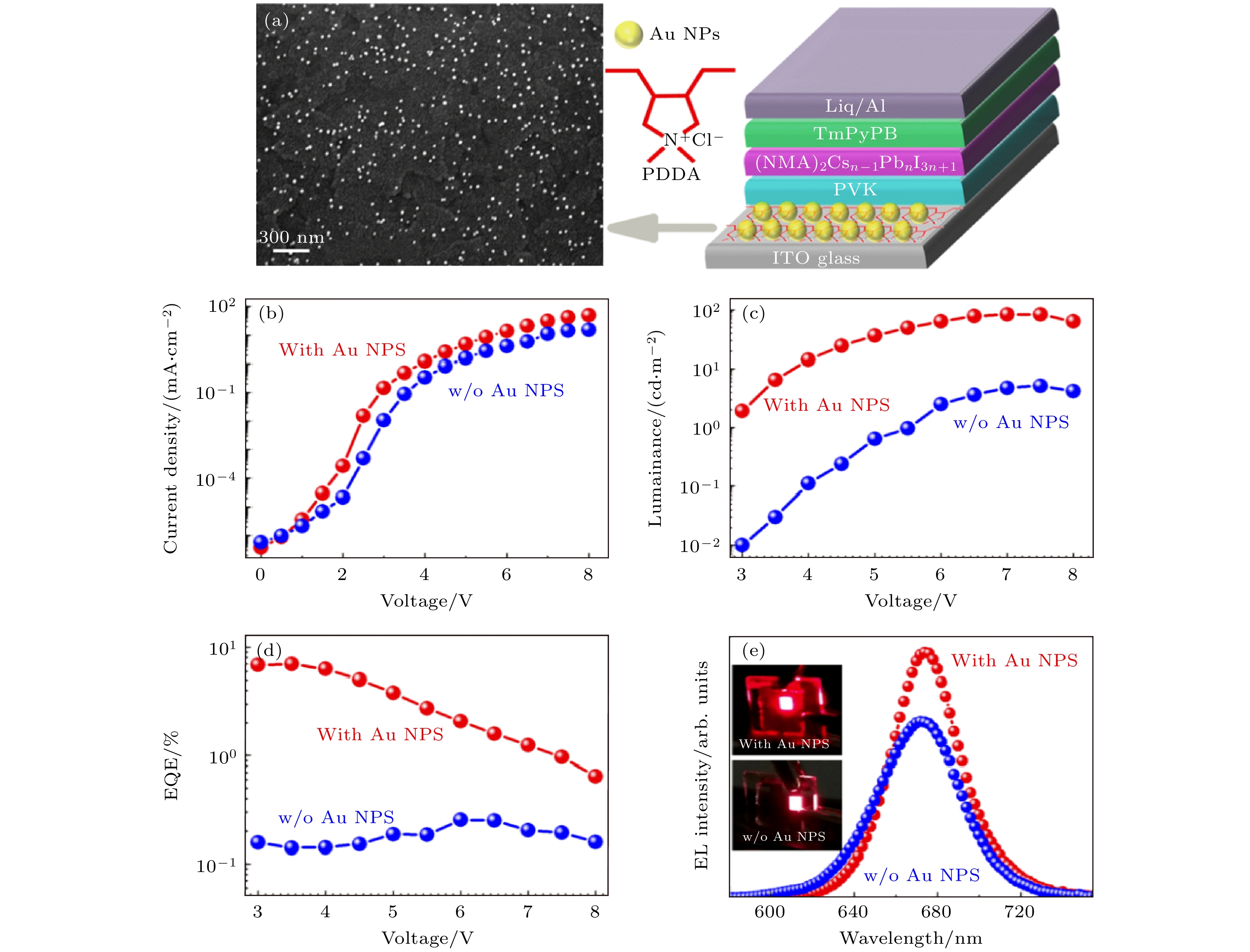
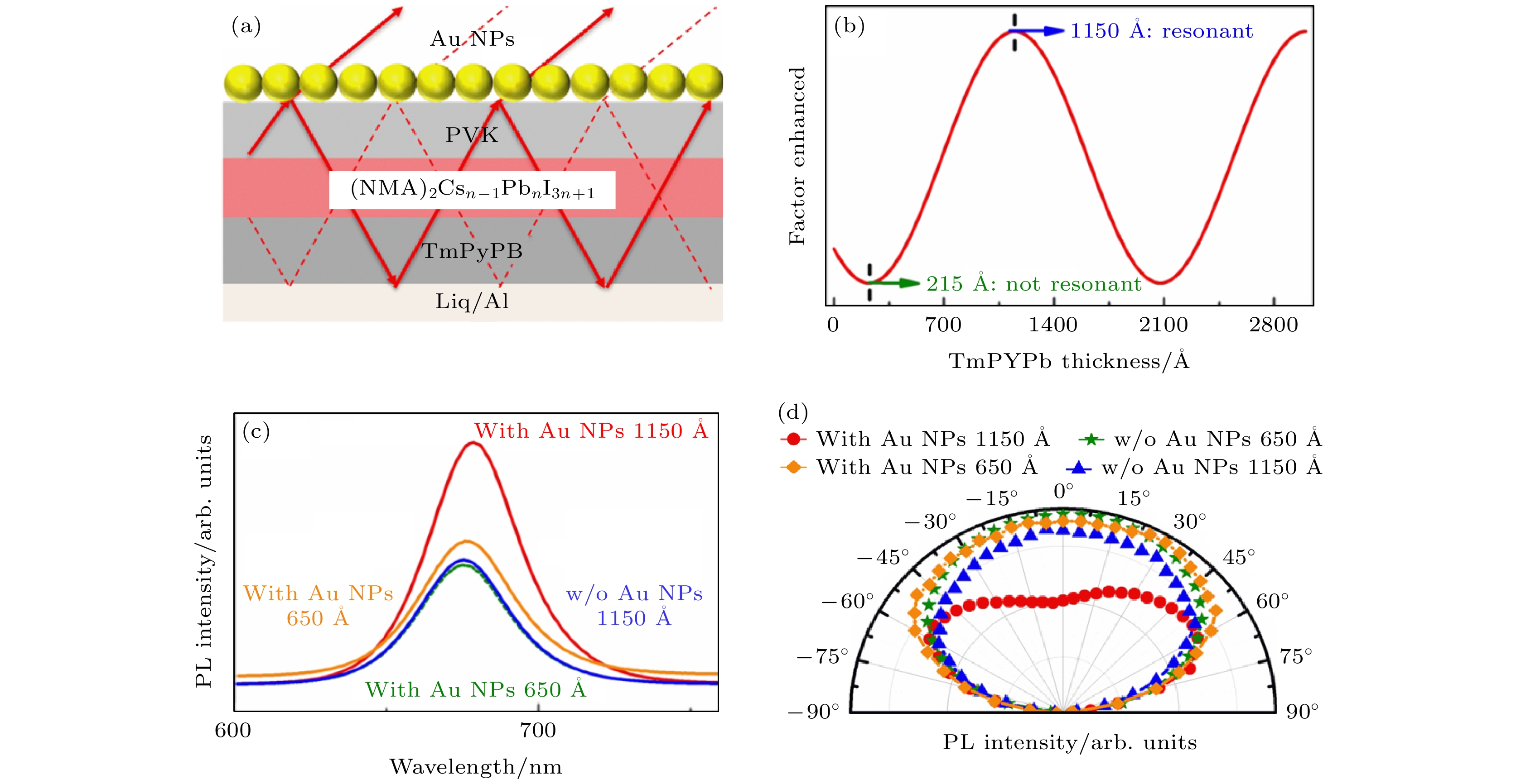
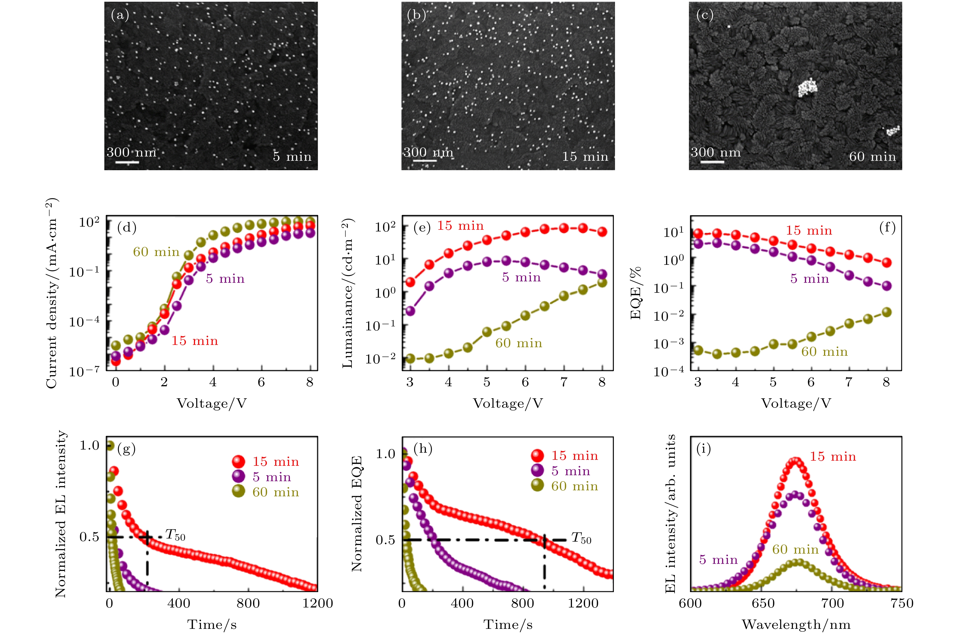
Gold nanoparticles (Au NPs) play an important role in improving the external quantum efficiency of perovskite light emitting diodes (PeLED). To avoid direct contact between the Au NPs and the light emitting layer, the Au NPs@SiO2 structure and blending the Au NPs into the hole transport layer (HTL) or electron transport layer (ETL) have been proposed previously. However, the Au NPs@SiO2 is difficult to obtain and affects the charge transport. When the Au NPs is blended in poly(3,4-ethylene dioxythiophene):poly(styrene sulfonate) (PEDOT: PSS), the density of Au NPs is not easily controlled and the PEDOT:PSS is not an ideal HTL for PeLED. Therefore, the electrostatic adsorption is used in this work to uniformly disperse the ~20 nm-size Au NPs on the top of the ITO anode, and the Poly(9-vinylcarbazole) (PVK) is spin-coated as the HTL to achieve the high performance red PeLED based on the (NMA)2Csn–1PbnI3n+1. After the Au NPs modification, the maximum luminous brightness rises from ~5.2 to ~83.2 cd/m2. Meanwhile, the maximum external quantum efficiency rises from ~0.255% to ~6.98%. Mechanism studies show that microcavity can be formed between the Au NPs-modified ITO anode and the Al cathode, and the transmitted light and the reflected light interfere with each other to improve the output couple efficiency of the PeLED. The photoluminescence (PL) spectrum and angle dependent PL intensity of the Au NPs-modified PeLED prove that the fluorescence enhancement of the (NMA)2Csn–1PbnI3n+1 perovskite is attributed mainly to the microcavity effect. Furthermore, the effects of Au NPs density on the performance of the PeLED are investigated, which reveals that the device with ~15 min adsorption is optimal. Finally, we rule out the contributions of Au NPs to the morphology, crystallization, electrical properties and localized surface plasmon resonance (LSPR) effects of (NMA)2Csn–1PbnI3n+1 perovskite films. In this work, the Au NPs are successfully applied to red PeLED for the first time, providing a feasible way of developing the low-cost and high-efficiency PeLED.
-
Keywords:
- gold nanoparticals /
- electrostatic adsorption /
- micocavity effect /
- perovskite light emitting diodes
[1] Qian J Y, Xu B, Tian W J 2016 Org. Electron. 37 61
 Google Scholar
[2] Yuan M J, Quan L N, Comin R, Walters G, Sabatini R, Voznyy O, Hoogland S, Zhao Y B, Beauregard E M, Kanjanaboos P, Lu Z H, Kim D H, Sargent E H 2016 Nat. Nanotechnol. 11 872
 Google Scholar
[3] Lozano G 2018 Phys. Chem. Lett. 9 3987
 Google Scholar
[4] Song Z, Zhao J, Liu Q L 2019 Inorg. Chem. Front. 6 2969
 Google Scholar
[5] Wu H, Yang Y, Zhou D, Li K, Yu J, Han J, Li Z, Long Z, Ma J, Qiu J 2018 Nanoscale 10 3429
 Google Scholar
[6] Tan Z K, Moghaddam R S, Lai M L, Docampo P, Higler R, Deschler F, Price M, Sadhanala A, Pazos L M, Credgington, Hanusch F, Bein, Snaith H J, Friend R 2018 Nat. Nanotechnol. 9 687
 Google Scholar
[7] Fang Z B, Chen W J, Shi Y L, Zhao J, Chu S, Zhang J, Xiao Z G 2020 Adv. Funct. Mater. 30 1909754
 Google Scholar
[8] Vashishth P, Halper J E 2017 Chem. Mater. 29 5965
 Google Scholar
[9] Kim D H, Kim Y C, An H J, Myoung J M 2020 J. Alloys Compd. 845 156272
 Google Scholar
[10] Jiang Y, Qin C, Cui M, He T, Liu K, Huang Y, Luo M, Zhang L, Xu H, Li S 2019 Nat. Commun. 10 1868
 Google Scholar
[11] Fu X, Mehta Y, Chen Y, Lei L, So F 2021 Adv. Mater. 33 2006801
 Google Scholar
[12] Zhang Y, Sun H, Zhang S, Li S, Wang X, Zhang X, Liu T, Guo Z 2019 Opt. Mater. 89 563
 Google Scholar
[13] Chen P, Xiong Z, Wu X, Shao M, Gao C 2017 J. Phys. Chem. Lett. 8 3961
 Google Scholar
[14] Lin H H, Chen I C 2015 J. Phys. Chem. C. 119 26663
 Google Scholar
[15] Tiwari A, Satpute N S, Mehare C M, Dhoble S J 2020 J. Alloys Compd. 850 156827
 Google Scholar
[16] Sum T C, Righetto M, Lim S S 2020 J. Chem. Phys. 152 130901
 Google Scholar
[17] Guo Y W, Jia Y H, Li N, Chen M Y, Hu S J, Liu C, Zhao N 2020 Adv. Funct. Mater. 30 1910464
 Google Scholar
[18] Shen Y, Li M N, Li Y, Xie F M, Tang J X 2020 ACS Nano. 14 6107
 Google Scholar
[19] Wang S P, Chang C K, Yang S H, Chang C Y, Chao Y C 2018 Mater. Res. Express 5 015037
 Google Scholar
[20] Dodabalapur A, Rothberg L J, Jordan R H, Miller T M, Slusher R E, Phillips J M 1996 J. Appl. Phys. 80 6954
 Google Scholar
[21] Jain P K, Lee K S, El-Sayed I H, El-Sayed M A 2006 J. Phys. Chem. B 110 7238
[22] Daniel M C, Astruc D 2004 Chem. Rev. 104 293
 Google Scholar
[23] Sun G, Khurgin J B, Soref R A 2009 Appl. Phys. Lett. 94 101103
 Google Scholar
[24] Peng J, Xu X, Tian Y, Wang J, Tang F, Li L 2014 Appl. Phys. Lett. 105 173301
 Google Scholar
[25] Wu X Y, Liu L L, Yu T C, Yu L, Xie Z Q, Mo Y Q, Xu S P, Ma Y G 2013 J. Mater. Chem. C 1 7020
 Google Scholar
[26] Meng Y, Wu X Y, Xiong Z Y, Lin C Y, Xiong Z H 2018 Nanotechnology 29 175203
 Google Scholar
[27] Xu T, Li W, Wu X, Ahmadi M, Xu L 2020 J. Mater. Chem. C 8 6615
 Google Scholar
[28] Meng Y, Ahmadi M, Wu X Y, Xu T F, Xu L, Xiong Z H, Chen P 2018 Org. Electron. 64 47
 Google Scholar
[29] Li T, Xiang T, Wang M S, Zhang W, Shi J S, Shao M, Xu T F, Ahmadi M, Wu X Y, Gao Z, Xu L, Chen P 2021 Laser Photonics Rev. doi: 10.1002/lpor.202000495
[30] Jbara A S, Munir J, Ul Haq B, Saeed M A 2020 Appl. Opt. 59 3751
 Google Scholar
[31] Lee J, Song J, Park J, Yoo S 2021 Adv. Opt. Mater. doi: 10.1002/adom.202002182
[32] Miao Y F, Cheng L, Zou W, Gu L H, Zhang J, Guo Q, Peng Q M, Xu M M, He Y R, Zhang S T, Cao Y, Li R Z, Wang N N, Huang W, Wang J P 2020 Light-Sci. Appl. 9 89
 Google Scholar
[33] Lu M, Zhang Y, Wang S X, Guo J, Yu W W, Rogach A L 2019 Adv. Funct. Mater. 2019 29 1902008
[34] Yuichiro, Kawamura, Hiroyuki, Sasabe, Chihaya 2005 Jpn. J. Appl. Phys. 44 1160
 Google Scholar
[35] Zhang J, Zhang L, Cai P, Xue X, Wang M, Zhang J, Tu G 2019 Nano Energy 62 434
 Google Scholar
[36] Kumar M, Pawar V, Jha P A, Gupta S K, Sinha A S K, Jha P K, Singh P 2019 J. Mater. Sci. -Mater. Electron. 30 6071
 Google Scholar
[37] Eperon G E, Paternò G M, Sutton R J, Zampetti A, Haghighirad A A, Cacialli F, Snaith H J 2015 J. Mater. Chem. A 3 19688
 Google Scholar
[38] Bulovic V, Khalfin V B, Gu G, Burrows P E 1998 Phys. Rev. B 58 3730
 Google Scholar
[39] He Z F, Liu Y, Yang Z L, Li J, Cui J Y, Chen D, Fang Z S, He H P, Ye Z Z, Zhu H M, Wang N N, Wang J P, Jin Y Z 2019 ACS Photonics 2019 6 587
-
图 1 (a) 15 min静电吸附的Au NPs修饰的ITO表面的SEM图像和Au NPs修饰的PeLED结构示意图, 插图展示了Au NPs和PDDA分子式; 有、无Au NPs修饰的PeLED的(b)电流密度-电压 (J-V) 曲线, (c)亮度-电压曲线 (L-V) , (d)外量子效率 ( EQE-V) 曲线以及 (e) 约6 V下的EL谱
Figure 1. (a) SEM image of the Au NPs modified ITO with 15 min electrostatic adsorption and schematic diagram of the device structure of Au NPs modified PeLED, the insets show the Au NPs and the molecular structure of PDDA; (b) the J-V curve, (c) the L-V curve, (d) EQE-V curve of PeLEDs with and without Au NPs modification, (e) EL spectrum of PeLEDs with and without Au NPs modification working at about 6 V.
图 2 有、无Au NPs修饰的(NMA)2Csn–1PbnI3n+1钙钛矿薄膜 (a), (b) SEM图; (c) XRD图; (d), (e) UPS图; (f)单空穴器件的J-V曲线; (g) Au NPs溶液的吸收谱和有、无Au NPs修饰的(NMA)2Csn–1PbnI3n+1钙钛矿层的PL发射谱; (h)有、无Au NPs修饰的(NMA)2Csn–1PbnI3n+1薄膜PL lifetime曲线
Figure 2. SEM images of (NMA)2Csn–1PbnI3n+1 film (a) with and (b)without Au NPs; (c) XRD patterns of (NMA)2Csn–1PbnI3n+1 film with and without Au NPs; (d), (e) UPS characterizations of (NMA)2Csn–1PbnI3n+1 film with and without Au NPs; (f) J-V curves of hole-only devices with and without Au NPs; (g) the absorption spectra of the Au NPs solution and the PL spectrums of the (NMA)2Csn–1PbnI3n+1 film with and without Au NPs; (h) PL lifetime decay curve of the (NMA)2Csn–1PbnI3n+1 film with and without the Au NPs.
图 3 (a) 谐振腔结构示意图; (b) PL发射强度随TmPYPb厚度的变化曲线; 有、无Au NPs修饰的PeLED器件在不同TmPYPb厚度 (650, 1150 Å) 时的(c) PL发射谱和(d) PL强度随角度变化曲线
Figure 3. (a) Schematic diagram of the micocavity structure; (b) the simulated evolution of PL intensity with TmPYPb thickness; (c) the PL spectrums and (d) the angle dependent of PL intensities of the PeLEDs with and without Au NPs at different TmPYPb thicknesses of about 650 and 1150 Å.
图 4 (a)—(c) 依次为5, 15和60 min吸附时间的Au NPs在ITO表面的SEM图像; 5, 15和60 min PeLED的(d) J-V特性曲线, (e) L-V特性曲线和(f) EQE-V特性曲线; 5, 15和60 min PeLED的(g)亮度随时间变化和(h) EQE随时间变化曲线; (i) 5, 15和60 min PeLED在6 V下的EL谱
Figure 4. (a)−(c) SEM images of Au NPs modified ITO substrates with 5, 15, and 60 min electrostatic adsorption, respectively; (d)−(f) J-V , L-V and EQE-V curves for 5, 15, and 60 min electrostatic adsorption, respectively; (g), (h) time evolutions of Lmax and EQEmax of PeLEDs with 5, 15, and 60 min electrostatic adsorption, respectively; (i) EL spectra of PeLEDs with 5, 15, and 60 min electrostatic adsorption working at about 6 V.
表 1 有、无Au NPs修饰的(NMA)2Csn–1PbnI3n+1钙钛矿薄膜的荧光寿命拟合参数
Table 1. Fitting parameters for PL lifetimes of the (NMA)2Csn–1PbnI3n+1 films with and without Au NPs.
Au NPs A1/% A2/% A3/% τ1/ns τ2/ns τ3/ns χ2 有 35.02 56.34 8.64 2.78 8.97 41.57 1.12 无 35.31 57.68 7.00 2.43 8.33 43.92 1.05 表 2 各层光学折射率及其厚度总结
Table 2. Summaries of optical refractive index and thickness of each layer.
PVK (NMA)2
Csn–1PbnI3n+1TmPYPb Liq 折射率 n 1.5624 2.46 1.75 1.5 厚度 d/nm 35 35 115 2.5 -
[1] Qian J Y, Xu B, Tian W J 2016 Org. Electron. 37 61
 Google Scholar
[2] Yuan M J, Quan L N, Comin R, Walters G, Sabatini R, Voznyy O, Hoogland S, Zhao Y B, Beauregard E M, Kanjanaboos P, Lu Z H, Kim D H, Sargent E H 2016 Nat. Nanotechnol. 11 872
 Google Scholar
[3] Lozano G 2018 Phys. Chem. Lett. 9 3987
 Google Scholar
[4] Song Z, Zhao J, Liu Q L 2019 Inorg. Chem. Front. 6 2969
 Google Scholar
[5] Wu H, Yang Y, Zhou D, Li K, Yu J, Han J, Li Z, Long Z, Ma J, Qiu J 2018 Nanoscale 10 3429
 Google Scholar
[6] Tan Z K, Moghaddam R S, Lai M L, Docampo P, Higler R, Deschler F, Price M, Sadhanala A, Pazos L M, Credgington, Hanusch F, Bein, Snaith H J, Friend R 2018 Nat. Nanotechnol. 9 687
 Google Scholar
[7] Fang Z B, Chen W J, Shi Y L, Zhao J, Chu S, Zhang J, Xiao Z G 2020 Adv. Funct. Mater. 30 1909754
 Google Scholar
[8] Vashishth P, Halper J E 2017 Chem. Mater. 29 5965
 Google Scholar
[9] Kim D H, Kim Y C, An H J, Myoung J M 2020 J. Alloys Compd. 845 156272
 Google Scholar
[10] Jiang Y, Qin C, Cui M, He T, Liu K, Huang Y, Luo M, Zhang L, Xu H, Li S 2019 Nat. Commun. 10 1868
 Google Scholar
[11] Fu X, Mehta Y, Chen Y, Lei L, So F 2021 Adv. Mater. 33 2006801
 Google Scholar
[12] Zhang Y, Sun H, Zhang S, Li S, Wang X, Zhang X, Liu T, Guo Z 2019 Opt. Mater. 89 563
 Google Scholar
[13] Chen P, Xiong Z, Wu X, Shao M, Gao C 2017 J. Phys. Chem. Lett. 8 3961
 Google Scholar
[14] Lin H H, Chen I C 2015 J. Phys. Chem. C. 119 26663
 Google Scholar
[15] Tiwari A, Satpute N S, Mehare C M, Dhoble S J 2020 J. Alloys Compd. 850 156827
 Google Scholar
[16] Sum T C, Righetto M, Lim S S 2020 J. Chem. Phys. 152 130901
 Google Scholar
[17] Guo Y W, Jia Y H, Li N, Chen M Y, Hu S J, Liu C, Zhao N 2020 Adv. Funct. Mater. 30 1910464
 Google Scholar
[18] Shen Y, Li M N, Li Y, Xie F M, Tang J X 2020 ACS Nano. 14 6107
 Google Scholar
[19] Wang S P, Chang C K, Yang S H, Chang C Y, Chao Y C 2018 Mater. Res. Express 5 015037
 Google Scholar
[20] Dodabalapur A, Rothberg L J, Jordan R H, Miller T M, Slusher R E, Phillips J M 1996 J. Appl. Phys. 80 6954
 Google Scholar
[21] Jain P K, Lee K S, El-Sayed I H, El-Sayed M A 2006 J. Phys. Chem. B 110 7238
[22] Daniel M C, Astruc D 2004 Chem. Rev. 104 293
 Google Scholar
[23] Sun G, Khurgin J B, Soref R A 2009 Appl. Phys. Lett. 94 101103
 Google Scholar
[24] Peng J, Xu X, Tian Y, Wang J, Tang F, Li L 2014 Appl. Phys. Lett. 105 173301
 Google Scholar
[25] Wu X Y, Liu L L, Yu T C, Yu L, Xie Z Q, Mo Y Q, Xu S P, Ma Y G 2013 J. Mater. Chem. C 1 7020
 Google Scholar
[26] Meng Y, Wu X Y, Xiong Z Y, Lin C Y, Xiong Z H 2018 Nanotechnology 29 175203
 Google Scholar
[27] Xu T, Li W, Wu X, Ahmadi M, Xu L 2020 J. Mater. Chem. C 8 6615
 Google Scholar
[28] Meng Y, Ahmadi M, Wu X Y, Xu T F, Xu L, Xiong Z H, Chen P 2018 Org. Electron. 64 47
 Google Scholar
[29] Li T, Xiang T, Wang M S, Zhang W, Shi J S, Shao M, Xu T F, Ahmadi M, Wu X Y, Gao Z, Xu L, Chen P 2021 Laser Photonics Rev. doi: 10.1002/lpor.202000495
[30] Jbara A S, Munir J, Ul Haq B, Saeed M A 2020 Appl. Opt. 59 3751
 Google Scholar
[31] Lee J, Song J, Park J, Yoo S 2021 Adv. Opt. Mater. doi: 10.1002/adom.202002182
[32] Miao Y F, Cheng L, Zou W, Gu L H, Zhang J, Guo Q, Peng Q M, Xu M M, He Y R, Zhang S T, Cao Y, Li R Z, Wang N N, Huang W, Wang J P 2020 Light-Sci. Appl. 9 89
 Google Scholar
[33] Lu M, Zhang Y, Wang S X, Guo J, Yu W W, Rogach A L 2019 Adv. Funct. Mater. 2019 29 1902008
[34] Yuichiro, Kawamura, Hiroyuki, Sasabe, Chihaya 2005 Jpn. J. Appl. Phys. 44 1160
 Google Scholar
[35] Zhang J, Zhang L, Cai P, Xue X, Wang M, Zhang J, Tu G 2019 Nano Energy 62 434
 Google Scholar
[36] Kumar M, Pawar V, Jha P A, Gupta S K, Sinha A S K, Jha P K, Singh P 2019 J. Mater. Sci. -Mater. Electron. 30 6071
 Google Scholar
[37] Eperon G E, Paternò G M, Sutton R J, Zampetti A, Haghighirad A A, Cacialli F, Snaith H J 2015 J. Mater. Chem. A 3 19688
 Google Scholar
[38] Bulovic V, Khalfin V B, Gu G, Burrows P E 1998 Phys. Rev. B 58 3730
 Google Scholar
[39] He Z F, Liu Y, Yang Z L, Li J, Cui J Y, Chen D, Fang Z S, He H P, Ye Z Z, Zhu H M, Wang N N, Wang J P, Jin Y Z 2019 ACS Photonics 2019 6 587
-
 20-20210500-2附加材料.pdf

Catalog
Metrics
- Abstract views: 8374
- PDF Downloads: 105
- Cited By: 0


 DownLoad:


