-
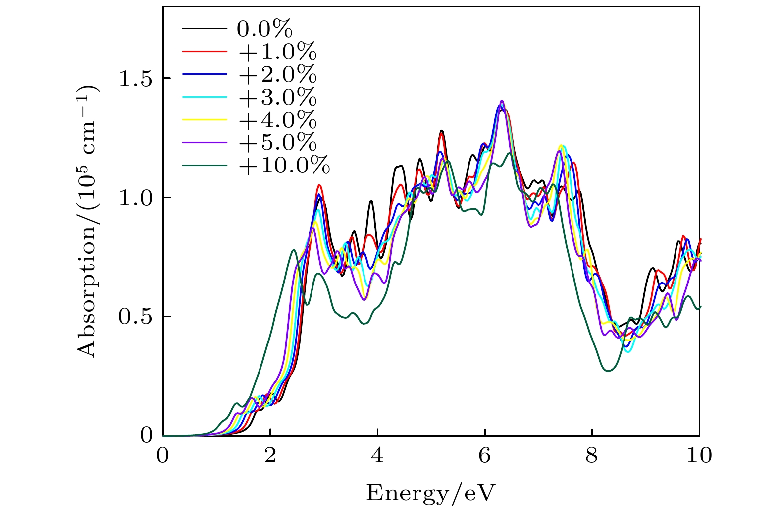
Monolayer molybdenum disulfide is an ideal material for making various micro/nano components and flexible electronic devices. However, the strain of material caused by the environment is a key problem that cannot be avoided in practical applications, and the electronic structure of material will also change with the strain. In this paper, the effect of tensile strain on the photoelectric properties of monolayer MoS2 is studied based on first principles and tensile tests after wet transfer. The results are obtained as follows. 1) Intrinsic monolayer MoS2 is a direct bandgap semiconductor with a band gap of 1.68 eV, the highest peak of the absorption coefficient curve is nearly 10.92 eV, and a maximum absorption coefficient is 1.66 × 105 cm–1. 2) A small tensile strain (1%) will result in the transition from direct to indirect gap for monolayer MoS2. With the increase of strain, the feature of the indirect gap can be preserved but the gap decreases linearly. The gap will decrease to 0 eV when the tensile strain is 10%, and the absorption coefficient curve is red-shifted as a whole with strain. 3) The in-plane mode peak and the out-of-plane mode A1g peak in Raman spectra are re-dshifted with stretching by tensile test of wet-transferred monolayer MoS2, and the difference in peak frequency between the two peaks is maintained at about 18.6 cm–1. The strong emission peak of an exciton of monolayer MoS2 is observed at 1.83 eV of the photoluminescenc spectrum. With the increase of tensile strain, the relative strength of the peak decreases and is linearly re-dshifted, which means that the band gap decreases linearly. It is consistent with the theoretical calculation result.
-
Keywords:
- molybdenum disulfide /
- tensile strain /
- energy bands /
- first principles
[1] Lin J, Zhong J, Zhong S, Li H, Zhang H, Chen W 2013 Appl. Phys. Lett. 103 063109
 Google Scholar
[2] Yin Z, Zhang X, Cai Y, Chen J, Wong J I, Tay Y Y 2014 Angew. Chem. Int. Ed. 53 12560
 Google Scholar
[3] Que H F, Jiang H N, Wang X G, Zhai P B, Meng L J, Zhang P, Gong Y J 2021 Acta Phys-Chim Sin. 37 2010051
 Google Scholar
[4] Kumar S, Sharma A, Tomar M, Gupta V 2021 Mater. Sci. Eng. B 266 11
 Google Scholar
[5] Tetsuka H, Nagoya A, Tamura S I 2016 Nanoscale 8 19677
 Google Scholar
[6] Singh E, Kim K S, Yeom G Y, Nalwa H S 2017 RSC Advan. 7 28234
 Google Scholar
[7] Pak S, Jang A R, Lee J, Hong J, Giraud P, Lee S 2019 Nanoscale 11 4726
 Google Scholar
[8] Liu Y, Weiss N O, Duan X D, Cheng H C, Huang Y, Duan X F 2016 Nat. Rev. Mater. 1 17
 Google Scholar
[9] Wu W, Wang L, Yu R, Liu Y, Wei S H, Hone J 2016 Advan. Mater. 28 8463
 Google Scholar
[10] Liu Z, Amani M, Najmaei S, Xu Q, Zou X, Zhou W 2014 Nat. Commun. 5 5246
 Google Scholar
[11] Pak S, Lee J, Jang A, Kim S, Park K, Sohn J I, Cha S 2020 Adv. Funct. Mater. 30 2002023
 Google Scholar
[12] Conley H J, Wang B, Ziegler J I, Haglund R F, Pantelides S T, Bolotin K I 2013 Nano Lett. 13 3626
 Google Scholar
[13] Dadgar A M, Scullion D, Kang K, Esposito D, Yang E H, Herman I P 2018 Chem. Mat. 30 5148
 Google Scholar
[14] 李明林, 万亚玲, 胡建玥, 王卫东 2016 物理学报 65 176201
 Google Scholar
Li M L, Wan Y L, Hu J Y, Wang W D 2016 Acta Phys. Sin. 65 176201
 Google Scholar
[15] Kuc A, Zibouch N E, Heine T 2011 Phys. Rev. B 83 245213
 Google Scholar
[16] 吴木生, 徐波, 刘刚, 欧阳楚英 2012 物理学报 61 227102
 Google Scholar
Wu M S, Xu B, Liu G, Ouyang C Y 2012 Acta Phys. Sin. 61 227102
 Google Scholar
[17] Wu J Y, Cao P Q, Zhang Z S, Ning F L, Zheng S S, He J Y, Zhang Z L 2018 Nano Lett. 18 1543
 Google Scholar
[18] Zhang R, Koutsos V, Cheung R 2016 Appl. Phys. Lett. 108 042104
 Google Scholar
[19] Hao S, Yang B, Gao Y 2017 Appl. Phys. Lett. 110 153105
 Google Scholar
[20] Yang Y, Li X, Wen M, Hacopian E, Chen W, Gong Y, Zhang J, Li B, Zhou W, Ajayan P M, Chen Q, Zhu T, Lou J 2017 Adv. Mater. 29 1604201
 Google Scholar
[21] Yun W S, Han S W, Hong S C, Kim I G, Lee J D 2012 Phys. Rev. B 85 033305
 Google Scholar
[22] Hu T, Li R, Dong J M 2013 J. Chem. Phys. 139 174702
 Google Scholar
[23] 徐波, 潘必才 2008 物理学报 57 6526
 Google Scholar
Xu B, Pan B C 2008 Acta Phys. Sin. 57 6526
 Google Scholar
[24] Kresse G, Furthmuller J 1996 Phys. Rev. B 54 11169
 Google Scholar
[25] Ramakrishna M, Gomathi A, Manna A K 2010 Angew. Chem. Int. Ed. 122 4153
 Google Scholar
[26] Kam K K, Parkinson B A 1982 J. Phys. Chem. 86 463
 Google Scholar
[27] Gajdos M, Hummer K, Kresse G 2006 Phys. Rev. B 73 045112
 Google Scholar
[28] Kadantsev E S, Hawrylak P 2012 Solid State Commun. 152 909
 Google Scholar
[29] Wang W D, Yang C G, Bai L W, Li M L, Li W B 2018 Nanomaterials 8 74
 Google Scholar
[30] Mak K F, He K, Lee C, Lee G H, Hone J, Heinz T F 2013 Nat. Mater. 12 207
 Google Scholar
-
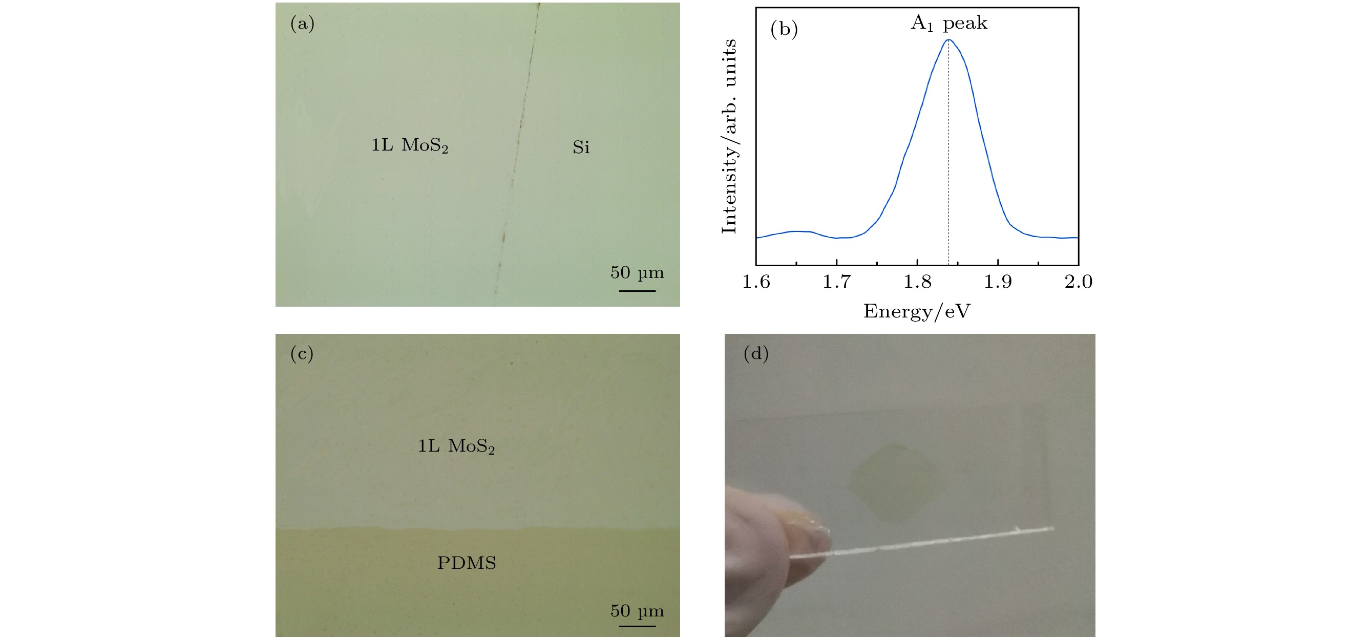
图 8 单层MoS2连续膜通过湿法转移后, (a)转移到Si衬底上的OM图像, (b)转移到Si衬底上的PL光谱, (c)转移到PDMS衬底上的OM图像, (d)转移到PDMS衬底上的实物图
Figure 8. (a) OM images transferred to Si substrates, (b) PL spectra transferred to Si substrates, (c) OM images transferred to PDMS substrates, (d) real figures transferred to PDMS substrates when monolayer MoS2 continuous film is transferred by wet method.
-
[1] Lin J, Zhong J, Zhong S, Li H, Zhang H, Chen W 2013 Appl. Phys. Lett. 103 063109
 Google Scholar
[2] Yin Z, Zhang X, Cai Y, Chen J, Wong J I, Tay Y Y 2014 Angew. Chem. Int. Ed. 53 12560
 Google Scholar
[3] Que H F, Jiang H N, Wang X G, Zhai P B, Meng L J, Zhang P, Gong Y J 2021 Acta Phys-Chim Sin. 37 2010051
 Google Scholar
[4] Kumar S, Sharma A, Tomar M, Gupta V 2021 Mater. Sci. Eng. B 266 11
 Google Scholar
[5] Tetsuka H, Nagoya A, Tamura S I 2016 Nanoscale 8 19677
 Google Scholar
[6] Singh E, Kim K S, Yeom G Y, Nalwa H S 2017 RSC Advan. 7 28234
 Google Scholar
[7] Pak S, Jang A R, Lee J, Hong J, Giraud P, Lee S 2019 Nanoscale 11 4726
 Google Scholar
[8] Liu Y, Weiss N O, Duan X D, Cheng H C, Huang Y, Duan X F 2016 Nat. Rev. Mater. 1 17
 Google Scholar
[9] Wu W, Wang L, Yu R, Liu Y, Wei S H, Hone J 2016 Advan. Mater. 28 8463
 Google Scholar
[10] Liu Z, Amani M, Najmaei S, Xu Q, Zou X, Zhou W 2014 Nat. Commun. 5 5246
 Google Scholar
[11] Pak S, Lee J, Jang A, Kim S, Park K, Sohn J I, Cha S 2020 Adv. Funct. Mater. 30 2002023
 Google Scholar
[12] Conley H J, Wang B, Ziegler J I, Haglund R F, Pantelides S T, Bolotin K I 2013 Nano Lett. 13 3626
 Google Scholar
[13] Dadgar A M, Scullion D, Kang K, Esposito D, Yang E H, Herman I P 2018 Chem. Mat. 30 5148
 Google Scholar
[14] 李明林, 万亚玲, 胡建玥, 王卫东 2016 物理学报 65 176201
 Google Scholar
Li M L, Wan Y L, Hu J Y, Wang W D 2016 Acta Phys. Sin. 65 176201
 Google Scholar
[15] Kuc A, Zibouch N E, Heine T 2011 Phys. Rev. B 83 245213
 Google Scholar
[16] 吴木生, 徐波, 刘刚, 欧阳楚英 2012 物理学报 61 227102
 Google Scholar
Wu M S, Xu B, Liu G, Ouyang C Y 2012 Acta Phys. Sin. 61 227102
 Google Scholar
[17] Wu J Y, Cao P Q, Zhang Z S, Ning F L, Zheng S S, He J Y, Zhang Z L 2018 Nano Lett. 18 1543
 Google Scholar
[18] Zhang R, Koutsos V, Cheung R 2016 Appl. Phys. Lett. 108 042104
 Google Scholar
[19] Hao S, Yang B, Gao Y 2017 Appl. Phys. Lett. 110 153105
 Google Scholar
[20] Yang Y, Li X, Wen M, Hacopian E, Chen W, Gong Y, Zhang J, Li B, Zhou W, Ajayan P M, Chen Q, Zhu T, Lou J 2017 Adv. Mater. 29 1604201
 Google Scholar
[21] Yun W S, Han S W, Hong S C, Kim I G, Lee J D 2012 Phys. Rev. B 85 033305
 Google Scholar
[22] Hu T, Li R, Dong J M 2013 J. Chem. Phys. 139 174702
 Google Scholar
[23] 徐波, 潘必才 2008 物理学报 57 6526
 Google Scholar
Xu B, Pan B C 2008 Acta Phys. Sin. 57 6526
 Google Scholar
[24] Kresse G, Furthmuller J 1996 Phys. Rev. B 54 11169
 Google Scholar
[25] Ramakrishna M, Gomathi A, Manna A K 2010 Angew. Chem. Int. Ed. 122 4153
 Google Scholar
[26] Kam K K, Parkinson B A 1982 J. Phys. Chem. 86 463
 Google Scholar
[27] Gajdos M, Hummer K, Kresse G 2006 Phys. Rev. B 73 045112
 Google Scholar
[28] Kadantsev E S, Hawrylak P 2012 Solid State Commun. 152 909
 Google Scholar
[29] Wang W D, Yang C G, Bai L W, Li M L, Li W B 2018 Nanomaterials 8 74
 Google Scholar
[30] Mak K F, He K, Lee C, Lee G H, Hone J, Heinz T F 2013 Nat. Mater. 12 207
 Google Scholar
Catalog
Metrics
- Abstract views: 12256
- PDF Downloads: 275
- Cited By: 0


 DownLoad:


