-
The AlOX tunnel barrier in Josephson junctions prepared by conventional thermal oxidation method is formed by diffusing high-purity oxygen into the surface of Al. But the tunnel barrier fabricated by this method is not completely oxidized, and the thickness of barrier is hard to control accurately. In this work, we use atomic layer deposition to grow Al2O3 tunnel barrier on the surface of Ti. The sandwich structure of Ti/Al2O3/Ti Josephson junction is grown layer by layer. We investigate the corresponding microstructure and electrical properties by adjusting the thickness of the Al2O3 tunnel barrier and the area of the junction. The experimental results show that the monolayer Al2O3 film is about 1.17 Å (1 Å = 10–10 m), which is grown by atomic layer deposition, achieves atomic-level controlled thickness. The resistance is controlled by adjusting the barrier thickness at room temperature. And we obtain a Josephson junction with good resistance uniformity at room temperature by optimizing the junction area.
-
Keywords:
- atomic layer deposition /
- Al2O3 tunnel barrier /
- Josephson junction /
- room temperature resistance
[1] 熊康林, 冯加贵, 郑亚锐, 崔江煜, 翁文康, 张胜誉, 李顺峰, 杨辉 2022 科学通报 67 143
 Google Scholar
Xiong K L, Feng J G, Zheng Y R, Cui J Y, Weng W K, Zhang S Y, Li S F, Yang H 2022 Chin. Sci. Bull. 67 143
 Google Scholar
[2] Abelson L A, Kerber G L 2004 Proc. IEEE. 92 1517
 Google Scholar
[3] Shapiro S 1963 Phys. Rev. Lett. 11 80
 Google Scholar
[4] Clarke J 1972 Phys. Rev. Lett. 28 1363
 Google Scholar
[5] Gurvitch M, Washington M A, Huggins H A 1983 Appl. Phys. Lett. 42 472
 Google Scholar
[6] Cai N, Zhou G W, Muller K, Starr D E 2012 Appl. Phys. Lett. 101 171605
 Google Scholar
[7] McDermottin R 2009 IEEE Trans. Appl. Supercond. 19 2
 Google Scholar
[8] Oh S, Cicak K, Kline J S, Sillanpaa M A, Osborn K D, Whittaker J D, Simmonds R W, Pappas D P 2006 Phys. Rev. B 74 100502
 Google Scholar
[9] George S M 2010 Chem. Rev. 110 111
 Google Scholar
[10] Geroge S M, Ott A W, Klaus J W 1996 J. Phys. Chem. 100 13121
 Google Scholar
[11] Dillon A C, Ott A W, Way J D, Geroge S M 1995 Surf. Sci. 322 230
 Google Scholar
[12] Ott A W, Klaus J W, Johnson J M, George S M 1997 Thin Solid Films 292 135
 Google Scholar
[13] Groner M D, Elam J W, Fabreguette F H, Gerogr S M 2002 Thin Solid Films 413 186
 Google Scholar
[14] Khalil M S, Stoutimore M J A, Gladchenko S, Holder A M, Musgrave C B, Kozen A C, Rubloff G, Liu Y Q, Gordon R G, Yum J H, Banerjee S K, Lobb C J, Osborn K D 2013 Appl. Phys. Lett. 103 162601
 Google Scholar
[15] Delavant M, Guillan J, Galpin D, Chhun S, Juhel M, Guiheux D, Jian P, Ha T H, Forster J, Guggilla S, Hong S, Bozon B 2012 Microelectron. Eng. 92 38
 Google Scholar
[16] Ambegaokar V, Baratoff A 1963 Phys. Rev. Lett. 10 486
 Google Scholar
[17] Steinbach A, Joyez P, Cottet A, Esteve D, Devoret M H, Huber M E, Martinis J M 2001 Phys. Rev. Lett. 87 137003
 Google Scholar
[18] Zhang E J, Srinivasan S, Sundaresan N, et al. 2020 arXiv: 2012.08475 [quant-ph]
[19] Osman A, Simon J, Bengtsson A, Kosen S, Krantz P, Lozano D P, Scigliuzzo M, Dlesing P, Bylander J, Roudsari A F 2021 Appl. Phys. Lett. 118 064002
 Google Scholar
[20] Verjauw J, Acharya R, Damme J V, et al. 2022 arXiv: 2202.10303 [quant-ph]
-
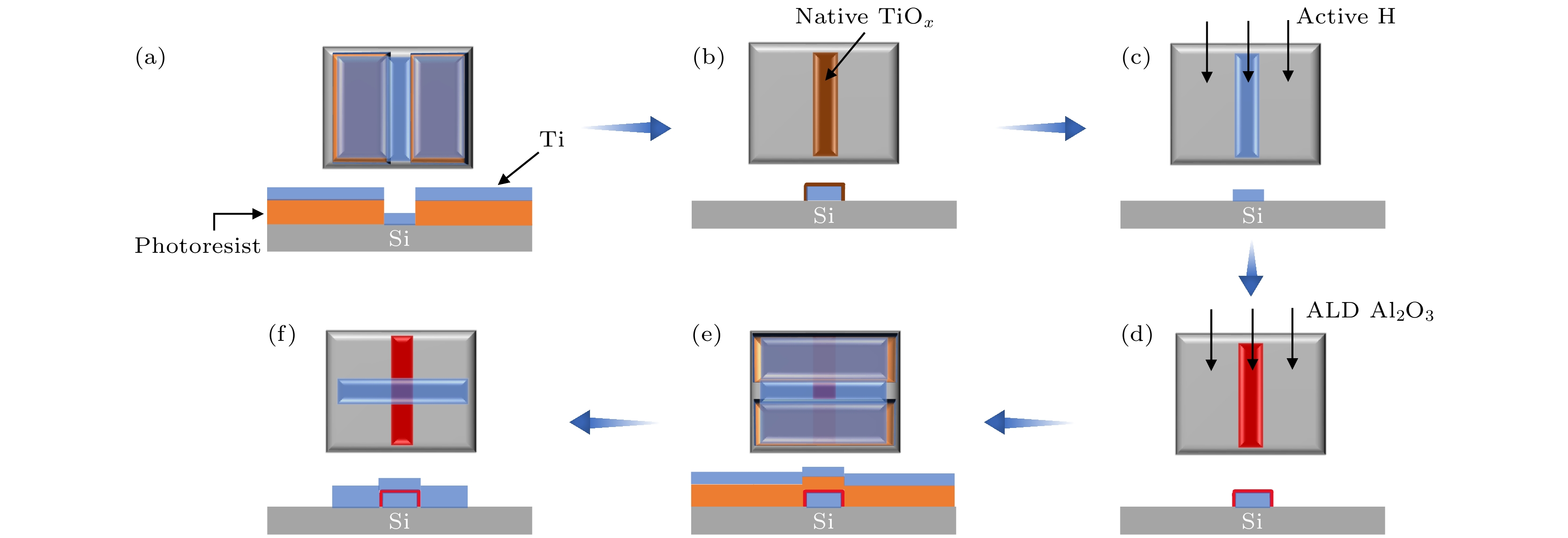
图 2 约瑟夫森结制备过程示意图 (a) 光刻后第一次溅射Ti示意图; (b) 光刻胶剥离后, Ti金属电极表面立即形成自然氧化层; (c) 使用RPC技术利用活性氢去除氧化层; (d) 去除自然氧化层后原位ALD 生长Al2O3; (e) 第二次光刻确定顶电极图案, 并进行第二次溅射Ti; (f) 金属剥离形成完整的结
Figure 2. Schematic diagram of Josephson junction preparation process: (a) Schematic diagram of the first sputtered Ti after photolithography; (b) natural oxide layer formed on the Ti metal electrode surface immediately after lift-off process; (c) removal of the oxide layer using the RPC technique by reactive hydrogen; (d) in situ ALD growth of Al2O3 after removal of the natural oxide layer; (e) the second photolithography to determine the top electrode pattern and sputtered Ti again; (f) lift-off process to complete the junction.
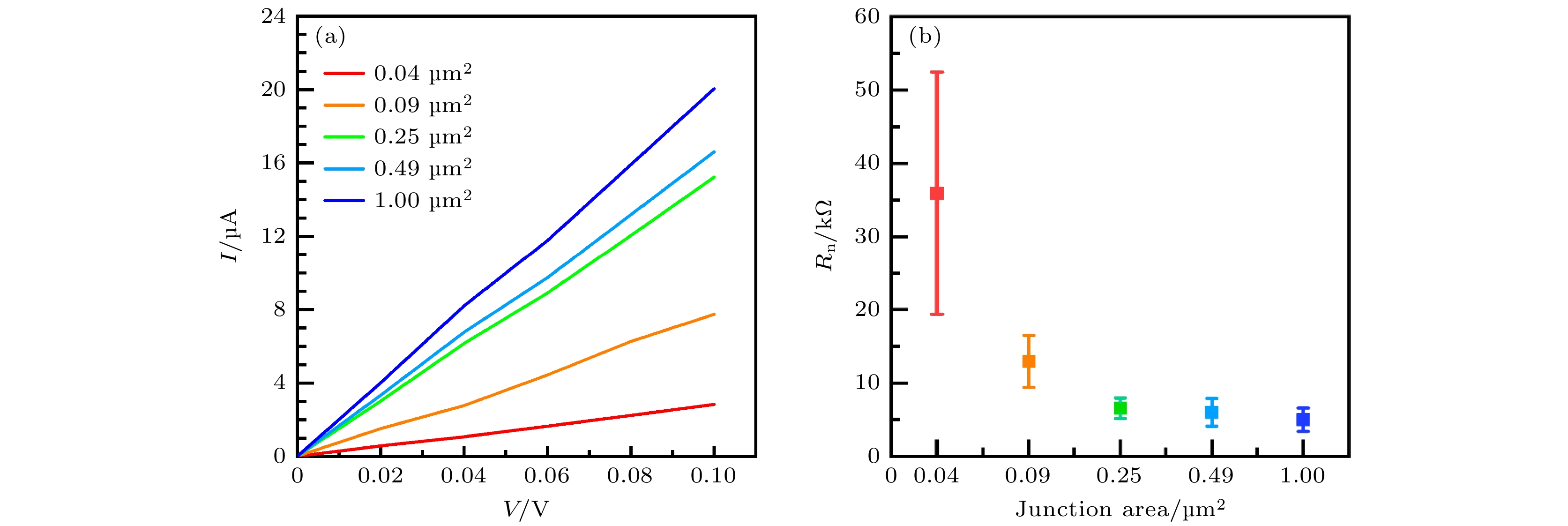
图 4 不同结面积下约瑟夫森结的室温电阻测量结果以及其均匀性数据图 (a) 室温下测量的不同结面积下约瑟夫森结的I-V曲线; (b) 结面积与电阻值之间的关系(图中点表示测量电阻的平均值, Y误差棒使用标准差计算)
Figure 4. Room temperature resistance measurements of Josephson junctions at different junction areas and their uniformity data plotted: (a) I-V curves of Josephson junctions at different junction areas measured at room temperature; (b) relationship between junction areas and resistance values (The dots in the graphs indicate the mean values of the measured resistances, and the Y error bars are calculated using the standard deviation).
表 1 不同结面积的约瑟夫森结室温电阻比较
Table 1. Comparison of room temperature resistance of Josephson junctions with different areas.
结面积/μm2 0.04 0.09 0.25 0.49 1.00 电阻平均值/kΩ 35.9 12.9 6.55 5.99 5.00 RSD/% 45.0 27.0 21.0 31.0 31.7 -
[1] 熊康林, 冯加贵, 郑亚锐, 崔江煜, 翁文康, 张胜誉, 李顺峰, 杨辉 2022 科学通报 67 143
 Google Scholar
Xiong K L, Feng J G, Zheng Y R, Cui J Y, Weng W K, Zhang S Y, Li S F, Yang H 2022 Chin. Sci. Bull. 67 143
 Google Scholar
[2] Abelson L A, Kerber G L 2004 Proc. IEEE. 92 1517
 Google Scholar
[3] Shapiro S 1963 Phys. Rev. Lett. 11 80
 Google Scholar
[4] Clarke J 1972 Phys. Rev. Lett. 28 1363
 Google Scholar
[5] Gurvitch M, Washington M A, Huggins H A 1983 Appl. Phys. Lett. 42 472
 Google Scholar
[6] Cai N, Zhou G W, Muller K, Starr D E 2012 Appl. Phys. Lett. 101 171605
 Google Scholar
[7] McDermottin R 2009 IEEE Trans. Appl. Supercond. 19 2
 Google Scholar
[8] Oh S, Cicak K, Kline J S, Sillanpaa M A, Osborn K D, Whittaker J D, Simmonds R W, Pappas D P 2006 Phys. Rev. B 74 100502
 Google Scholar
[9] George S M 2010 Chem. Rev. 110 111
 Google Scholar
[10] Geroge S M, Ott A W, Klaus J W 1996 J. Phys. Chem. 100 13121
 Google Scholar
[11] Dillon A C, Ott A W, Way J D, Geroge S M 1995 Surf. Sci. 322 230
 Google Scholar
[12] Ott A W, Klaus J W, Johnson J M, George S M 1997 Thin Solid Films 292 135
 Google Scholar
[13] Groner M D, Elam J W, Fabreguette F H, Gerogr S M 2002 Thin Solid Films 413 186
 Google Scholar
[14] Khalil M S, Stoutimore M J A, Gladchenko S, Holder A M, Musgrave C B, Kozen A C, Rubloff G, Liu Y Q, Gordon R G, Yum J H, Banerjee S K, Lobb C J, Osborn K D 2013 Appl. Phys. Lett. 103 162601
 Google Scholar
[15] Delavant M, Guillan J, Galpin D, Chhun S, Juhel M, Guiheux D, Jian P, Ha T H, Forster J, Guggilla S, Hong S, Bozon B 2012 Microelectron. Eng. 92 38
 Google Scholar
[16] Ambegaokar V, Baratoff A 1963 Phys. Rev. Lett. 10 486
 Google Scholar
[17] Steinbach A, Joyez P, Cottet A, Esteve D, Devoret M H, Huber M E, Martinis J M 2001 Phys. Rev. Lett. 87 137003
 Google Scholar
[18] Zhang E J, Srinivasan S, Sundaresan N, et al. 2020 arXiv: 2012.08475 [quant-ph]
[19] Osman A, Simon J, Bengtsson A, Kosen S, Krantz P, Lozano D P, Scigliuzzo M, Dlesing P, Bylander J, Roudsari A F 2021 Appl. Phys. Lett. 118 064002
 Google Scholar
[20] Verjauw J, Acharya R, Damme J V, et al. 2022 arXiv: 2202.10303 [quant-ph]
Catalog
Metrics
- Abstract views: 8803
- PDF Downloads: 195
- Cited By: 0


 DownLoad:


