


-
Stacking two-dimensional materials into heterogeneous structures is an effective strategy to regulate their physical properties and enrich their applications in modern nanoelectronics. The electronic structure and optical properties of a new two-dimensional Janus Ga2SeTe/In2Se3 heterojunction with four stacked configurations are investigated by first principles calculations. The heterojunction of the four configurations is an indirect band-gap semiconductor with a type-II band structure, and the photoelectron donor and acceptor materials are determined by the polarization direction of two-dimensional In2Se3. The light absorption rises to 25% in the visible region, which is conducive to the effective utilization of the solar visible light. The biaxial strain can induce direct-indirect bandgap transition, and the applied electric field can effectively regulate the bandgap of heterogeneous structure. The bandgap of AA2 configuration increases monotonically from 0.195 eV to 0.714 eV, but that of AB2 configuration decreases monotonically from 0.859 eV to 0.058 eV. The band of the heterojunction always maintains the type-II structure under the two kinds of configurations. The heterojunctions under compressive strain show better light absorption capability in the visible region with shorter wavelength. These results reveal the regulatory mechanism of the Janus Ga2SeTe/In2Se3 van der Waals heterojunction electronic structure and provide theoretical guidance in designing novel optoelectronic devices.
-
Keywords:
- Janus single layer /
- Van der Waals heterojunction /
- photoelectric characteristics /
- first principles
[1] Butler S Z, Hollen S M, Cap L, et al. 2013 ACS Nano 7 2898
 Google Scholar
[2] Das S, Robinson J A, Dubey M, et al. 2015 Annu. Rev. Mater. Res. 45 1
Google Scholar
[3] Zhu B, Zhang X, Zeng B, et al. 2017 Org. Electron. 49 45
Google Scholar
[4] OuYang F P, Xu H, Fan T 2007 J. Appl. Phys. 102 064501
Google Scholar
[5] Chen J Y, Li X X, Zhou W Z, et al. 2020 Adv. Electron. Mater. 6 1900490
Google Scholar
[6] Neto A H C, Guinea F, Peres N M R, et al. 2009 Rev. Mod. Phys. 81 109
Google Scholar
[7] OuYang F P, Xu Hui, Wei Chen 2008 Acta Phys. Sin. Ch. Ed. 57 1073
Google Scholar
[8] Feng B J, Ding Z J, Meng S, et al. 2012 Nano Lett. 12 3507
Google Scholar
[9] Qiao J, Kong X, Hu Z X, et al. 2014 Nat. Commun. 5 4475
Google Scholar
[10] Xiao J, Long M Q, Li X M, et al. 2014 J. Phys. Condens. Matter 26 405302
Google Scholar
[11] Zhu P, Chen Y, Zhou Y, et al. 2018 Int. J. Hydrog. Energy 43 14087
Google Scholar
[12] Wu D, Shi J, Zheng X, et al. 2019 Phys. Status Solidi Rapid Res. Lett. 13 1900063
Google Scholar
[13] Zhu J, Ha E, Zhao G L, et al. 2017 Coord. Chem. Rev. 352 306
Google Scholar
[14] Ouyang F P, Ni X, Yang Z X, et al. 2013 J. Appl. Phys. 114 213701
Google Scholar
[15] Hu Y, Zhang S, Sun S, et al. 2015 Appl. Phys. Lett. 107 122107
Google Scholar
[16] Guo G, Shi Y, Zhang Y, et al. 2020 Comput. Mater. Sci. 172 109348
Google Scholar
[17] Chen L N, OuYang F P, Ma S S, et al. 2010 Phys. Lett. A 374 4343
Google Scholar
[18] Xiao J, Yang Z X, Xie W T, et al. 2012 Chin. Phys. B 21 027102
Google Scholar
[19] Zhou W Z, Yang Z X, Li A L, et al. 2020 Phys. Rev. B 101 045113
Google Scholar
[20] Chen H, Li Y, Huang L, et al. 2015 J. Phys. Chem. C 119 29148
Google Scholar
[21] Long R, Prezhdo O. V 2016 Nano Lett. 16 1996
Google Scholar
[22] Ahmad W, Liu J, Jiang J, et al. 2021 Adv. Funct. Mater. 31 2104143
Google Scholar
[23] Geim, Andre K, Grigorieva I V 2013 Nature 499 419
Google Scholar
[24] Novoselov K S, Mishchenko A, Carvalho A, et al. 2016 Science 353 aac9439
Google Scholar
[25] Zhu Z, Zhang B, Chen X, et al. 2020 Appl. Phys. Lett. 117 082902
Google Scholar
[26] Almayyali, Ali Obies Muhsen, Bahjat B Kadhim, et al. 2020 Chem. Phys. 532 110679
Google Scholar
[27] Shang J, Pan L, Wang X, et al. 2018 J. Mater. Chem. C 6 7201
Google Scholar
[28] Ding W J, Zhu J B, Wang Z, et al. 2017 Nat. Commun. 8 14956
Google Scholar
[29] Hu L, Huang X 2017 RSC Adv. 7 55034
Google Scholar
[30] Chen Y, Tang Z, Shan H, et al. 2021 Phys. Rev. B 104 075449
Google Scholar
[31] Duan X, Tang S, Huang Z 2021 Comput. Mater. Sci. 200 110819
Google Scholar
[32] Li R, Li L, Cheng Y, et al. 2018 Small 14 1802091
Google Scholar
[33] Ibarra-Hernández W, Elsayed H, Romero A H, et al. 2017 Phys. Rev. B 96 035201
Google Scholar
[34] Kandemir A, Sahin H 2018 Phys. Rev. B 97 155410
Google Scholar
[35] Guo Y, Zhou S, Bai Y, et al. 2017 Appl. Phys. Lett. 110 163102
Google Scholar
[36] Bui H D, Jappor H R, Hieu N N 2019 Superlattices Microstruct. 125 1
Google Scholar
[37] Singh S, Choudhary S 2022 Eur. Phys. J. D 76 1
Google Scholar
[38] Min J, Zhou M, Zhang C, et al. 2021 Phys. Lett. A 413 127594
Google Scholar
[39] Kresse G, Furthmüller J 1996 Comput. Mater. Sci. 6 15
Google Scholar
[40] Kresse G, Furthmüller J, Hafner J 1994 Phys. Rev. B 50 13181
Google Scholar
[41] Perdew J P, Burke K, Ernzerhof M 1996 Phys. Rev. Lett. 77 3865
Google Scholar
[42] Kerber T, Sierka M, Sauer J 2008 J. Comput. Chem. 29 2088
Google Scholar
[43] Grimme S 2006 J. Comput. Chem. 27 1787
Google Scholar
[44] Monkhorst H J, Pack J D 1976 Phys. Rev. B 13 5188
Google Scholar
[45] Bernardi M, Palummo M, Grossman J C 2013 Nano Lett. 13 3664
Google Scholar
[46] Huang B, Deng H X, Lee H, et al. 2014 Phys. Rev. X 4 021029
[47] Shi G, Kioupakis E 2015 Nano Lett. 15 6926
Google Scholar
[48] Tao X, Gu Y 2013 Nano Lett. 13 3501
Google Scholar
[49] Zhang W X, Shi C H, He C, et al. 2020 J. Solid State Chem. 289 121511
Google Scholar
[50] Li X, Zhai B, Song X, et al. 2020 Appl. Surf. Sci. 509 145317
Google Scholar
-

图 1 (a) 二维Janus Ga2SeTe的俯视图(上)和侧视图(下); (b) 二维In2Se3的俯视图(上)和侧视图(下); (c) 二维Janus Ga2SeTe的能带结构图; (d) 二维In2Se3的能带结构图
Figure 1. (a) Top view (upper) and side view (lower) of 2 D Janus Ga2SeTe; (b) top view (upper) and side view (lower) of 2 D In2Se3; (c) the energy band structure diagram of two-dimensional Janus Ga2SeTe; (d) energy band structure diagram of two-dimensional In2Se3.
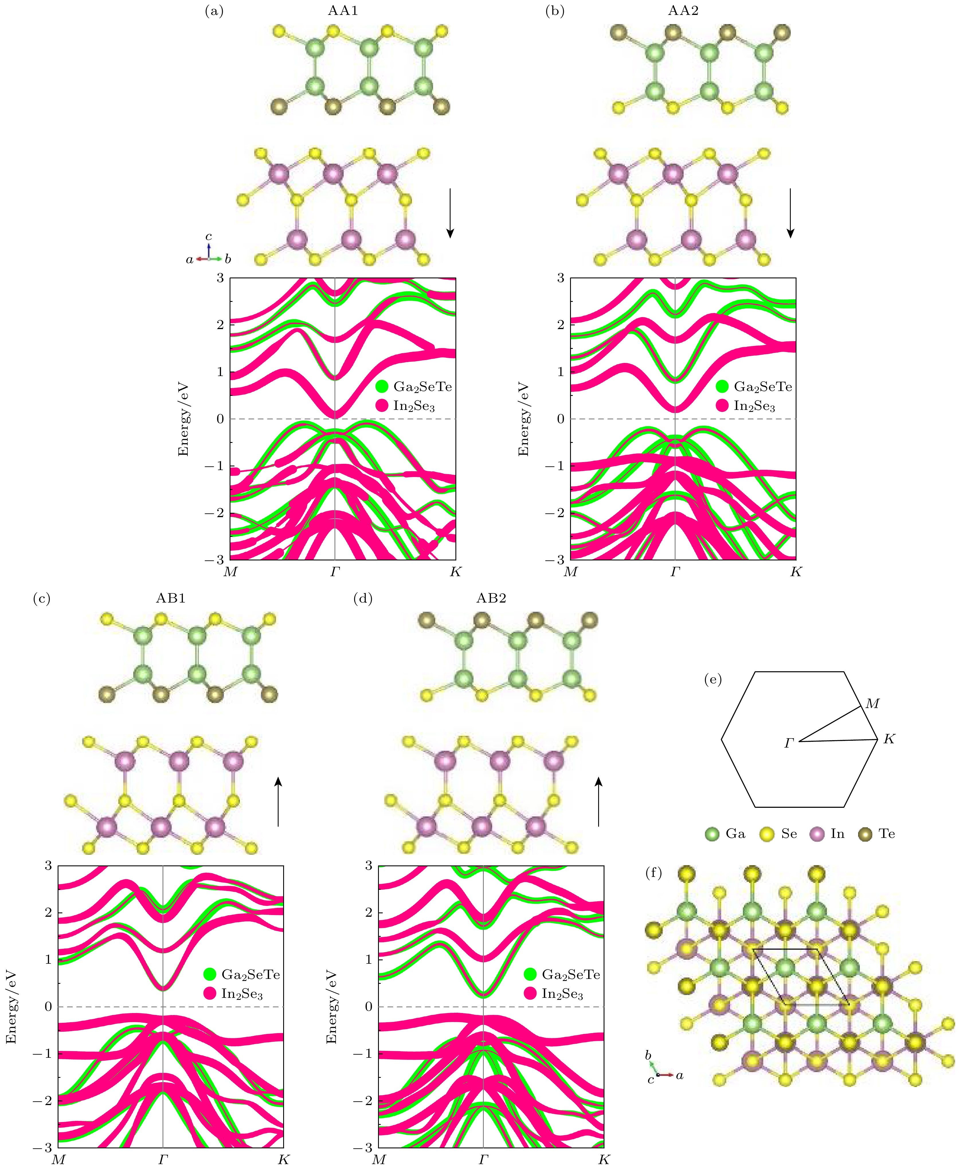
图 2 4种堆叠构型 (a) AA1, (b) AA2, (c) AB1, (d) AB2结构侧视图(上)及能带结构(下), 其中绿色为Ga2SeTe的贡献, 红色为In2Se3的贡献; (e) 相应的布里渊区和高对称点; (f)Janus Ga2SeTe/In2Se3异质结俯视图
Figure 2. The structure side view (top) and band structure (bottom) of four stack configurations (a )AA1, (b) AA2, (c) AB1 and (d) AB2, Green is the contribution of Ga2SeTe and red is In2Se3. (e) Corresponding Brillouin zones and points of high symmetry; (f) top view of Janus Ga2SeTe/In2Se3 heterojunction.

图 3 单层Ga2SeTe、单层In2Se3、 Janus Ga2SeTe/In2Se3异质结 (a) AA1; (b) AA2; (c) AB1; (d) AB2堆叠构型的能带对齐图
Figure 3. Band alignment of single-layer Ga2SeTe, single-layer In2Se3, Janus Ga2SeTe/In2Se3 heterojunction (a) AA1; (b) AA2; (c) AB1; (d) AB2 stack configurations.

图 4 (a) Janus Ga2SeTe/In2Se3异质结AA1, AA2, AB1, AB2堆叠构型、单层Ga2SeTe、单层In2Se3的光吸收度; (b) 局部放大图
Figure 4. (a) The light absorption of Janus Ga2SeTe/In2Se3 heterojunction AA1, AA2, AB1, AB2 stacking configuration, monolayer Ga2SeTe, monolayer In2Se3; (b) partial magnification.
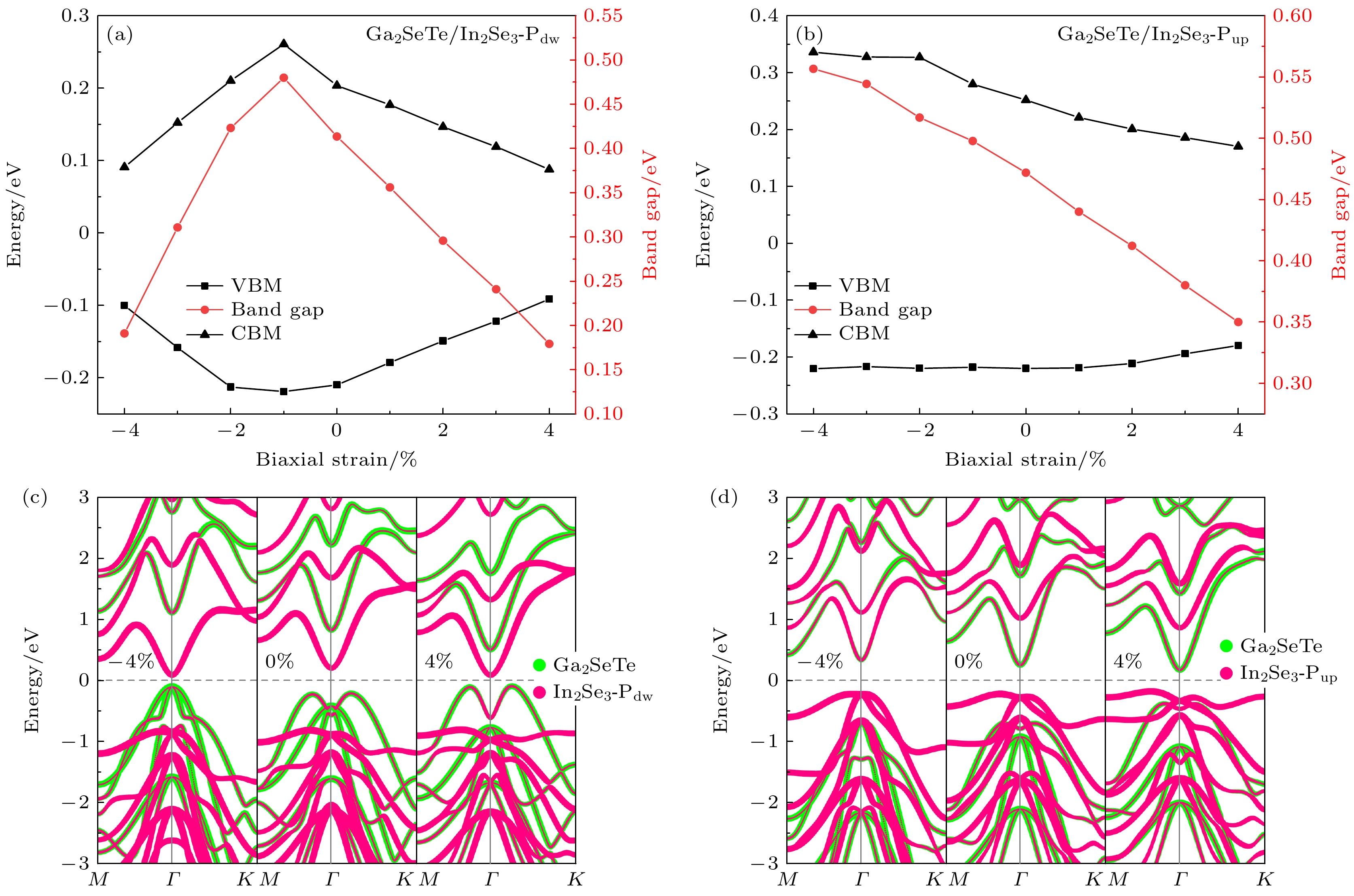
图 5 Janus Ga2SeTe/In2Se3异质结 (a) AA2, (b) AB2堆叠构型CBM、VBM和带隙与双轴应变的函数关系图; 双轴应变下(c) AA2, (d) AB2堆叠构型的能带结构
Figure 5. Function of Janus Ga2SeTe/In2Se3 heterojunction (a) AA2, (b) AB2 stacked configuration CBM, VBM and Band gap with biaxial strain; band structure of (c) AA2, (d) AB2 stacked configuration under biaxial strain.
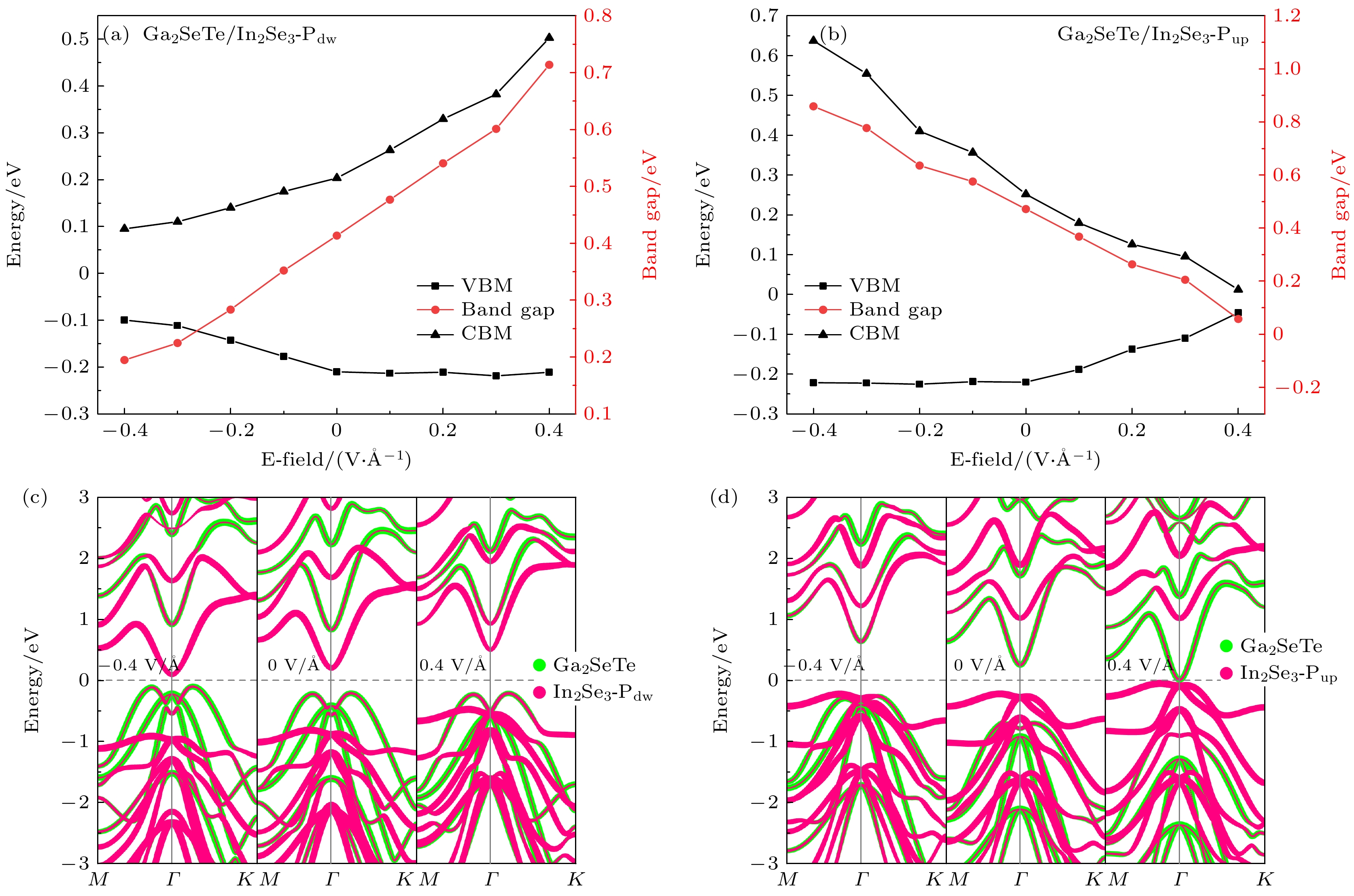
图 6 Janus Ga2SeTe/In2Se3异质结 (a) AA2, (b) AB2堆叠构型CBM, VBM和带隙与外加电场的函数关系图, 外加电场下(c) AA2, (d) AB2堆叠构型的能带结构
Figure 6. Function of Janus Ga2SeTe/In2Se3 heterojunction (a) AA2, (b) AB2 stacked configuration CBM, VBM and band gap with external electric field, band structure of (c) AA2, (d) AB2 stacked configuration under external electric field.

图 7 双轴应变为–4%, 0%, 4%下Janus Ga2SeTe/In2Se3异质结 (a) AA2, (b) AB2堆叠构型的光吸收度; 外加电场为–0.4, 0, 0.4 V/Å下Ga2SeTe/In2Se3异质结(c) AA2, (d) AB2堆叠构型的光吸收度
Figure 7. The light absorption of Janus Ga2SeTe/In2Se3 heterojunction (a) AA2, (b) AB2 stack configuration under biaxial strain of –4%, 0% and 4%. The optical absorption of Ga2SeTe/In2Se3 heterojunction (c) AA2, (d) AB2 stack configuration under applied electric field of –0.4, 0, 0.4 V/Å.
表 1 4种Janus Ga2SeTe/In2Se3范德瓦耳斯异质结的Eb和带隙(Eg)
Table 1. Eb and band gap (Eg) of four Janus Ga2SeTe/In2Se3 Van der Waals heterojunctions.
AA1 AA2 AB1 AB2 Eb/eV –2.404 –2.380 –2.392 –2.367 Eg/eV 0.184 0.414 0.611 0.472  DownLoad: CSV
-
[1] Butler S Z, Hollen S M, Cap L, et al. 2013 ACS Nano 7 2898
Google Scholar
[2] Das S, Robinson J A, Dubey M, et al. 2015 Annu. Rev. Mater. Res. 45 1
Google Scholar
[3] Zhu B, Zhang X, Zeng B, et al. 2017 Org. Electron. 49 45
Google Scholar
[4] OuYang F P, Xu H, Fan T 2007 J. Appl. Phys. 102 064501
Google Scholar
[5] Chen J Y, Li X X, Zhou W Z, et al. 2020 Adv. Electron. Mater. 6 1900490
Google Scholar
[6] Neto A H C, Guinea F, Peres N M R, et al. 2009 Rev. Mod. Phys. 81 109
Google Scholar
[7] OuYang F P, Xu Hui, Wei Chen 2008 Acta Phys. Sin. Ch. Ed. 57 1073
Google Scholar
[8] Feng B J, Ding Z J, Meng S, et al. 2012 Nano Lett. 12 3507
Google Scholar
[9] Qiao J, Kong X, Hu Z X, et al. 2014 Nat. Commun. 5 4475
Google Scholar
[10] Xiao J, Long M Q, Li X M, et al. 2014 J. Phys. Condens. Matter 26 405302
Google Scholar
[11] Zhu P, Chen Y, Zhou Y, et al. 2018 Int. J. Hydrog. Energy 43 14087
Google Scholar
[12] Wu D, Shi J, Zheng X, et al. 2019 Phys. Status Solidi Rapid Res. Lett. 13 1900063
Google Scholar
[13] Zhu J, Ha E, Zhao G L, et al. 2017 Coord. Chem. Rev. 352 306
Google Scholar
[14] Ouyang F P, Ni X, Yang Z X, et al. 2013 J. Appl. Phys. 114 213701
Google Scholar
[15] Hu Y, Zhang S, Sun S, et al. 2015 Appl. Phys. Lett. 107 122107
Google Scholar
[16] Guo G, Shi Y, Zhang Y, et al. 2020 Comput. Mater. Sci. 172 109348
Google Scholar
[17] Chen L N, OuYang F P, Ma S S, et al. 2010 Phys. Lett. A 374 4343
Google Scholar
[18] Xiao J, Yang Z X, Xie W T, et al. 2012 Chin. Phys. B 21 027102
Google Scholar
[19] Zhou W Z, Yang Z X, Li A L, et al. 2020 Phys. Rev. B 101 045113
Google Scholar
[20] Chen H, Li Y, Huang L, et al. 2015 J. Phys. Chem. C 119 29148
Google Scholar
[21] Long R, Prezhdo O. V 2016 Nano Lett. 16 1996
Google Scholar
[22] Ahmad W, Liu J, Jiang J, et al. 2021 Adv. Funct. Mater. 31 2104143
Google Scholar
[23] Geim, Andre K, Grigorieva I V 2013 Nature 499 419
Google Scholar
[24] Novoselov K S, Mishchenko A, Carvalho A, et al. 2016 Science 353 aac9439
Google Scholar
[25] Zhu Z, Zhang B, Chen X, et al. 2020 Appl. Phys. Lett. 117 082902
Google Scholar
[26] Almayyali, Ali Obies Muhsen, Bahjat B Kadhim, et al. 2020 Chem. Phys. 532 110679
Google Scholar
[27] Shang J, Pan L, Wang X, et al. 2018 J. Mater. Chem. C 6 7201
Google Scholar
[28] Ding W J, Zhu J B, Wang Z, et al. 2017 Nat. Commun. 8 14956
Google Scholar
[29] Hu L, Huang X 2017 RSC Adv. 7 55034
Google Scholar
[30] Chen Y, Tang Z, Shan H, et al. 2021 Phys. Rev. B 104 075449
Google Scholar
[31] Duan X, Tang S, Huang Z 2021 Comput. Mater. Sci. 200 110819
Google Scholar
[32] Li R, Li L, Cheng Y, et al. 2018 Small 14 1802091
Google Scholar
[33] Ibarra-Hernández W, Elsayed H, Romero A H, et al. 2017 Phys. Rev. B 96 035201
Google Scholar
[34] Kandemir A, Sahin H 2018 Phys. Rev. B 97 155410
Google Scholar
[35] Guo Y, Zhou S, Bai Y, et al. 2017 Appl. Phys. Lett. 110 163102
Google Scholar
[36] Bui H D, Jappor H R, Hieu N N 2019 Superlattices Microstruct. 125 1
Google Scholar
[37] Singh S, Choudhary S 2022 Eur. Phys. J. D 76 1
Google Scholar
[38] Min J, Zhou M, Zhang C, et al. 2021 Phys. Lett. A 413 127594
Google Scholar
[39] Kresse G, Furthmüller J 1996 Comput. Mater. Sci. 6 15
Google Scholar
[40] Kresse G, Furthmüller J, Hafner J 1994 Phys. Rev. B 50 13181
Google Scholar
[41] Perdew J P, Burke K, Ernzerhof M 1996 Phys. Rev. Lett. 77 3865
Google Scholar
[42] Kerber T, Sierka M, Sauer J 2008 J. Comput. Chem. 29 2088
Google Scholar
[43] Grimme S 2006 J. Comput. Chem. 27 1787
Google Scholar
[44] Monkhorst H J, Pack J D 1976 Phys. Rev. B 13 5188
Google Scholar
[45] Bernardi M, Palummo M, Grossman J C 2013 Nano Lett. 13 3664
Google Scholar
[46] Huang B, Deng H X, Lee H, et al. 2014 Phys. Rev. X 4 021029
[47] Shi G, Kioupakis E 2015 Nano Lett. 15 6926
Google Scholar
[48] Tao X, Gu Y 2013 Nano Lett. 13 3501
Google Scholar
[49] Zhang W X, Shi C H, He C, et al. 2020 J. Solid State Chem. 289 121511
Google Scholar
[50] Li X, Zhai B, Song X, et al. 2020 Appl. Surf. Sci. 509 145317
Google Scholar

 DownLoad:
Catalog
Metrics
- Abstract views: 8641
- PDF Downloads: 196
- Cited By: 0
