Most Cited

2024, 73 (1): 010301.
doi: 10.7498/aps.73.20231795
Abstract +
In the early decades of the 20th century, the inception of quantum mechanics catalyzed the first quantum revolution, resulting in groundbreaking technological advances, such as nuclear energy, semiconductors, lasers, nuclear magnetic resonance, superconductivity, and global satellite positioning systems. These innovations have promoted significant progress in material civilization, fundamentally changed the way of life and societal landscape of humanity. Since the 1990s, quantum control technology has made significant strides forward, ushering in a rapid evolution of quantum technologies, notably exemplified by quantum information science. This encompasses domains such as quantum communication, quantum computing, and quantum precision measurement, offering paradigm-shifting solutions for enhancing information transmission security, accelerating computational speed, and elevating measurement precision. These advances hold the potential to provide crucial underpinning for national security and the high-quality development of the national economy. The swift progression of quantum information technology heralds the advent of the second quantum revolution. Following nearly three decades of concerted efforts, China’s quantum information technology field as a whole has achieved a leap. Specifically, China presently assumes a prominent international role in both the research and practical application of quantum communication, leading the global domain in quantum computing, and achieving international preeminence or advanced standing across various facets of quantum precision measurement. Presently, it is imperative to conduct a comprehensive assessment of the developmental priorities in the realm of quantum information in China for the forthcoming 5 to 10 years, in alignment with national strategic priorities and the evolving landscape of international competition. This will enable the proactive establishment of next-generation information technology systems that are secure, efficient, autonomous, and controllable.
2024, 73 (3): 037201.
doi: 10.7498/aps.73.20231151
Abstract +
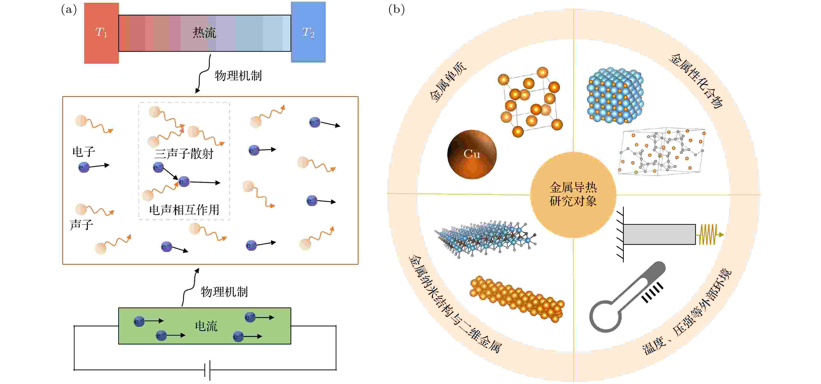
Metal is one of the most widely used engineering materials. In contrast to the extensive research dedicated to their mechanical properties, studies on the thermal conductivity of metals remain relatively rare. The understanding of thermal transport mechanisms in metals is mainly through the Wiedemann-Franz Law established more than a century ago. The thermal conductivity of metal is related to both the electron transport and the lattice vibration. An in-depth understanding of the thermal transport mechanism in metal is imperative for optimizing their practical applications. This review first discusses the history of the thermal transport theory in metals, including the Wiedemann-Franz law and models for calculating phonon thermal conductivity in metal. The recently developed first-principles based mode-level electron-phonon interaction method for determining the thermal transport properties of metals is briefly introduced. Then we summarize recent theoretical studies on the thermal conductivities of elemental metals, intermetallics, and metallic ceramics. The value of thermal conductivity, phonon contribution to total thermal conductivity, the influence of electron-phonon interaction on thermal transport, and the deviation of the Lorenz number are comprehensively discussed. Moreover, the thermal transport properties of metallic nanostructures are summarized. The size effect of thermal transport and the Lorenz number obtained from experiments and calculations are compared. Thermal transport properties including the phonon contribution to total thermal conductivity and the Lorenz number in two-dimensional metals are also mentioned. Finally, the influence of temperature, pressure, and magnetic field on thermal transport in metal are also discussed. The deviation of the Lorenz number at low temperatures is due to the different electron-phonon scattering mechanisms for thermal and electrical transport. The mechanism for the increase of thermal conductivity in metals induced by pressure varies in different kinds of metals and is related to the electron state at the Fermi level. The effect of magnetic field on thermal transport is related to the coupling between the electron and the magnetic field, therefore the electron distribution in the Brillouin zone is an important factor. In addition, this review also looks forward to the future research directions of metal thermal transport theory.

2024, 73 (19): 198901.
doi: 10.7498/aps.73.20240702
Abstract +
Supply chain is a chain structure formed by the sequential processes of production and distribution, spanning from raw material suppliers to end customers. An efficient and reliable supply chain is of great significance in enhancing enterprise’s market competitiveness and promoting sustainable social and economic development. The supply chain includes the interconnected flows of materials, resources, capital, and information across various stages, including procurement, production, warehousing, distribution, customer service, information management, and financial management. By representing the various participants in the supply chain as nodes and their interactions—such as the logistics, capital flow, information flow, and other interactions—as edges, the supply chain can be described and characterized as a complex network. In recent years, using complex network theory and methods to model and analyze supply chains has attracted increasing attention from researchers. This paper systematically reviews the supply chain research based on complex network theory, providing an in-depth analysis of supply chain networks in terms of network construction, structural properties, and management characteristics. First, this paper reviews two kinds of approaches to constructing supply chain network: empirical data-based approach and network model-based approach. In the empirical data-based research, scholars use common supply chain databases or integrate multiple data sources to identify the supply chain participants and clarify their attributes, behaviors, and interactions. Alternatively, the research based on network models employs the Barabási–Albert (BA) model, incorporating factors such as node distance, fitness, and edge weights, or uses hypergraph models to construct supply chain networks. Next, this paper summarizes the research on the structural properties of supply chain networks, focusing on their topological structure, key node identification, community detection, and vulnerability analysis. Relevant studies explore the topological structure of supply chain networks, uncovering the connections between nodes, hierarchical structures, and information flow paths between nodes. By analyzing factors such as node centrality, connection strength, and flow paths, the key nodes within the supply chain network are identified. Community detection algorithms are used to investigate the relationships between different structural parts and to analyze the positional structure, cooperative relationships, and interaction modes. Furthermore, quantitative evaluation indicators and management strategies are proposed for the robustness and resilience of supply chain networks. Further research has explored the management characteristics of supply chain networks, including risk propagation and competition game. Relevant studies have employed three main methods—epidemic model, cascading failure model, and agent-based model—to construct risk propagation models, simulate the spread of disruption risks, and analyze the mechanisms, paths, and extent of risk propagation within supply chain networks. These studies provide valuable insights for developing risk prevention and mitigation strategies. In addition, the game theory has been used to investigate the cooperative competition, resource allocation, and strategy selection among enterprises within the supply chain network. This paper reviews the research contents and emerging trends in supply chain studies based on complex network methods. It demonstrates the effectiveness and applicability of complex network theory in supply chain network research, discusses key challenges, such as how to obtain accurate, comprehensive, and timely supply chain network data, proposes standardized data processing methods, and determines the attributes of supply chain network nodes and the strength of their relationships. Furthermore, research on the structure of supply chain network has not yet fully captured the unique characteristics of supply chain networks. Existing models and methods for vulnerability assessment often fail to consider the dynamic and nonlinear characteristics of supply chain networks. Research on risk propagation in supply chains has not sufficiently integrated empirical data, overlooking the diversity of risk sources and the complexity of propagation paths. The asymmetry and incompleteness of information in supply chain networks, as well as multiple sources of uncertainty, make the prediction and analysis of multi-party decision-making behavior more complex. This paper also outlines several key directions for future research. One direction involves using high-order network theory to model interactions among multiple nodes and to describe the dynamics of multi-agent interactions within supply chain networks. Furthermore, integrating long short-term memory (LSTM) methods to process long-term dependence in time-series data can enhance the analysis of network structure evolution and improve the prediction of future states. The application of reinforcement learning algorithms can also adaptively adjust network structures and strategies according to changing conditions and demands, thereby improving the adaptability and response speed of supply chain networks in emergency situations. This paper aims to provide valuable insights for supplying chain research and promoting the development and application of complex network methods in this field.

2024, 73 (6): 063101.
doi: 10.7498/aps.73.20231631
Abstract +
Perovskite solar cell material becomes one of the most attractive light absorbing materials in the photovolatic field due toits unique photoelectric characteristics, especially the rapid improvement of photoelectric conversion efficiency in the initial short period of time. However, in recent years, the growth of conversion efficiency has entered a slow stage, posing a challenge for subsequent development. In addition, the long-time stability of material has become a key barrier to widespread commerical applications. The emergence of these problems is closely related to the inevitable defects in the material in preparation process, because defect is usually regarded as one of the key factors hindering the improvement of photovolatic performance and materical stability. Therefore, a comprehensive understanding of the inherent defects of material is essential to improve cell efficiency and maintain long-time structural stability. In this paper, the effects of defects in perovskite material on photovolatic performance and stability are discussed in many aspects, including the traditional rigid defects, unconventional defects, complex defects, and ion migration. Second, this work also delves into how defects affect carrier lifetime and highlights their role in determining the overall cell performance. Such insights are very important in designing effective strategies to mitigate the adverse effects of defects on material performance and stability. Finally, we discuss the complex relationship between defects and structural stability, and recognize that the defects are a key factor affecting the long-term robustness of perovskite solar cells. The understanding of the mechanism behind the focus problems will help researchers achieve new ideas to improve the efficiency and duraibility of perovskite solar cell technology. Overall, this review not only provides the current state of knowledge on defects in perovskite materials, but also illustrates further research directions. By revealing the complex interplay between defects, photovoltaic performance and structural stability, researchers can find a way to break through the current limitations and realize the potential value of perovskite solar cell technology in the commercial applications. Thiswork aims to spark an in-depth discussion of this issue and further explore and innovate in this promising field.
2024, 73 (7): 078801.
doi: 10.7498/aps.73.20240201
Abstract +
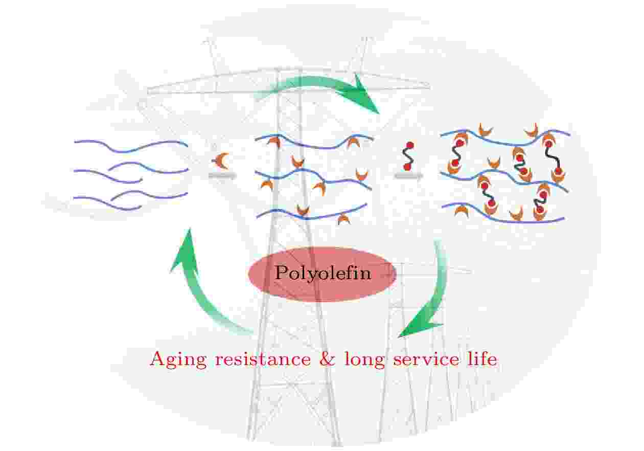
Cross-linked polyethylene (XLPE) has been widely used in the field of power cables due to its excellent mechanical properties and insulating properties. However, during the manufacturing of high voltage cables, XLPE will inevitably be affected by electrical aging, thermal aging and electro-thermal combined aging, which makes the resistance and life of the material decline. Therefore, it is necessary to enhance the aging resistance of XLPE without affecting its mechanical properties and insulating properties, so as to extend its service life. In this work, the structural characteristics and cross-linking mechanism of XLPE are introduced, the aging process and influencing mechanism are systematically analyzed, and the life decay problems of XLPE due to aging are explored by using methods such as the temperature Arrhenius equation and the inverse power law of voltage. The improvement strategies such as grafting, blending, and nanoparticle modification can be used to enhance the thermal stability, antioxidant properties, and thermal aging resistance of XLPE, thereby extending its service life. Finally, the strategies of adjusting and controlling the service life of XLPE cable insulation materials in the future are discussed, which provide theoretical guidance for further improving long-term stable operation of XLPE cable insulation materials.
2024, 73 (6): 064201.
doi: 10.7498/aps.73.20231850
Abstract +
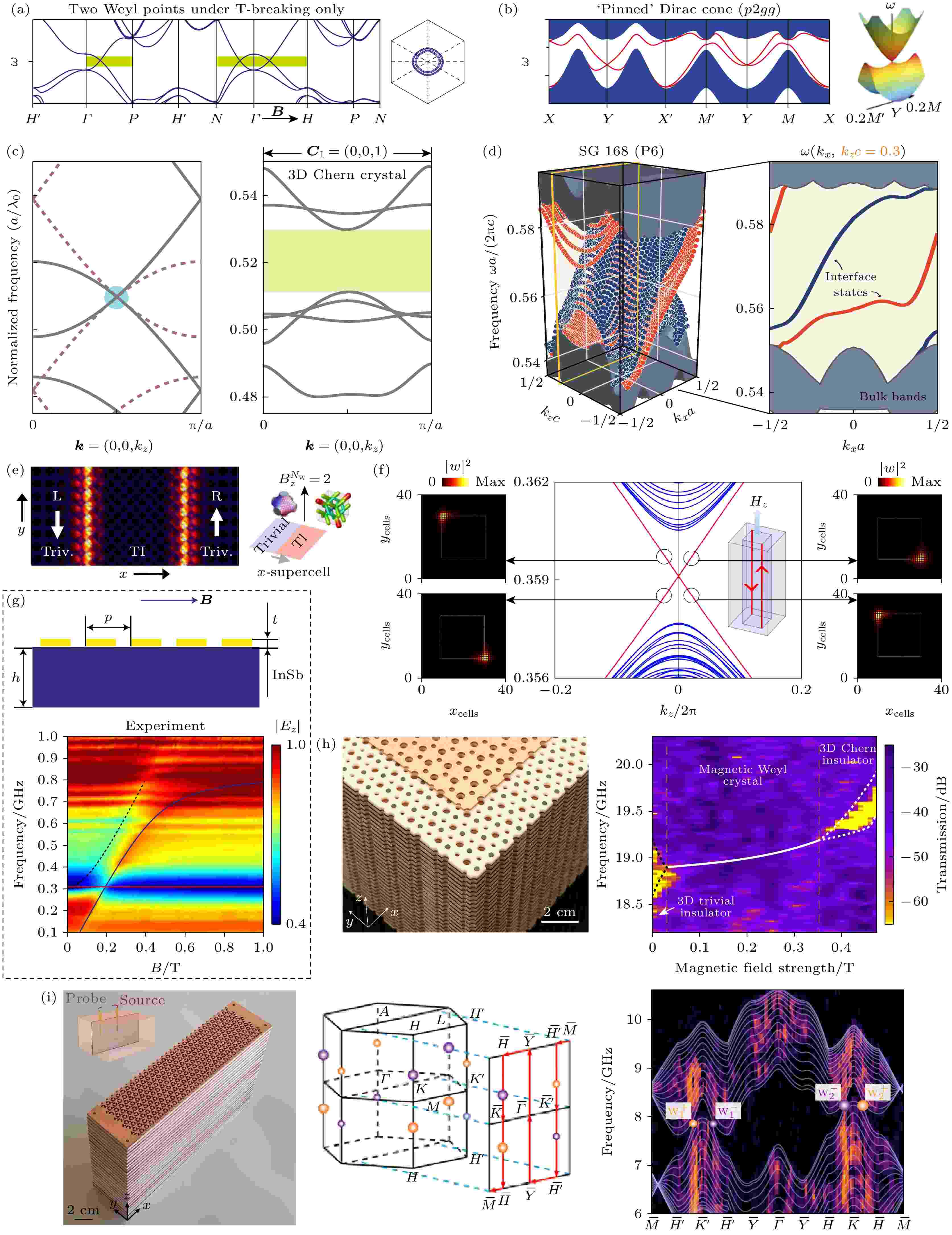
The proposal and development of topological photonics have provided a new approach to fundamentally addressing the susceptibility of traditional photonic devices to defects or disorders, significantly enhancing the transmission efficiency and robustness of photonic devices. Among them, non-reciprocal topological photonics which break time-reversal symmetry and support chiral topological states are crucial branches of topological photonics. Their topological properties are characterized by non-zero Chern numbers in two dimensions or topological Chern vectors in three dimensions, exhibiting a rigorous and complete topological protection beyond that of reciprocal topological photonics. This review focuses on introducing the remarkable achievements of non-reciprocal topological photonics in exploring novel physical phenomena (chiral/antichiral edge/surface states, two-dimensional/three-dimensional photonic Chern insulators, magnetic Weyl photonics crystals, etc.) and constructing non-reciprocal robust topological photonic devices (unidirectional waveguides, broadband slow-light delay lines, arbitrarily shaped topological lasers, high-orbital-angular-momentum coherent light sources, etc.). Finally, the present status, potential challenges, and possible breakthroughs in the development of non-reciprocal topological photonics are discussed.
2024, 73 (7): 076401.
doi: 10.7498/aps.73.20231939
Abstract +
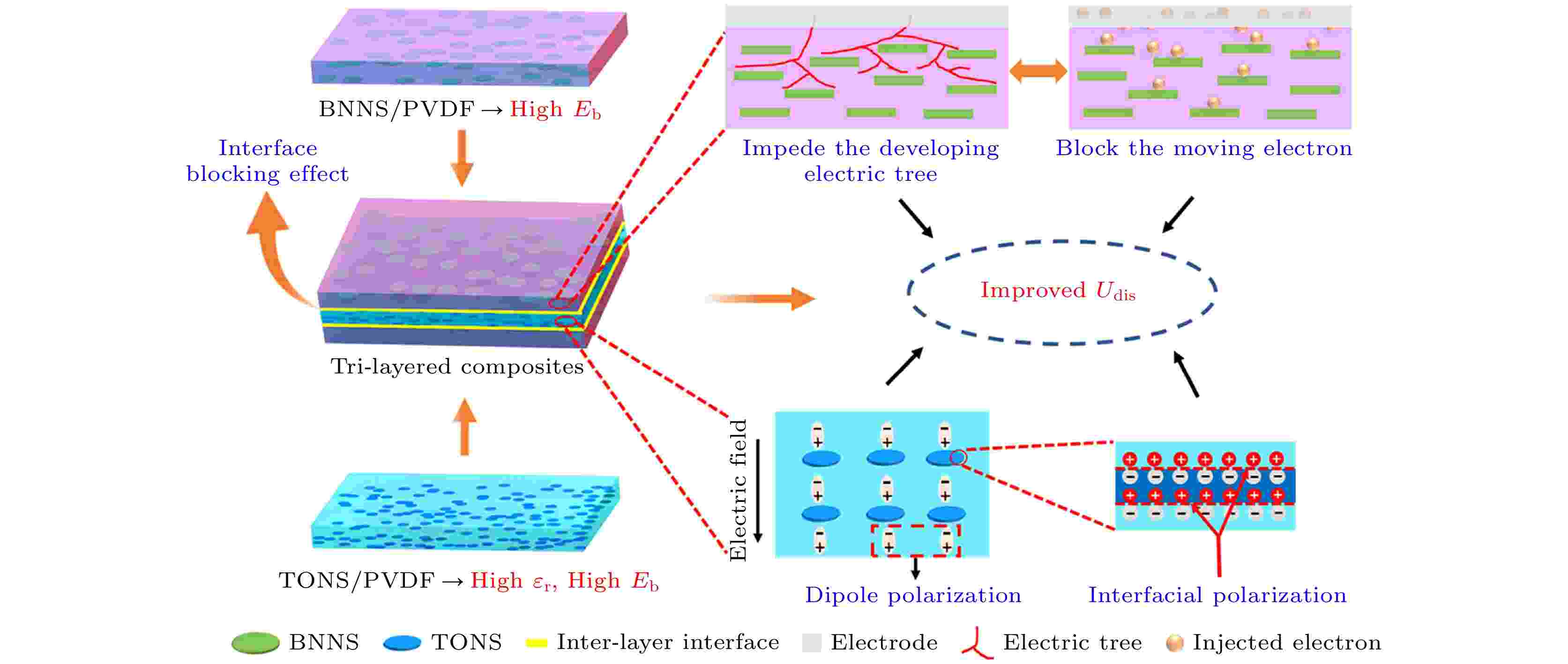
2024, 73 (2): 027702.
doi: 10.7498/aps.73.20230614
Abstract +
2024, 73 (9): 095202.
doi: 10.7498/aps.73.20231625
Abstract +
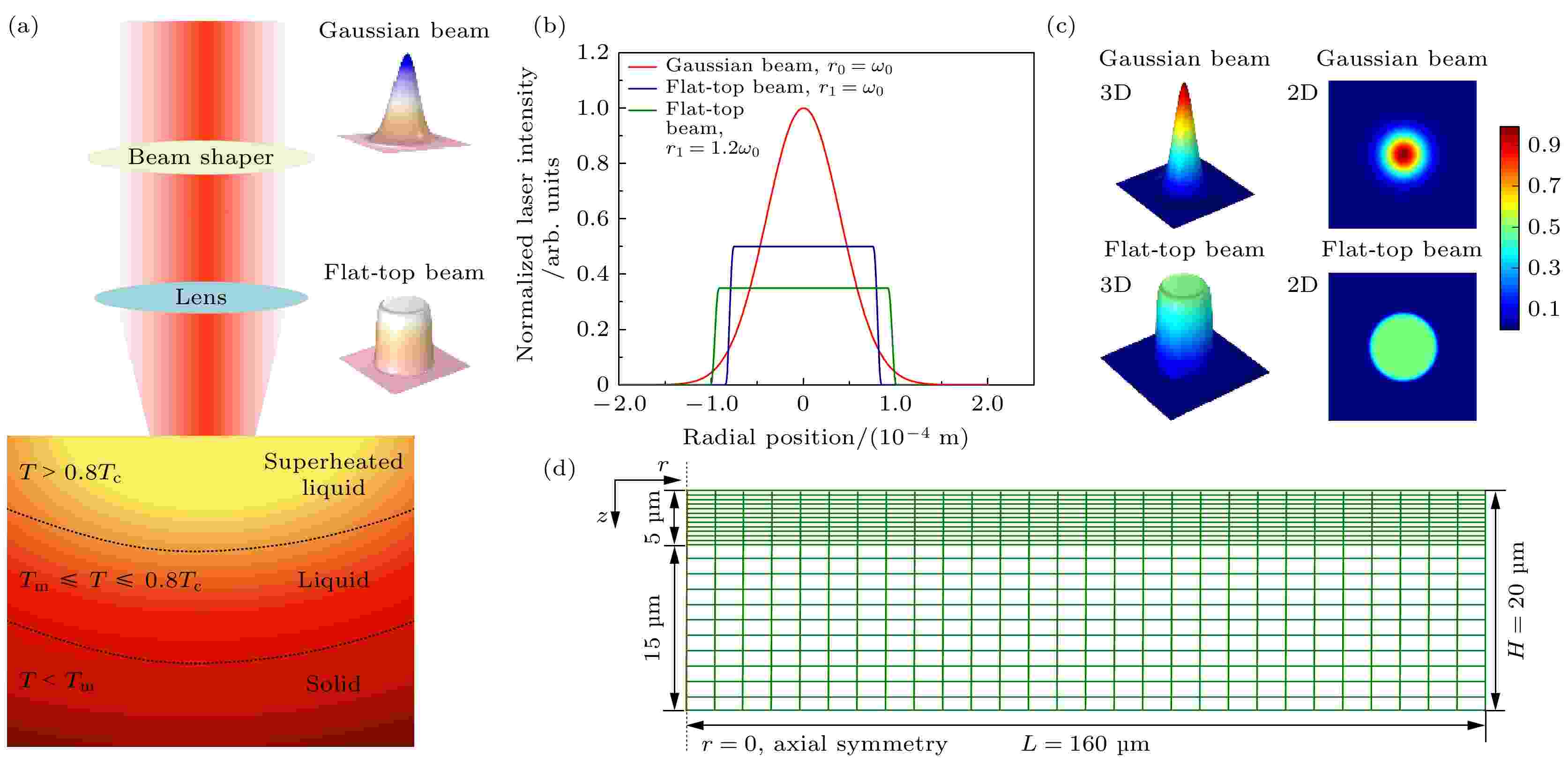
Based on the established two-dimensional asymmetric model of the interaction between a nanosecond pulse laser and metallic aluminum, the effect of beam shaping on the evaporation ablation dynamics during the ablation of metallic aluminum by a nanosecond pulse laser is simulated. The results show that plasma shielding, which has a significant influence on the ablation properties of the target, occurs mainly in the middle phase and late phase of the pulse. Among the three laser profiles, the Gaussian beam has the strongest shielding effect. As the diameter of the reshaped flat-top beam increases, the shielding effect gradually weakens. The two-dimensional spatial distribution of target temperature is relatively different between ablation by a Gaussian beam and that by a flat-top beam. For the Gaussian beam, the center of the target is first heated, and then the temperature spreads in radial direction and axial direction. For the flat-top beam, due to the uniform energy distribution, the target is heated within a certain radial range simultaneously. Beam shaping has a great influence on the evaporation ablation dynamics of the target. For the Gaussian beam, the center of the target is first ablated, followed by the radial ablation. For the flat-top beam, the evaporation time of the target surface is delayed due to the lower energy density after the beam has been shaped. In addition, the target evaporates simultaneously in a certain radial range due to the more uniform distribution of laser energy. For each of the three laser profiles, the evaporation morphology of the target resembles the intensity distribution of the laser beam. The crater produced by the Gaussian beam is deep in the center and shallow on both sides, while it becomes relatively flat by the flat-top beam.
2024, 73 (22): 226401.
doi: 10.7498/aps.73.20240937
Abstract +
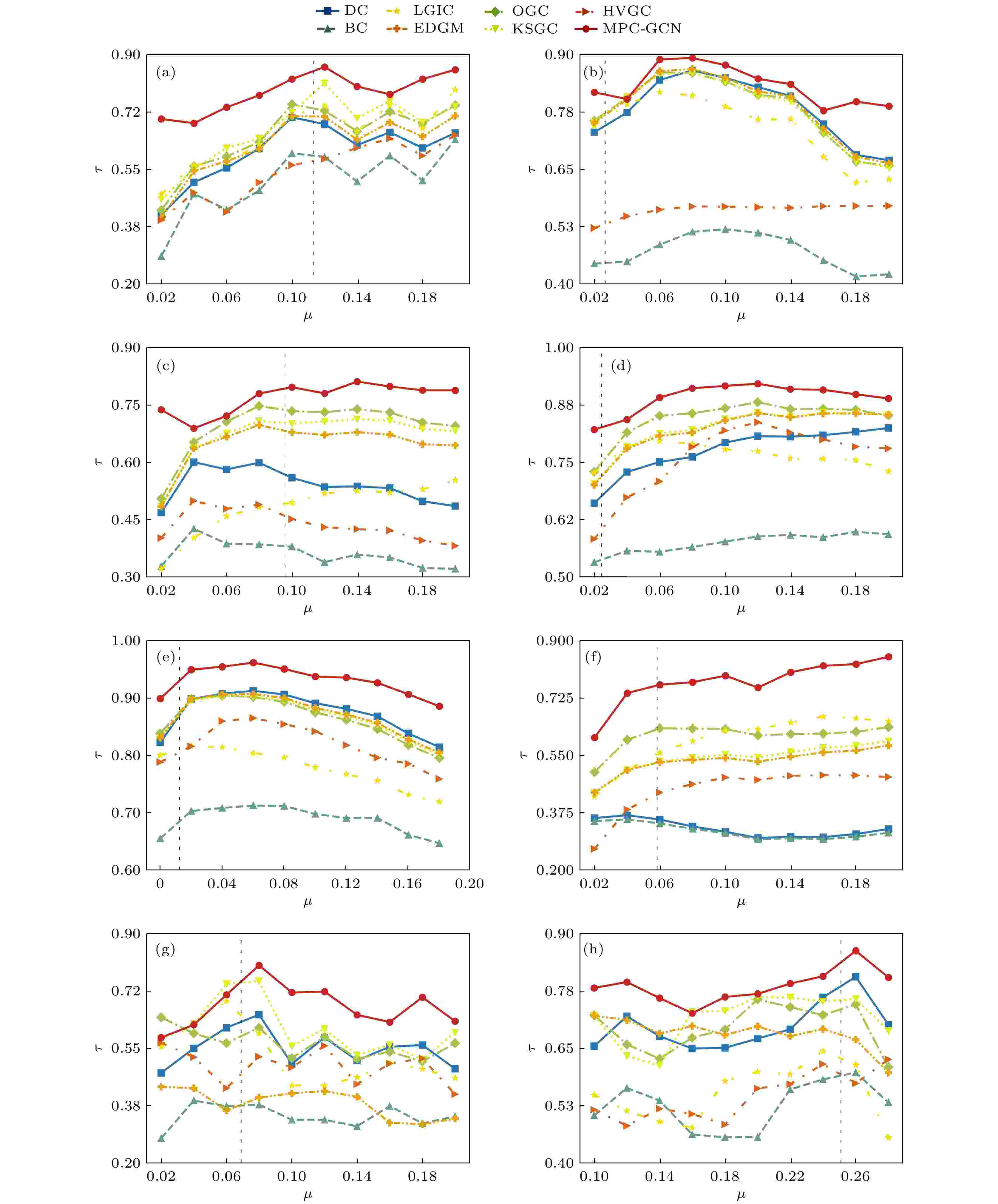
This paper deals with the problem of identifying, evaluating, and ranking key nodes in complex networks by introducing a novel multi-parameter control graph convolutional network (MPC-GCN) for assessing node importance. Drawing inspiration from the multidimensional and hierarchical interactions between nodes in physical systems, this method integrates the automatic feature learning capabilities of graph convolutional networks (GCNs) with a comprehensive analysis of intrinsic properties of nodes, their interactions with neighbors, and their roles in the broader network. The MPC-GCN model provides an innovative framework for identifying key node by using GCNs to iteratively aggregate node and neighbor features across layers. This process captures and combines local, global, and positional characteristics, enabling a more nuanced, multidimensional assessment of node importance. Moreover, the model also includes a flexible parameter adjustment mechanism that allows for adjusting the relative weights of different dimensions, thereby adapting the evaluation process to various network structures. To validate the effectiveness of the model, we first test the influence of model parameters on randomly generated small networks. We then conduct extensive simulations on eight large-scale networks by using the susceptible-infected-recovered (SIR) model. Evaluation metrics, including the M(R) score, Kendall’s tau correlation, the proportion of infected nodes, and the relative size of the largest connected component, are used to assess the model’s performance. The results demonstrate that MPC-GCN outperforms existing methods in terms of monotonicity, accuracy, applicability, and robustness, providing more precise differentiation of node importance. By addressing the limitations of current methods, such as their reliance on single-dimensional perspectives and lack of adaptability, the MPC-GCN provides a more comprehensive and flexible approach to node importance assessment. This method significantly improves the breadth and applicability of node ranking in complex networks.

2024, 73 (12): 128901.
doi: 10.7498/aps.73.20240270
Abstract +
Complex networks serve as indispensable instruments for characterizing and understanding intricate real-world systems. Recently, researchers have delved into the realm of higher-order networks, seeking to delineate interactions within these networks with greater precision or analyze traditional pairwise networks from a higher-dimensional perspective. This effort has unearthed some new phenomena different from those observed in the traditional pairwise networks. However, despite the importance of higher-order networks, research in this area is still in its infancy. In addition, the complexity of higher-order interactions and the lack of standardized definitions for structure-based statistical indicators, also pose challenges to the investigation of higher-order networks. In recognition of these challenges, this paper presents a comprehensive survey of commonly employed statistics and their underlying physical significance in two prevalent types of higher-order networks: hypergraphs and simplicial complex networks. This paper not only outlines the specific calculation methods and application scenarios of these statistical indicators, but also provides a glimpse into future research trends. This comprehensive overview serves as a valuable resource for beginners or cross-disciplinary researchers interested in higher-order networks, enabling them to swiftly grasp the fundamental statistics pertaining to these advanced structures. By promoting a deeper understanding of higher-order networks, this paper facilitates quantitative analysis of their structural characteristics and provides guidance for researchers who aim to develop new statistical methods for higher-order networks.

2024, 73 (3): 038102.
doi: 10.7498/aps.73.20230832
Abstract +
Group III nitride semiconductors, such as GaN, AlN, and InN, are an important class of compound semiconductor material, and have attracted much attention, because of their unique physicochemical properties. These semiconductors possess excellent characteristics, such as wide direct bandgap, high breakdown field strength, high electron mobility, and good stability, and thus are called third-generation semiconductors. Their alloy materials can adjust their bandgaps by changing the type or proportion of group III elements, covering a wide wavelength range from near-ultraviolet to infrared, thereby achieving wavelength selectivity in optoelectronic devices. Atomic layer deposition (ALD) is a unique technique that produces high-quality group III nitride films at low temperatures. The ALD has become an important method of preparing group III nitrides and their alloys. The alloy composition can be easily controlled by adjusting the ALD cycle ratio. This review highlights recent work on the growth and application of group III nitride semiconductors and their alloys by using ALD. The work is summarized according to similarities so as to make it easier to understand the progress and focus of related research. Firstly, this review summarizes binary nitrides with a focus on their mechanism and application. In the section on mechanism investigation, the review categorizes and summarizes the effects of ALD precursor material, substrate, temperature, ALD type, and other conditions on film quality. This demonstrates the effects of different conditions on film growth behavior and quality. The section on application exploration primarily introduces the use of group III nitride films in various devices through ALD, analyzes the enhancing effects of group III nitrides on these devices, and explores the underlying mechanisms. Additionally, this section discusses the growth of group III nitride alloys through ALD, summarizing different deposition methods and conditions. Regarding the ALD growth of group III nitride semiconductors, there is more research on the ALD growth of AlN and GaN, and less research on InN and its alloys. Additionally, there is less research on the ALD growth of GaN for applications, as it is still in the exploratory stage, while there is more research on the ALD growth of AlN for applications. Finally, this review points out the prospects and challenges of ALD in preparation of group III nitride semiconductors and their alloys.

2024, 73 (4): 044204.
doi: 10.7498/aps.73.20231384
Abstract +
2024, 73 (2): 027301.
doi: 10.7498/aps.73.20230556
Abstract +
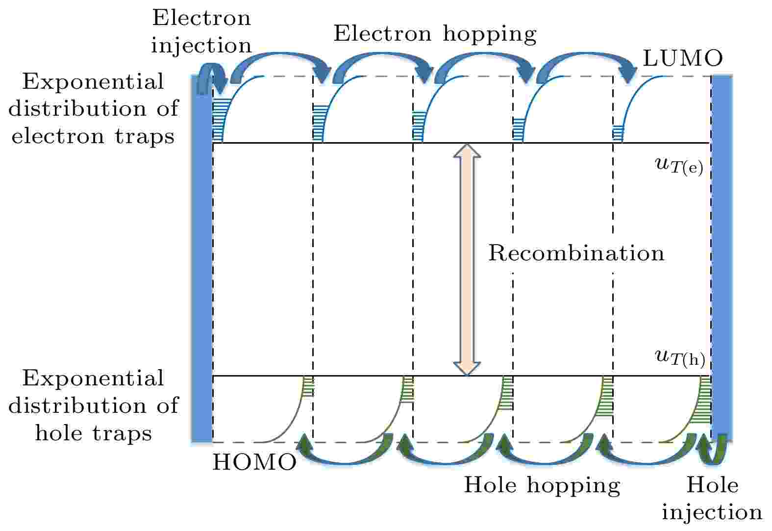
With the development of science and technology, polymer dielectric capacitors are widely used in energy, electronics, transportation, aerospace, and many other areas. For polymer dielectric energy storage capacitors to remain effective in practical applications, excellent charge and discharge performance is essential. However, the performance of the common polymer dielectric capacitors will deteriorate rapidly at high temperature, which makes them fail to work efficiently under worse working conditions. Dielectric trap energy levels and trap densities increase when nanoparticles are incorporated into the dielectric. The change in trap parameters will affect carrier transport. Therefore, the high temperature energy storage performance of polymer nanocomposite dielectric can be improved by changing the trap parameters to regulate the carrier transport process. However, the quantitative relationship between trap energy level and trap density and the energy storage properties of nanocomposite dielectric need further studying. In this paper, the energy storage and release model for exponentially distributed trapped charge jump transport in linear polymer nanocomposite dielectrics is constructed and simulated. The volume resistivity and electric displacement-electric field loops of pure polyetherimide are simulated at 150 ℃, and the simulation results match the experimental results, which demonstrates the validity of the model. Following that, under different temperatures and electric fields, the current density, electric displacement-electric field loops, discharge energy density and charge-discharge efficiency of polyetherimide nanocomposite dielectric are simulated by using different trap parameters. The results show that increasing the maximum trap energy level and the total trap density can effectively reduce the carrier mobility, current density and conductivity loss, and enhance the discharge energy density and the charge-discharge efficiency of the nanocomposite dielectric. On condition that temperature is 150 ℃ and applied electric field is 550 kV/mm, the polyetherimide nanocomposite dielectric with a maximum trap energy level of 1.0 eV and a total trap density of 1×1027 m–3, has 4.26 J·cm–3 of discharge energy density and 98.93% of energy efficiency. Compared with pure polyetherimide, the rate of improvement is 91.09% and 227.58%, respectively. The energy storage performance under high temperature and high electric field is obviously improved. It provides theoretical and model support for the research and development of capacitors with high temperature resistance and energy storage performance.

2024, 73 (23): 230201.
doi: 10.7498/aps.73.20241278
Abstract +
Discovering compact, stable, and easily controllable nanoscale non-trivial topological magnetic structures, such as magnetic skyrmions, is the key to developing next-generation high-density, high-speed, and low-energy non-volatile information storage devices. Based on the topological generation mechanism, magnetic skyrmions can be generated through the Dzyaloshinskii–Moriya interaction (DMI) caused by breaking space-reversal symmetry. Two-dimensional (2D) non-centrosymmetric Janus structurecan generate vertical built-in electric fields to break spatial inversion symmetry. Therefore, seeking for 2D Janus material with intrinsic magnetism is fundamental to develop the novel chiral magnetic storage technologies. In this work, we combine detailed machine learning techniques and first-principle calculations to investigate the magnetism of the unexplored 2D Janus material. We first collect 1179 2D hexagonal ABC-type Janus materials based on the Materials Project database, and use elemental composition as feature descriptors to construct four machine learning models: random forest (RF), gradient boosting decision trees (GBDT), extreme gradient boosting (XGB), and extra trees (ET). These algorithms and models are constructed to predict lattice constants, formation energy, and magnetic moment, via hyperparameter optimization and ten-fold cross-validation. The GBDT exhibits the highest accuracy and best prediction performance for magnetic moment classification. Subsequently, the collected data of 82018 yet-undiscovered 2D Janus materials, are input into the trained models to generate 4024 high magnetic moment 2D Janus materials with thermal stability. First-principles calculations are employed to validate random sample of 13 Janus materials with high magnetic moment. This study provides an effective machine learning framework for classifying the magnetic moments and screening highthroughput 2D Janus structures, thereby accelerating the exploration of their magnetic properties. The datasets provided in this work are available from https://doi.org/10.57760/sciencedb.j00213.00072 .
2024, 73 (7): 070701.
doi: 10.7498/aps.73.20231869
Abstract +
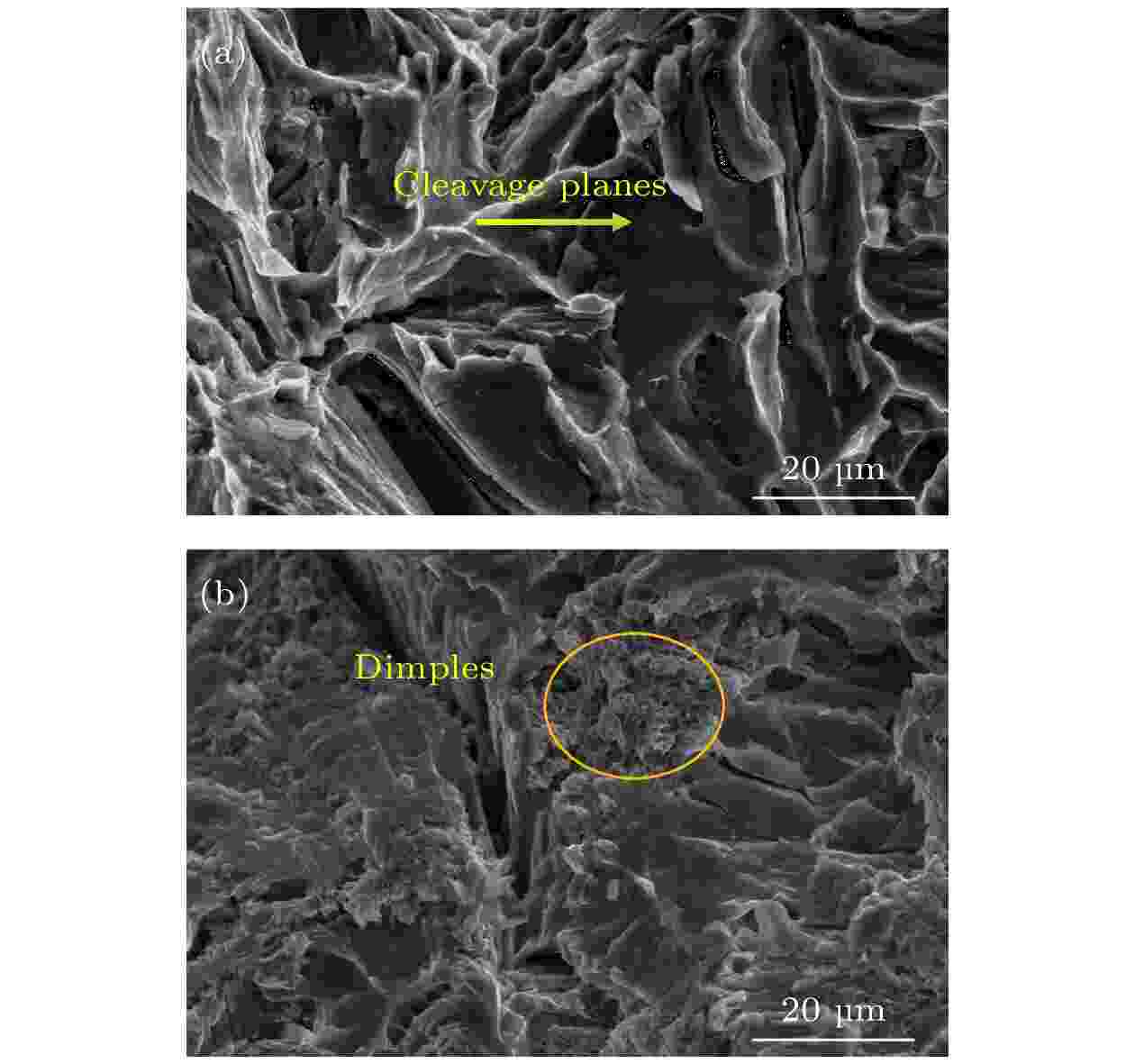
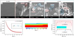
During the long-term operation of a cable, the electrical field, high temperature, and interface stress may age or deteriorate the silicon rubber (SIR) insulation of the cable accessories, affecting the combined electrical-thermal-force performance of the accessories, and easily causing discharge faults. In this work, the electrical-thermal-force properties of silicone rubber for cable accessories under thermal aging and combined force-thermal aging are studied experimentally and numerically. The changes and mechanisms of physical and chemical properties, electrical properties, thermal properties and mechanical properties of silicone rubber are tested and compared before and after aging. The changes of electric, thermal and force field of cable accessories, caused by the change of SIR material parameters under different aging time and aging form, are further simulated. The experimental results show that the crosslinking degree and molecular motion system of SIR will change with the deepening of the aging degree, which will change the electrical-thermal-force properties of the material to different degree. After aging, large agglomeration protrudes and small cavities appear in SIR section, and the damage is more serious under force-thermal aging. The relative dielectric constant first decreases and then increases with the aging time increasing. The volume resistivity, breakdown strength and flashover voltage all first increase and then decrease. The thermal conductivity first increases and then decreases with aging time increasing. In addition, with the increase of aging time, the tensile strength and elongation at break decrease gradually. Considering the change of properties after aging, the destruction of SIR material by force-thermal aging is more serious. The simulation results show that under the two aging modes, the maximum electric field strength at the stress cone root of the cable accessories first increases and then decreases with the increase of time. The electric field strength at the stress cone root of the cable accessories, caused by the force-thermal aging, changes little, maintaining about 2.2 kV/mm. The difference in temperature between the inside and the outside of the insulation layer is obvious under different aging degree, and the temperature difference shows a first decreasing and then increasing trend under both aging modes, and the maximum temperature gradient is 9.15 ℃. The interface stress at the stress cone root decreases from 0.263 to 0.230 MPa, which is about 12.5% lower. This work has guiding significance in evaluating the insulation performance and analyzing the fault of distribution cable accessories.

2024, 73 (7): 074204.
doi: 10.7498/aps.73.20231691
Abstract +
The micro-Doppler effect is a physical phenomenon generated by the micro-motion of objects and their components, which have a significant influence on improving radar detection and resolution capability and also enhancing the radar imaging and target recognition performance. The extraction of micro-Doppler frequency, as a commonly used time-frequency analysis tool, is of great significance in extracting and reconstructing the signal with micro-motion targets. The micro-motion characteristics for moving targets can be verified by using simulation through combining the theory of micro-Doppler effect with the frequency domain model of electromagnetic waves. The simulation research on the micro-motion characteristics of a three-dimensional target is conducted by using the finite element method. The influences of environmental conditions such as relative humidity, visibility, and the presence or absence of turbulence on echo intensity and time-frequency relationship are investigated theoretically. The simulation results indicate that parameters such as relative humidity and visibility, which affect the atmospheric attenuation coefficient, can reduce echo intensity and the period of time-frequency curve. By triggering off beam drift in the transmission path, turbulence can lead to “frequency shift deformation” of the time-frequency curve, degrading the extraction of target motion attitude. A motion attitude classification method is proposed in order to study the micro-Doppler effect better. According to whether the frequency shift changes with time, the motion attitude can be divided into frequency shift time-invariant motion and time-variant motion. Frequency shift time-variant motion includes translation, rolling and vibration. Vibration and rolling are motions that periodically change with time, requiring the comparison of instantaneous frequency shifts at any three times within a cycle. Translation is a time-variant motion with irregular frequency shifts over time, which involves studying instantaneous frequency shifts at any three times. Transient frequency shifts should be analyzed and compared at different times for these motions. The frequency shift time-invariant motion is mainly rotation obtained experimental results indicate that the amplitude, plus-minus, and spectral width of frequency shift at different positions are aimed at inverting the target shape, attitude, direction and velocity. Demodulating one-dimensional data obtained from the FFTshift function can obtain the time-frequency-intensity relationship. This multi-parameter analysis method is a multi-dimensional processing method widely used in the fields of radar, sonar, and communication. The above research is conductive to the measurement of target macroscopic shape properties and the extraction of microscopic motion information, which lays the foundation for radar detection and recognition.
2024, 73 (9): 095201.
doi: 10.7498/aps.73.20231598
Abstract +
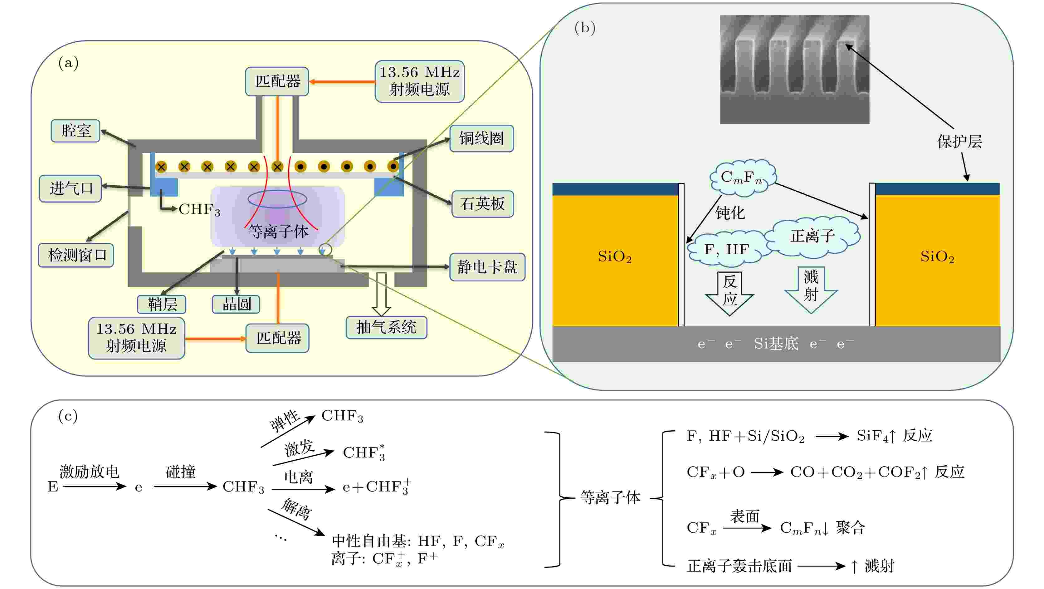
Semiconductor chips are the cornerstone of the information age, which play a vital role in the rapid development of emerging technologies such as big data, machine learning, and artificial intelligence. Driven by the growing demand for computing power, the chip manufacturing industry has been committed to pursuing higher level of integration and smaller device volumes. As a critical step in the chip manufacturing processes, the etching process therefore faces great challenges. Dry etching (or plasma etching) process based on the low-temperature plasma science and technology is the preferred solution for etching the high-precision circuit pattern. In the low-temperature plasma, electrons obtain energy from the external electromagnetic field and transfer the energy to other particles through collision process. After a series of complex physical and chemical reactions, a large number of active particles such as electrons, ions, atoms and molecules in excited states, and radicals are finally generated, providing the material conditions for etching the substrate. Dry etching chamber is a nonlinear system with multiple space-time dimensions, multiple reaction levels and high complexity. Facing such a complex system, only by fully understanding the basic physical and chemical reaction of the etching process can we optimize the process parameters and improve the etching conditions, so as to achieve precision machining of the semiconductor and meet the growing demand of the chip industry for etching rate and yield. In the early days, the process conditions of dry etching were determined through the trial-and-error method, which is characterized by high cost and low yield. However, with the help of plasma simulation, nowadays people have been able to narrow the scope of experiment to a large extent, and find out efficiently the optimal process conditions in a large number of parameters. In this review, we first introduce the basic theory of the mostly used models for plasma simulation including kinetic, fluid dynamic, hybrid and global models, in which the electron collision cross sections are the key input parameters. Since the formation of the low-temperature plasma is driven by the electron-heavy particle collision processes, and the active species for plasma etching are generated in the reactions induced by electron impact, the accuracy and completeness of the cross-section data greatly affect the reliability of the simulation results. Then, the theoretical and experimental methods of obtaining the cross-section data of etching gases are summarized. Finally, the research status of the electron collision cross sections of etching atoms and molecules is summarized, and the future research prospect is discussed.
2024, 73 (5): 054701.
doi: 10.7498/aps.73.20231745
Abstract +
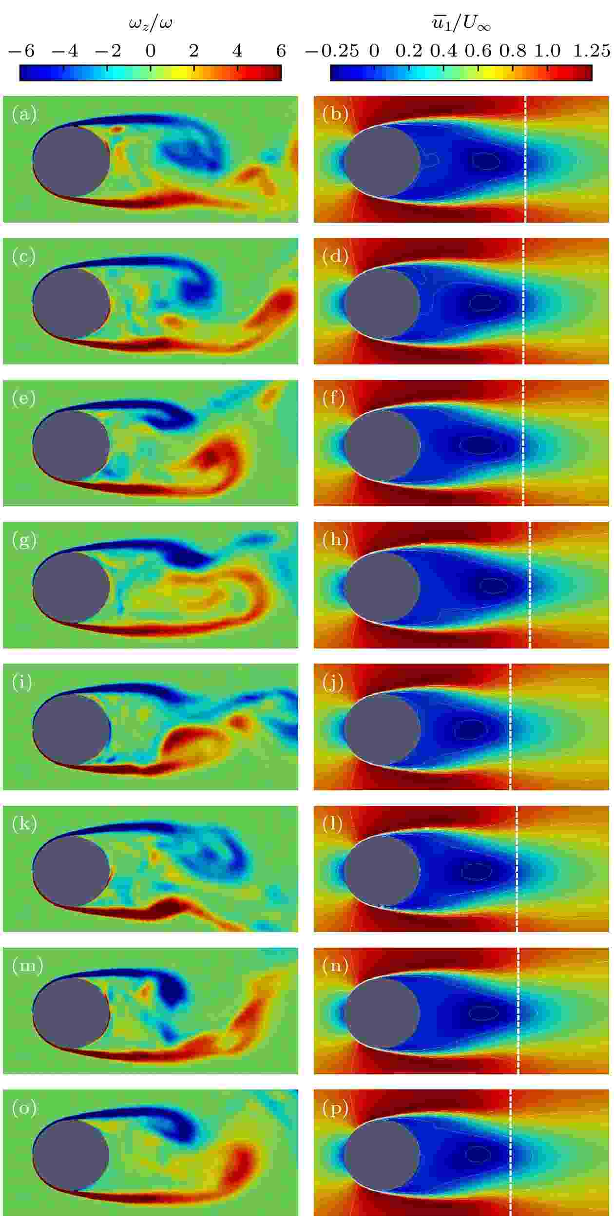
In the present paper, a hybrid RANS/LES model with the wall-modelled LES capability (called WM-HRL model) is developed to perform the high-fidelity CFD simulation investigation for complex flow phenomena around a bluff body with coherent structure in subcritical Reynolds number region. The proposed method can achieve a fast and seamless transition from RANS to LES through a filter parameter rk which is only related to the space resolution capability of the local grid system for various turbulent scales. Furthermore, the boundary positions of the transition region from RANS to LES, as well as the resolving capabilities for the turbulent kinetic energy in the three regions, i.e. RANS, LES and transition region, can be preset by two guide index parameters nrk1-Q and nrk2-Q. Through a series of numerical simulations of the flow around a circular cylinder at Reynolds number Re = 3900, the combination conditions are obtained for such two guide index parameters nrk1-Q and nrk2-Q that have the capability of high-fidelity resolving and capturing temporally- and spatially-developing coherent structures for such complex three-dimensional flows around such a circular cylinder. The results demonstrate that the new WM-HRL model is capable of accurately resolving and capturing the fine spectral structures of the small-scale Kelvin-Helmholtz instability in the shear layer for flow around such a circular cylinder. Furthermore, under a consistent grid system, through different combinations of these two guide index parameters rk1 and rk2, the fine structuresof the recirculation zones with two different lengths and the U-shaped and V-shaped distribution of the average stream-wise velocity in the cylinder near the wake can also be obtained.
2024, 73 (5): 058701.
doi: 10.7498/aps.73.20231569
Abstract +
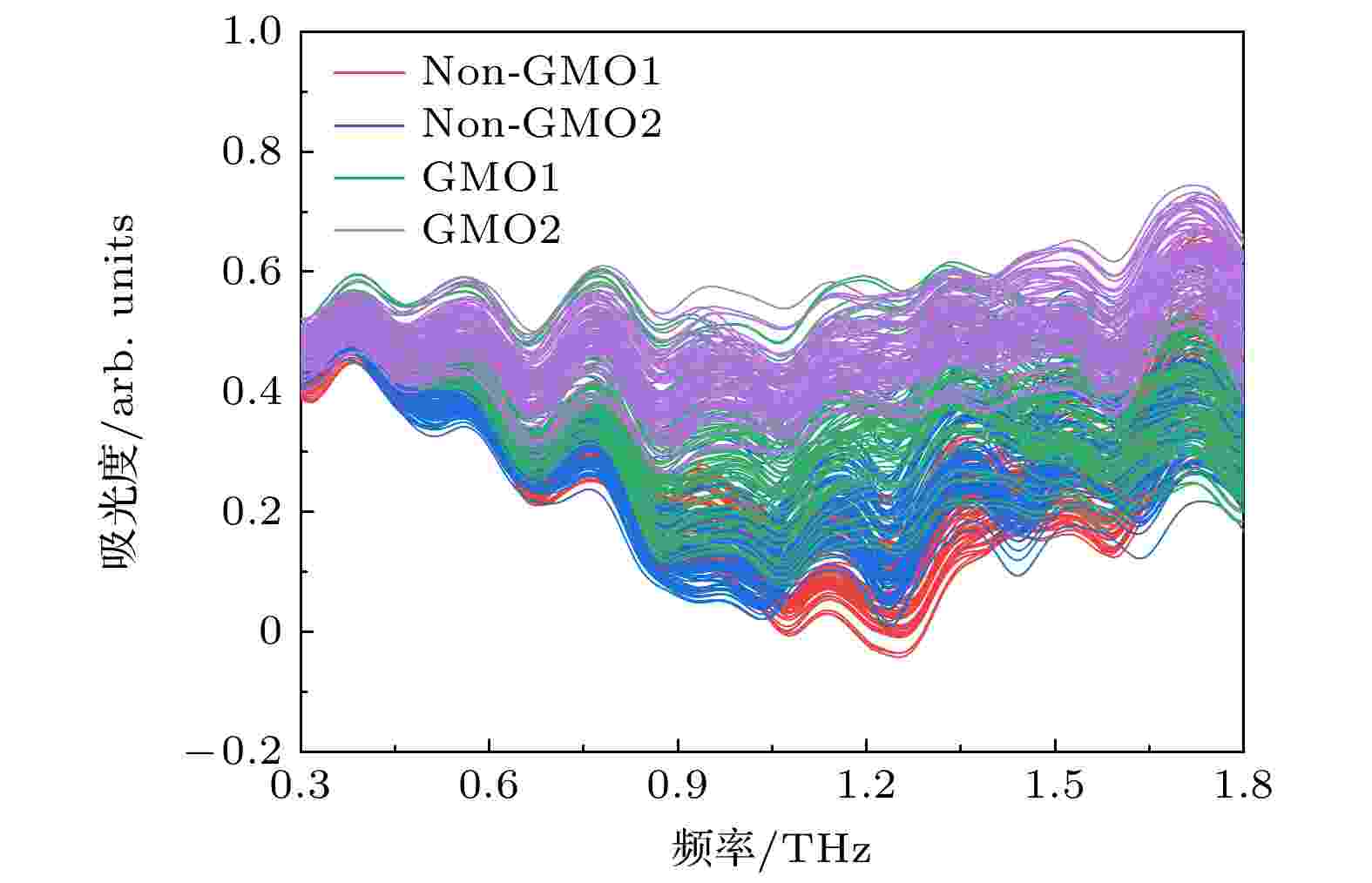
To achieve rapid and accurate identification of genetically modified (GM) and non-GM rapeseed oils, a support vector machine (SVM) model based on an improved mayfly optimization algorithm and coupled with the terahertz time-domain spectroscopy, is proposed. Two types of GM rapeseed oils and two types of non-GM rapeseed oils are selected as research subjects. Their spectral information is acquired by using the terahertz time-domain spectroscopy. The observations show that GM rapeseed oils exhibit stronger terahertz absorption characteristics than non-GM rapeseed oils. However, their absorption spectra are highly similar, making direct differentiation difficult through visual inspection alone. Therefore, SVM is used for spectral recognition. Considering that the classification performance of SVM is significantly affected by its parameters, the mayfly optimization algorithm is combined to optimize these parameters. Furthermore, adaptive inertia weight and Lévy flight strategies are introduced to enhance the global search capability and robustness of the mayfly optimization algorithm, thus addressing the issue of easily becoming trapped in local optima in the optimization process. Moreover, principal component analysis is used to reduce the dimensionality of the absorbance data in a 0.3–1.8 THz range, aiming to extract critical features, thereby enhancing modeling efficiency and reducing redundancy in spectral data. Experimental results demonstrate that the improved mayfly optimization algorithm effectively identifies the optimal parameter combination for SVM, thereby enhancing the overall performance of the identification model. The proposed SVM model, in which the improved mayfly optimization algorithm is used, can achieve a recognition accuracy of 100% for the four types of rapeseed oils, surpassing the 98.15% accuracy achieved by the SVM model with the original mayfly optimization algorithm. Thus, this study presents a rapid and effective new approach for identifying GM rapeseed oils and offers a valuable reference for identifying other genetically modified substances.

- 1
- 2
- 3
- 4
- 5
- ...
- 22
- 23


