


-
单层二硫化钼是制作各种微纳元器件及柔性电子器件较为理想的材料. 然而在实践和应用中, 材料受到环境所导致的应变是一个无法避免的关键问题, 材料的电子结构也会随应变而发生改变. 本文基于第一性原理并结合湿法转移后的拉伸实验, 研究了拉伸应变对单层二硫化钼光电特性的影响. 结果表明: 1)本征单层二硫化钼为直接带隙半导体, 禁带宽度为1.68 eV; 吸收系数曲线最强峰位于10.92 eV附近, 最大吸收系数为1.66 × 105 cm–1. 2)开始施加拉应变(1%)时, 其能带结构从直接带隙转变为间接带隙; 随着应变的增大, 能带仍然保持间接带隙的特征, 且禁带宽度呈现线性下降的趋势; 当拉应变为10%时, 禁带宽度降为0 eV. 吸收系数曲线随应变施加而发生红移. 3)通过对湿法转移后的单层二硫化钼进行拉伸实验, 拉曼光谱中的面内模式
$ {\mathrm{E}}_{2\mathrm{g}}^{1} $ 和面外模式A1g峰都会随拉伸而发生红移, 且两峰的峰值频率差保持在18.6 cm–1左右; 在光致发光谱1.83 eV处观察到单层二硫化钼的A激子的强发射峰. 随着拉应变的变大, 峰值相对强度降低并且线性红移, 代表带隙的线性减小, 与理论计算结果相符.Monolayer molybdenum disulfide is an ideal material for making various micro/nano components and flexible electronic devices. However, the strain of material caused by the environment is a key problem that cannot be avoided in practical applications, and the electronic structure of material will also change with the strain. In this paper, the effect of tensile strain on the photoelectric properties of monolayer MoS2 is studied based on first principles and tensile tests after wet transfer. The results are obtained as follows. 1) Intrinsic monolayer MoS2 is a direct bandgap semiconductor with a band gap of 1.68 eV, the highest peak of the absorption coefficient curve is nearly 10.92 eV, and a maximum absorption coefficient is 1.66 × 105 cm–1. 2) A small tensile strain (1%) will result in the transition from direct to indirect gap for monolayer MoS2. With the increase of strain, the feature of the indirect gap can be preserved but the gap decreases linearly. The gap will decrease to 0 eV when the tensile strain is 10%, and the absorption coefficient curve is red-shifted as a whole with strain. 3) The in-plane mode peak and the out-of-plane mode A1g peak in Raman spectra are re-dshifted with stretching by tensile test of wet-transferred monolayer MoS2, and the difference in peak frequency between the two peaks is maintained at about 18.6 cm–1. The strong emission peak of an exciton of monolayer MoS2 is observed at 1.83 eV of the photoluminescenc spectrum. With the increase of tensile strain, the relative strength of the peak decreases and is linearly re-dshifted, which means that the band gap decreases linearly. It is consistent with the theoretical calculation result.-
Keywords:
- molybdenum disulfide /
- tensile strain /
- energy bands /
- first principles
[1] Lin J, Zhong J, Zhong S, Li H, Zhang H, Chen W 2013 Appl. Phys. Lett. 103 063109
 Google Scholar
[2] Yin Z, Zhang X, Cai Y, Chen J, Wong J I, Tay Y Y 2014 Angew. Chem. Int. Ed. 53 12560
Google Scholar
[3] Que H F, Jiang H N, Wang X G, Zhai P B, Meng L J, Zhang P, Gong Y J 2021 Acta Phys-Chim Sin. 37 2010051
Google Scholar
[4] Kumar S, Sharma A, Tomar M, Gupta V 2021 Mater. Sci. Eng. B 266 11
Google Scholar
[5] Tetsuka H, Nagoya A, Tamura S I 2016 Nanoscale 8 19677
Google Scholar
[6] Singh E, Kim K S, Yeom G Y, Nalwa H S 2017 RSC Advan. 7 28234
Google Scholar
[7] Pak S, Jang A R, Lee J, Hong J, Giraud P, Lee S 2019 Nanoscale 11 4726
Google Scholar
[8] Liu Y, Weiss N O, Duan X D, Cheng H C, Huang Y, Duan X F 2016 Nat. Rev. Mater. 1 17
Google Scholar
[9] Wu W, Wang L, Yu R, Liu Y, Wei S H, Hone J 2016 Advan. Mater. 28 8463
Google Scholar
[10] Liu Z, Amani M, Najmaei S, Xu Q, Zou X, Zhou W 2014 Nat. Commun. 5 5246
Google Scholar
[11] Pak S, Lee J, Jang A, Kim S, Park K, Sohn J I, Cha S 2020 Adv. Funct. Mater. 30 2002023
Google Scholar
[12] Conley H J, Wang B, Ziegler J I, Haglund R F, Pantelides S T, Bolotin K I 2013 Nano Lett. 13 3626
Google Scholar
[13] Dadgar A M, Scullion D, Kang K, Esposito D, Yang E H, Herman I P 2018 Chem. Mat. 30 5148
Google Scholar
[14] 李明林, 万亚玲, 胡建玥, 王卫东 2016 物理学报 65 176201
Google Scholar
Li M L, Wan Y L, Hu J Y, Wang W D 2016 Acta Phys. Sin. 65 176201
Google Scholar
[15] Kuc A, Zibouch N E, Heine T 2011 Phys. Rev. B 83 245213
Google Scholar
[16] 吴木生, 徐波, 刘刚, 欧阳楚英 2012 物理学报 61 227102
Google Scholar
Wu M S, Xu B, Liu G, Ouyang C Y 2012 Acta Phys. Sin. 61 227102
Google Scholar
[17] Wu J Y, Cao P Q, Zhang Z S, Ning F L, Zheng S S, He J Y, Zhang Z L 2018 Nano Lett. 18 1543
Google Scholar
[18] Zhang R, Koutsos V, Cheung R 2016 Appl. Phys. Lett. 108 042104
Google Scholar
[19] Hao S, Yang B, Gao Y 2017 Appl. Phys. Lett. 110 153105
Google Scholar
[20] Yang Y, Li X, Wen M, Hacopian E, Chen W, Gong Y, Zhang J, Li B, Zhou W, Ajayan P M, Chen Q, Zhu T, Lou J 2017 Adv. Mater. 29 1604201
Google Scholar
[21] Yun W S, Han S W, Hong S C, Kim I G, Lee J D 2012 Phys. Rev. B 85 033305
Google Scholar
[22] Hu T, Li R, Dong J M 2013 J. Chem. Phys. 139 174702
Google Scholar
[23] 徐波, 潘必才 2008 物理学报 57 6526
Google Scholar
Xu B, Pan B C 2008 Acta Phys. Sin. 57 6526
Google Scholar
[24] Kresse G, Furthmuller J 1996 Phys. Rev. B 54 11169
Google Scholar
[25] Ramakrishna M, Gomathi A, Manna A K 2010 Angew. Chem. Int. Ed. 122 4153
Google Scholar
[26] Kam K K, Parkinson B A 1982 J. Phys. Chem. 86 463
Google Scholar
[27] Gajdos M, Hummer K, Kresse G 2006 Phys. Rev. B 73 045112
Google Scholar
[28] Kadantsev E S, Hawrylak P 2012 Solid State Commun. 152 909
Google Scholar
[29] Wang W D, Yang C G, Bai L W, Li M L, Li W B 2018 Nanomaterials 8 74
Google Scholar
[30] Mak K F, He K, Lee C, Lee G H, Hone J, Heinz T F 2013 Nat. Mater. 12 207
Google Scholar
-
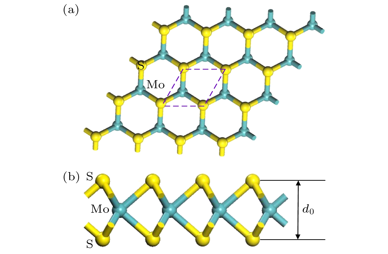
图 1 单层MoS2晶体结构示意图 (a)顶视图; (b)侧视图
Fig. 1. Structure diagram of monolayer MoS2: (a) Top view; (b) side view.
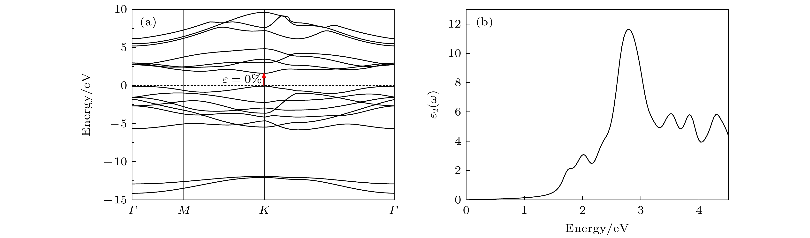
图 3 本征MoS2的(a)能带结构图和(b)介电函数虚部
Fig. 3. (a) Energy band structure of intrinsic MoS2; (b) imaginary part of the intrinsic monolayer MoS2 dielectric function.

图 4 不同拉应变下(1.0%−10%)单层MoS2的能带结构图
Fig. 4. Band structure diagram of monolayer molybdenum disulfide under different tensile strains (1.0%−10%).
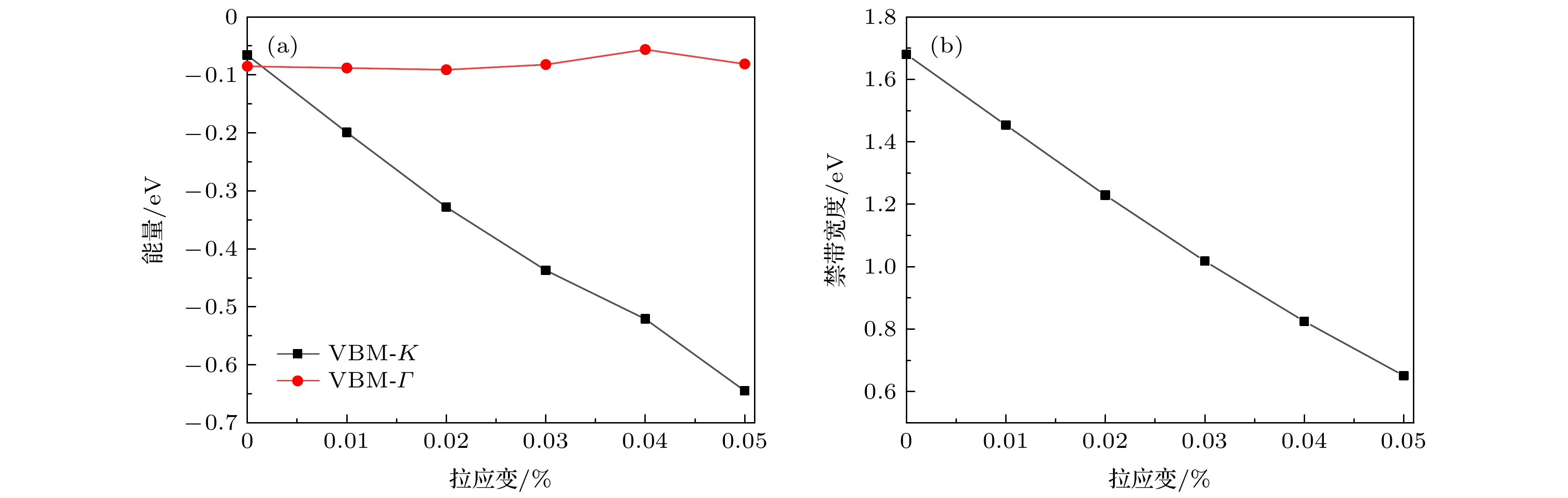
图 5 (a)最高价带(VBM) 上Γ点与K 点的能量随应力增大的变化情况; (b)单层MoS2的禁带宽度随拉应变的变化曲线
Fig. 5. (a) Variation of energy of point Γ and point K on the maximum price band (VBM) with the increase of stress; (b) variation curve of band gap width of monolayer MoS2 with tensile strain.

图 6 单层MoS2在(a)无应变和(b)拉应变5%下的态密度图
Fig. 6. Electron density of states of monolayer MoS2 for (a) zero strain and (b) 5% tensile strain.
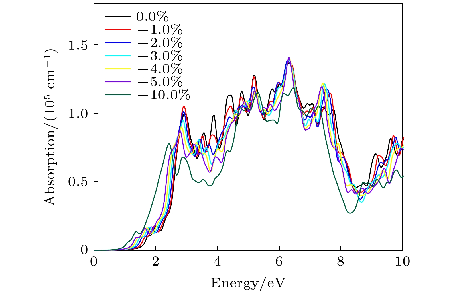
图 7 不同拉应变下的单层MoS2吸收系数图
Fig. 7. Monolayer MoS2 absorption coefficients under different tensile and compressive strains.
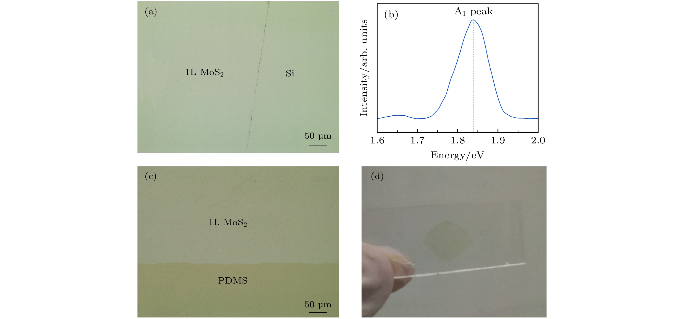
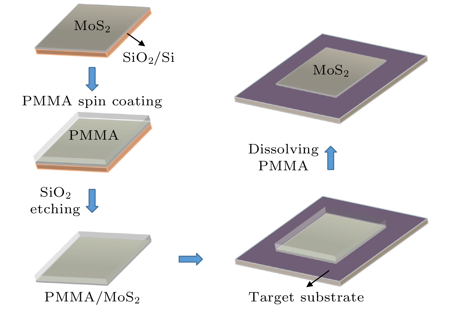
图 8 单层MoS2连续膜通过湿法转移后, (a)转移到Si衬底上的OM图像, (b)转移到Si衬底上的PL光谱, (c)转移到PDMS衬底上的OM图像, (d)转移到PDMS衬底上的实物图
Fig. 8. (a) OM images transferred to Si substrates, (b) PL spectra transferred to Si substrates, (c) OM images transferred to PDMS substrates, (d) real figures transferred to PDMS substrates when monolayer MoS2 continuous film is transferred by wet method.
-
[1] Lin J, Zhong J, Zhong S, Li H, Zhang H, Chen W 2013 Appl. Phys. Lett. 103 063109
Google Scholar
[2] Yin Z, Zhang X, Cai Y, Chen J, Wong J I, Tay Y Y 2014 Angew. Chem. Int. Ed. 53 12560
Google Scholar
[3] Que H F, Jiang H N, Wang X G, Zhai P B, Meng L J, Zhang P, Gong Y J 2021 Acta Phys-Chim Sin. 37 2010051
Google Scholar
[4] Kumar S, Sharma A, Tomar M, Gupta V 2021 Mater. Sci. Eng. B 266 11
Google Scholar
[5] Tetsuka H, Nagoya A, Tamura S I 2016 Nanoscale 8 19677
Google Scholar
[6] Singh E, Kim K S, Yeom G Y, Nalwa H S 2017 RSC Advan. 7 28234
Google Scholar
[7] Pak S, Jang A R, Lee J, Hong J, Giraud P, Lee S 2019 Nanoscale 11 4726
Google Scholar
[8] Liu Y, Weiss N O, Duan X D, Cheng H C, Huang Y, Duan X F 2016 Nat. Rev. Mater. 1 17
Google Scholar
[9] Wu W, Wang L, Yu R, Liu Y, Wei S H, Hone J 2016 Advan. Mater. 28 8463
Google Scholar
[10] Liu Z, Amani M, Najmaei S, Xu Q, Zou X, Zhou W 2014 Nat. Commun. 5 5246
Google Scholar
[11] Pak S, Lee J, Jang A, Kim S, Park K, Sohn J I, Cha S 2020 Adv. Funct. Mater. 30 2002023
Google Scholar
[12] Conley H J, Wang B, Ziegler J I, Haglund R F, Pantelides S T, Bolotin K I 2013 Nano Lett. 13 3626
Google Scholar
[13] Dadgar A M, Scullion D, Kang K, Esposito D, Yang E H, Herman I P 2018 Chem. Mat. 30 5148
Google Scholar
[14] 李明林, 万亚玲, 胡建玥, 王卫东 2016 物理学报 65 176201
Google Scholar
Li M L, Wan Y L, Hu J Y, Wang W D 2016 Acta Phys. Sin. 65 176201
Google Scholar
[15] Kuc A, Zibouch N E, Heine T 2011 Phys. Rev. B 83 245213
Google Scholar
[16] 吴木生, 徐波, 刘刚, 欧阳楚英 2012 物理学报 61 227102
Google Scholar
Wu M S, Xu B, Liu G, Ouyang C Y 2012 Acta Phys. Sin. 61 227102
Google Scholar
[17] Wu J Y, Cao P Q, Zhang Z S, Ning F L, Zheng S S, He J Y, Zhang Z L 2018 Nano Lett. 18 1543
Google Scholar
[18] Zhang R, Koutsos V, Cheung R 2016 Appl. Phys. Lett. 108 042104
Google Scholar
[19] Hao S, Yang B, Gao Y 2017 Appl. Phys. Lett. 110 153105
Google Scholar
[20] Yang Y, Li X, Wen M, Hacopian E, Chen W, Gong Y, Zhang J, Li B, Zhou W, Ajayan P M, Chen Q, Zhu T, Lou J 2017 Adv. Mater. 29 1604201
Google Scholar
[21] Yun W S, Han S W, Hong S C, Kim I G, Lee J D 2012 Phys. Rev. B 85 033305
Google Scholar
[22] Hu T, Li R, Dong J M 2013 J. Chem. Phys. 139 174702
Google Scholar
[23] 徐波, 潘必才 2008 物理学报 57 6526
Google Scholar
Xu B, Pan B C 2008 Acta Phys. Sin. 57 6526
Google Scholar
[24] Kresse G, Furthmuller J 1996 Phys. Rev. B 54 11169
Google Scholar
[25] Ramakrishna M, Gomathi A, Manna A K 2010 Angew. Chem. Int. Ed. 122 4153
Google Scholar
[26] Kam K K, Parkinson B A 1982 J. Phys. Chem. 86 463
Google Scholar
[27] Gajdos M, Hummer K, Kresse G 2006 Phys. Rev. B 73 045112
Google Scholar
[28] Kadantsev E S, Hawrylak P 2012 Solid State Commun. 152 909
Google Scholar
[29] Wang W D, Yang C G, Bai L W, Li M L, Li W B 2018 Nanomaterials 8 74
Google Scholar
[30] Mak K F, He K, Lee C, Lee G H, Hone J, Heinz T F 2013 Nat. Mater. 12 207
Google Scholar


 下载:
下载:

计量
- 文章访问数: 12922
- PDF下载量: 279
- 被引次数: 0
