-
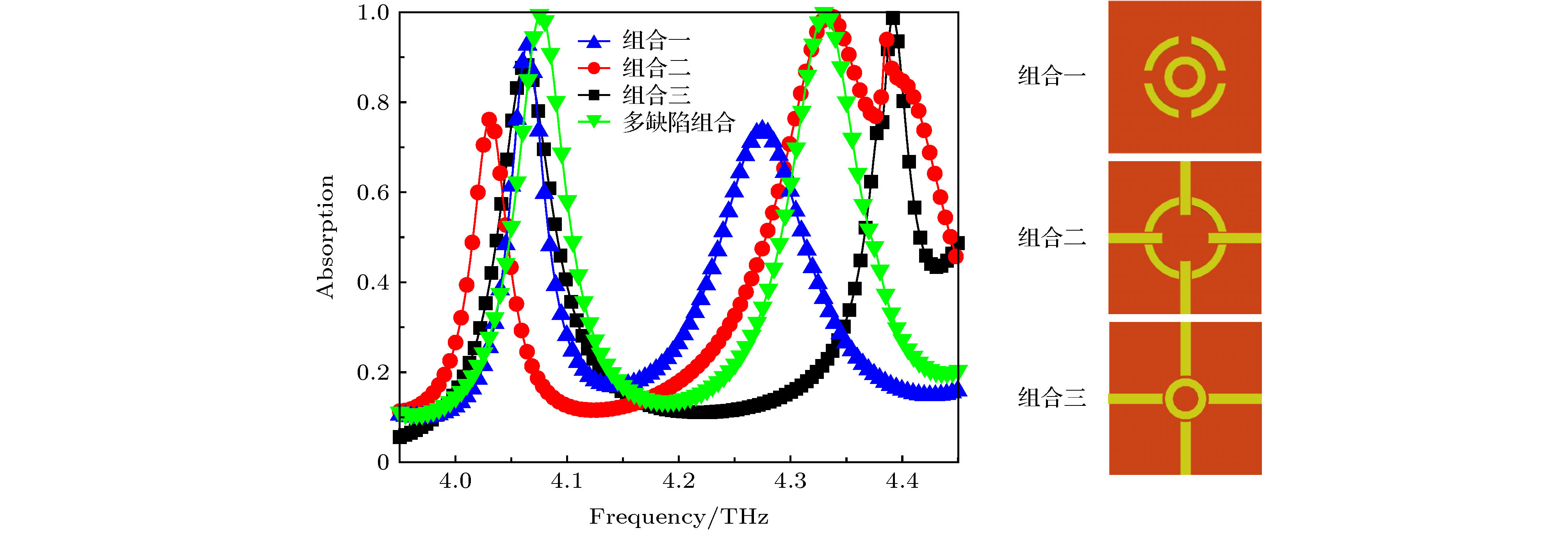
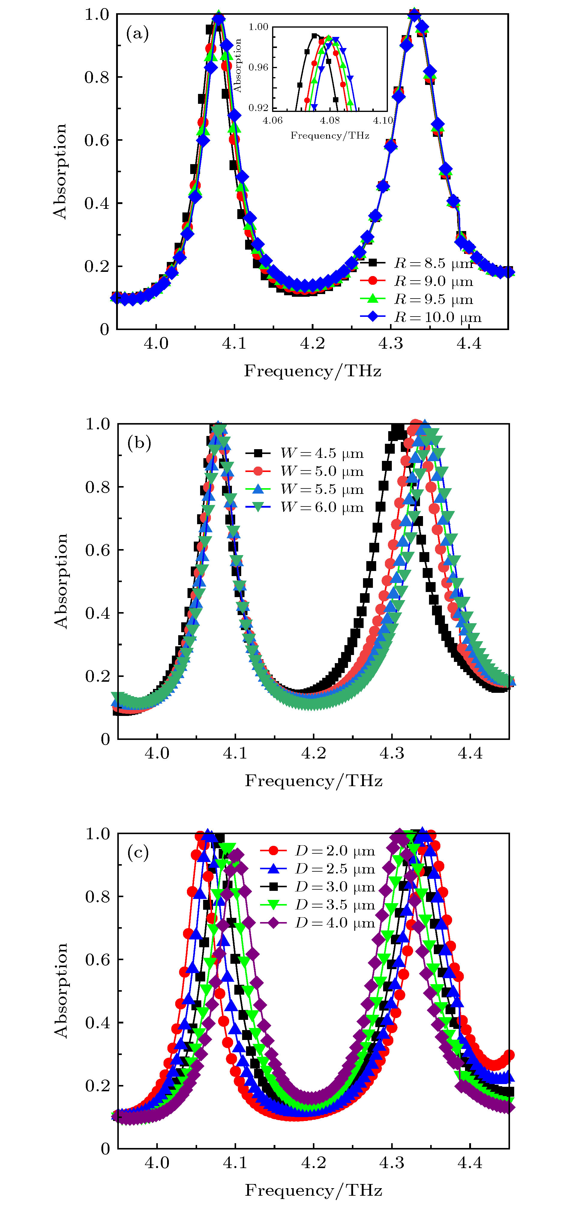
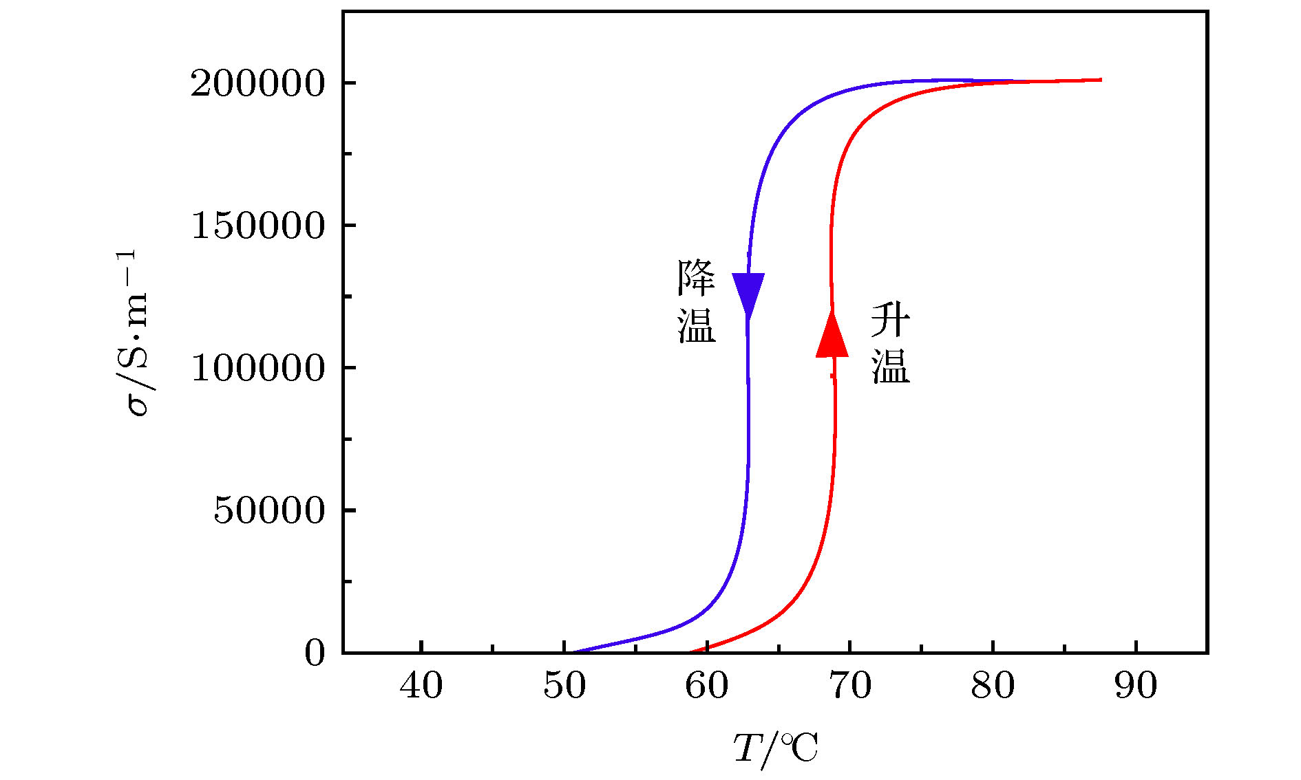
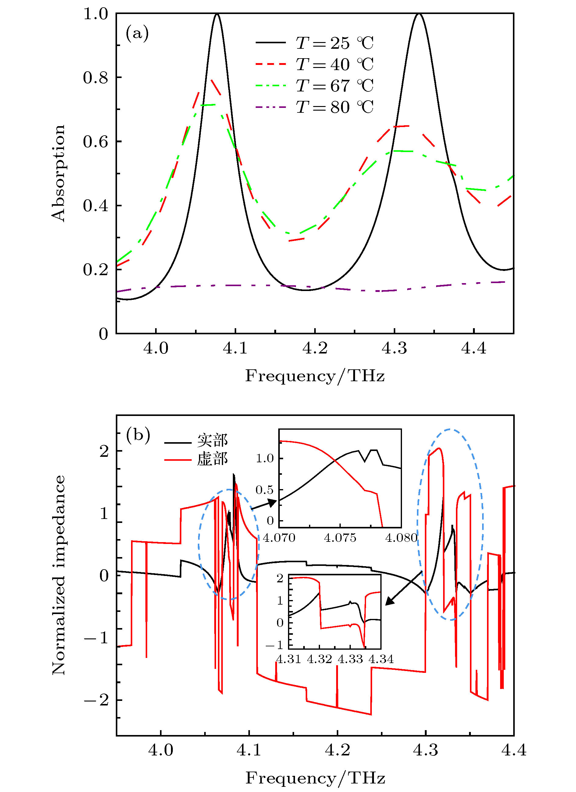
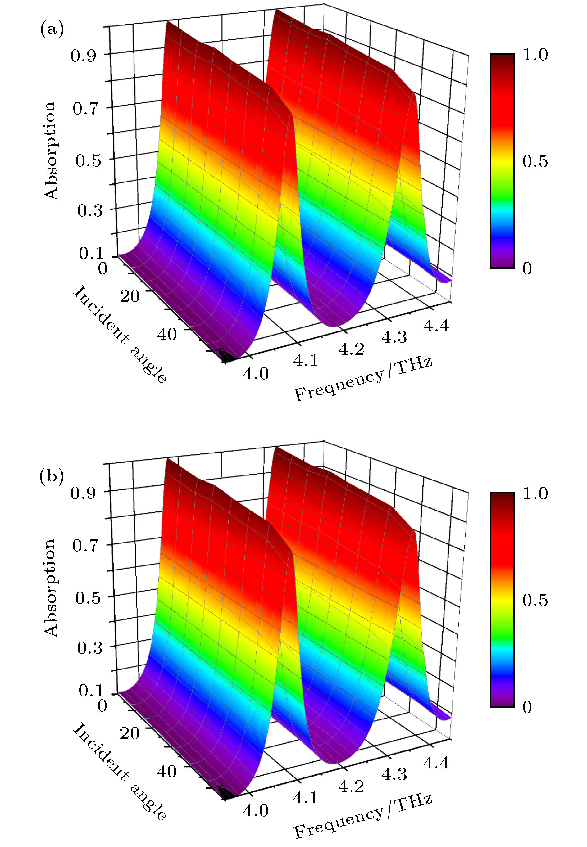
提出一种多缺陷组合嵌入VO2薄膜结构的可调太赫兹吸收器, 它由上表面金属图案层、基体和底层金属板三层结构组成, 在上表面和基体之间嵌入二氧化钒介质. 计算结果表明在f = 4.08 THz和f = 4.33 THz两频点吸收率分别为99.8%和99.9%. 通过改变外界环境温度可控制二氧化钒相变, 从而使两个频点吸收率从99.8%变化到1.0%. 改变入射角和偏振态, 计算结果表明在入射角0°—40°, 吸收器在TE和TM两种极化波下吸收率都能在98%以上. 该太赫兹波吸收器具有高吸收、动态调谐、极化不敏感等特性, 本文所设计的可调太赫兹吸收器在太赫兹波相关领域, 例如探测器、开关、动态调制器、隐身技术等方面具有很好的应用前景.The metamaterial absorber has the advantages of thin thickness, small size, simple structure and high absorption. As is different from the traditional metamaterial absorber, the adjustable material is used for designing the structure, which can realize the dynamic modulation of the device by changing the external factors without changing the device structure. In this paper, an adjustable terahertz absorber with multi-defect combination embedded VO2 thin film is proposed. It is composed of three layers: the upper metal pattern layer, the substrate and the bottom metal plate. Vanadium dioxide medium is sandwiched between the upper surface and the substrate. The absorption performance of the absorber composed of different defect combinations is studied, and the electric field distribution of each combination is analyzed. At the same time, the influences of defects on the absorption performance of the absorber are compared with each other and analyzed. After comprehensive analysis, the defects are combined into the final proposed structure, and the electric field distribution and surface current distribution are analyzed. The relevant parameters affecting the performance of the absorber are scanned and analyzed, and the final optimized structural parameters are obtained. The results show that the absorption rate at f = 4.08 THz and f = 4.33 THz are 99.8% and 99.9%, respectively. The phase transition of vanadium dioxide can be controlled by changing ambient temperature, so that the absorption rates of two frequency points can be changed from 99.8% to 1.0%. In addition, the surface normalized impedance of the proposed absorber is analyzed, which shows that the normalized surface impedance of the designed absorber matches the impedance of the free space well. By changing the incident angle and polarization of terahertz wave, the results show that the absorption rate of the absorber under TE and TM polarization wave both can be more than 98% with the incident angle ranging from 0° to 40°. The proposed terahertz wave absorber has the characteristics of high absorption, dynamic tuning and insensitive polarization. It has good application prospects in terahertz wave related fields such as detectors and stealth technology.
-
Keywords:
- terahertz wave /
- vanadium dioxide /
- multi-defect combination /
- terahertz absorber
[1] Iwaszczuk K, Strikwerda A C, Fan K, Zhang X 2012 Opt. Express. 20 635
 Google Scholar
[2] Tao H, Bingham C M, Strikwerda A C, Pilon D 2008 Phys. Rev. B 78 241103
 Google Scholar
[3] Karaaslan M, Bakır M, Akgol O, Unal E 2017 Opto-Electronics Rev. 25 318
 Google Scholar
[4] Chen C, Sheng Y, Wang J 2017 Opt. Commun. 406 145
 Google Scholar
[5] Landy N I, Bingham C M, Tyler T, Jokerst N M 2009 Phys. Rev. B 79 125104
 Google Scholar
[6] Wan C, Ho Y, Nunez-Sanchez S, Chen L F, Lopez-Garcia M, Pugh J R, Zhu B F, Selvaraj P, Mallick T K, Sundaram S, Cryan J M 2016 Nano. Energy. 26 392
 Google Scholar
[7] Lin K, Chen H, Lai Y, Yu C, Lee Y, Su P, Yen Y T, Chen B 2017 Nano. Energy. 37 61
 Google Scholar
[8] Park J, Kim H J, Nam S H, Kim H, Choi H, Jang Y J, Lee J S, Shin J, Lee H, Baik J M 2016 Nano. Energy. 21 115
 Google Scholar
[9] Lu Y, Dong W, Chen Z, Pors A, Wang Z, Bozhevolnyi S I 2016 Sci. Rep. 6 30650
 Google Scholar
[10] Tan F, Li T, Wang N, Lai S K, Tsoi C C, Yu W, Zhang X 2016 Sci. rep. 6 33049
 Google Scholar
[11] Landy N I, Sajuyigbe S, Mock J J, Smith D R, Padilla W 2008 Phys. Rev. Lett. 100 207402
 Google Scholar
[12] 李爱云, 刘凤收, 王猛, 王岳平, 杨其利 2019 激光杂志 40 28
 Google Scholar
Li A Y, Liu F S, Wang M, Wang Y P, Yang Q L 2019 Laser. J. 40 28
 Google Scholar
[13] Grzeskiewicz B, Sierakowski A, Marczewski J, Pałka N, Wolarz E 2018 Opt-electronics. Rev. 26 329
 Google Scholar
[14] Bakshi S C, Mitra D, Minz L 2018 Plasmonics 13 1843
 Google Scholar
[15] Mohanty A, Acharya O P, Appasani B, Mohapatra S K 2018 Photonic. Nanostruct. 32 74
 Google Scholar
[16] Karimi P, Maddahali M, Bakhtafrouz A, Shahabadi M 2019 IET Optoelectronics 13 5
 Google Scholar
[17] Biabanifard M, Abrishamian M S 2018 Appl. Phys. A 124 826
 Google Scholar
[18] Wang L S, Ding C L, Xia D Y, Ding X Y, Wang Y 2019 IOP Conf. Ser.: Mater. Sci. Eng. 479 012038
 Google Scholar
[19] Daraei O M, Safari M M, Bemani M 2019 eprint ariXiv: 1902.05254
[20] Ding F, Zhong S M, Bozhevolnyi S I 2018 Adv. Opt. Mater. 6 1701204
 Google Scholar
[21] Walther M, Cooke D G, Sherstan C, Hajar M, Freeman M R, Hegmann F A 2007 Phys. Rev. B 76 125408
 Google Scholar
-
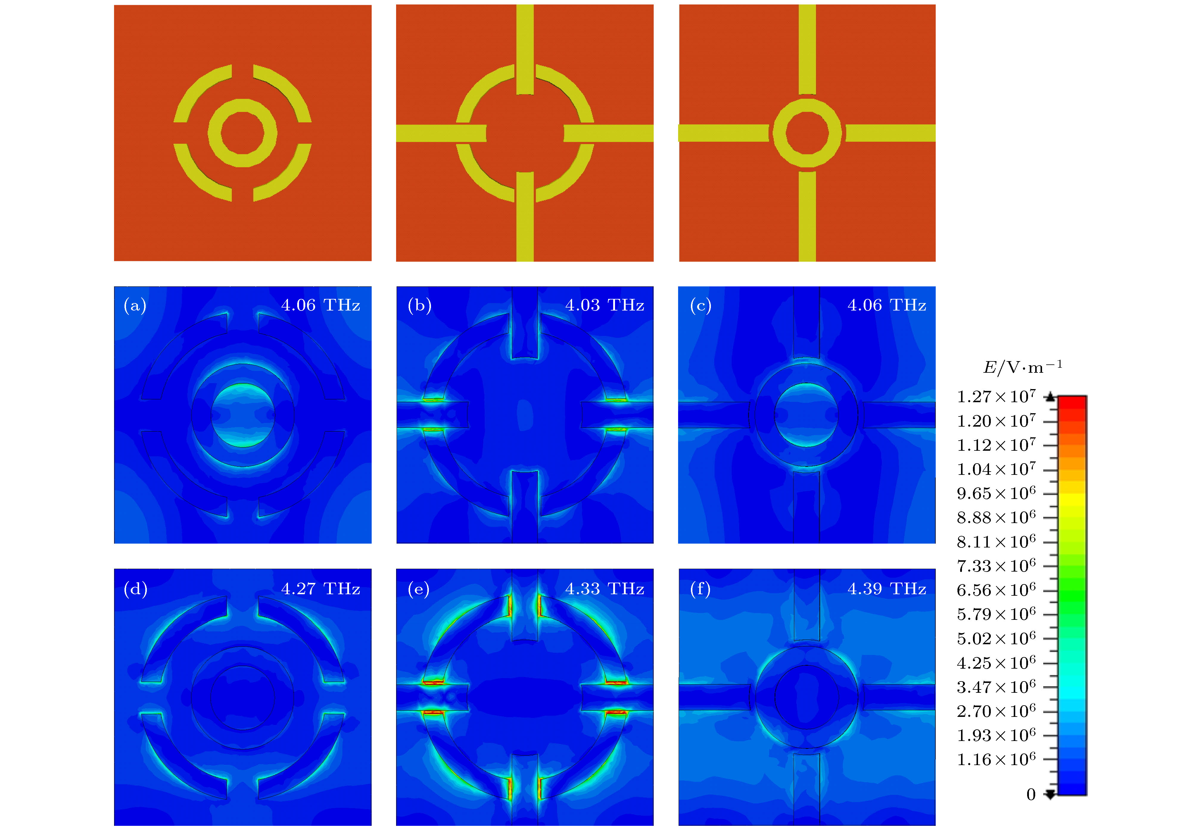
图 3 TE模式下电场E分布图 (a) 组合一, f = 4.06 THz; (d) 组合一, f = 4.27 THz; (b) 组合二, f = 4.03 THz; (e) 组合二, f = 4.33 THz; (c) 组合三, f = 4.06 THz; (f) 组合三, f = 4.39 THz
Fig. 3. Electric field distribution in TE mode: (a) Combination 1, f = 4.06 THz; (d) combination 2, f = 4.27 THz; (b) combination 2, f = 4.03 THz; (e) combination 2, f = 4.33 THz; (c) combination 3, f = 4.06 THz; (f) combination 3, f = 4.39 THz.
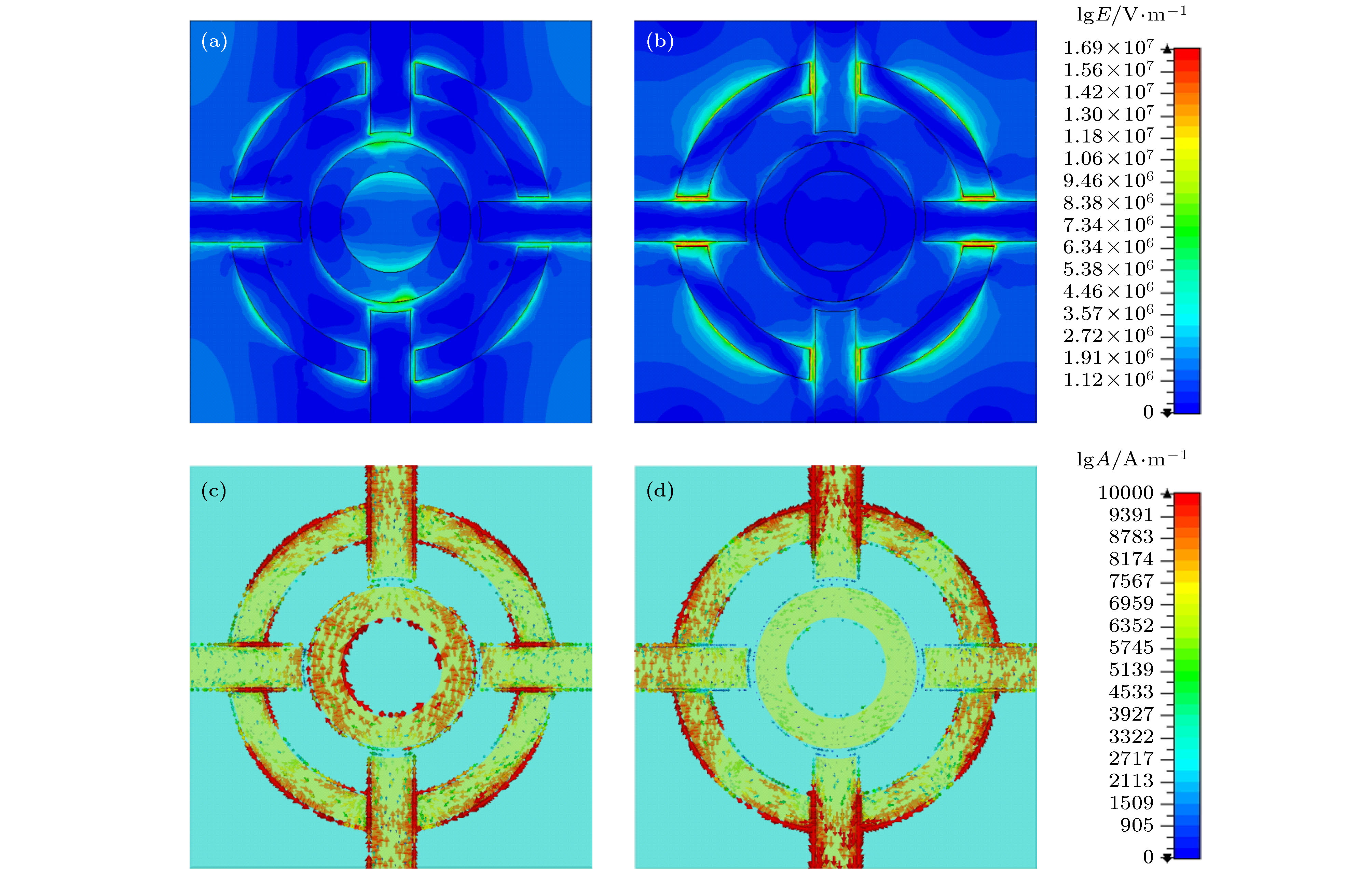
图 4 多缺陷组合TE模式下电场E和电流A分布图 (a) f = 4.08 THz, 电场分布; (b) f = 4.33 THz, 电场分布; (c) f = 4.08 THz, 电流分布; (d) f = 4.33 THz, 电流分布
Fig. 4. Electric field and current distribution in TE mode with multiple defects: (a) f = 4.08 THz, electric field distribution; (b) f = 4.33 THz, electric field distribution; (c) f = 4.08 THz, current distribution; (d) f = 4.33 THz, current distribution.
-
[1] Iwaszczuk K, Strikwerda A C, Fan K, Zhang X 2012 Opt. Express. 20 635
 Google Scholar
[2] Tao H, Bingham C M, Strikwerda A C, Pilon D 2008 Phys. Rev. B 78 241103
 Google Scholar
[3] Karaaslan M, Bakır M, Akgol O, Unal E 2017 Opto-Electronics Rev. 25 318
 Google Scholar
[4] Chen C, Sheng Y, Wang J 2017 Opt. Commun. 406 145
 Google Scholar
[5] Landy N I, Bingham C M, Tyler T, Jokerst N M 2009 Phys. Rev. B 79 125104
 Google Scholar
[6] Wan C, Ho Y, Nunez-Sanchez S, Chen L F, Lopez-Garcia M, Pugh J R, Zhu B F, Selvaraj P, Mallick T K, Sundaram S, Cryan J M 2016 Nano. Energy. 26 392
 Google Scholar
[7] Lin K, Chen H, Lai Y, Yu C, Lee Y, Su P, Yen Y T, Chen B 2017 Nano. Energy. 37 61
 Google Scholar
[8] Park J, Kim H J, Nam S H, Kim H, Choi H, Jang Y J, Lee J S, Shin J, Lee H, Baik J M 2016 Nano. Energy. 21 115
 Google Scholar
[9] Lu Y, Dong W, Chen Z, Pors A, Wang Z, Bozhevolnyi S I 2016 Sci. Rep. 6 30650
 Google Scholar
[10] Tan F, Li T, Wang N, Lai S K, Tsoi C C, Yu W, Zhang X 2016 Sci. rep. 6 33049
 Google Scholar
[11] Landy N I, Sajuyigbe S, Mock J J, Smith D R, Padilla W 2008 Phys. Rev. Lett. 100 207402
 Google Scholar
[12] 李爱云, 刘凤收, 王猛, 王岳平, 杨其利 2019 激光杂志 40 28
 Google Scholar
Li A Y, Liu F S, Wang M, Wang Y P, Yang Q L 2019 Laser. J. 40 28
 Google Scholar
[13] Grzeskiewicz B, Sierakowski A, Marczewski J, Pałka N, Wolarz E 2018 Opt-electronics. Rev. 26 329
 Google Scholar
[14] Bakshi S C, Mitra D, Minz L 2018 Plasmonics 13 1843
 Google Scholar
[15] Mohanty A, Acharya O P, Appasani B, Mohapatra S K 2018 Photonic. Nanostruct. 32 74
 Google Scholar
[16] Karimi P, Maddahali M, Bakhtafrouz A, Shahabadi M 2019 IET Optoelectronics 13 5
 Google Scholar
[17] Biabanifard M, Abrishamian M S 2018 Appl. Phys. A 124 826
 Google Scholar
[18] Wang L S, Ding C L, Xia D Y, Ding X Y, Wang Y 2019 IOP Conf. Ser.: Mater. Sci. Eng. 479 012038
 Google Scholar
[19] Daraei O M, Safari M M, Bemani M 2019 eprint ariXiv: 1902.05254
[20] Ding F, Zhong S M, Bozhevolnyi S I 2018 Adv. Opt. Mater. 6 1701204
 Google Scholar
[21] Walther M, Cooke D G, Sherstan C, Hajar M, Freeman M R, Hegmann F A 2007 Phys. Rev. B 76 125408
 Google Scholar
计量
- 文章访问数: 11514
- PDF下载量: 182
- 被引次数: 0


 下载:
下载:
