


-
自旋转移矩辅助电压调控磁各向异性磁隧道结(STT辅助VCMA-MTJ)作为非易失性全加器(NV-FA)中的核心部件, 具有切换速度快、功耗低, 稳定性好等优点, 将在物联网、人工智能等领域具有良好的发展前景. 然而随着磁隧道结(MTJ)尺寸的不断缩小以及芯片集成度的不断提高, 工艺偏差对MTJ及NV-FA电路性能的影响将变得越来越显著. 本文基于STT辅助VCMA-MTJ磁化动力学, 在充分考虑薄膜生长工艺偏差以及刻蚀工艺偏差影响的情况下, 建立了更为精确的STT辅助VCMA-MTJ电学模型, 研究了上述两种工艺偏差对MTJ及NV-FA电路性能的影响. 结果表明, 当自由层厚度偏差γtf ≥ 6%或氧化层厚度偏差γtox ≥ 0.7%时, MTJ将无法实现状态切换; 当隧穿磁阻率偏差β增大到30%时, 读取裕度SM将下降高达17.6%. 对于NV-FA电路, 通过增大电压Vb1以及写‘0’时增大电压Vb2或写‘1’时减小Vb2, 可有效降低非易失性加数写入错误率; 通过增大逻辑运算驱动电压Vdd, 可有效降低逻辑运算结果输出错误率.As one of the key components in the non-volatile full adder (NV-FA), spin transfer torque assisted voltage controlled magnetic anisotropy magnetic tunnel junction (STT assisted VCMA-MTJ) will possess superior development prospects in internet of things, artificial intelligence and other fields due to its fast switching speed, low power consumption and good stability. However, with the downscaling of magnetic tunnel junction (MTJ) and the improvement of chip integration, the effects of process deviation on the performances of MTJ device as well as NV-FA circuit become more and more important. Based on the magnetization dynamics of STT assisted VCMA-MTJ, a new electrical model of STT assisted VCMA-MTJ, in which the effects of the film growth variation and the etching variation are taken into account, is established to study the effects of the above deviations on the performances of MTJ device and NV-FA circuit. It is shown that the MTJ state fails to be switched under the free layer thickness deviation γtf ≥ 6% or the oxide layer thickness deviation γtox ≥ 0.7%. The sensing margin (SM) is reduced by 17.5% as the tunnel magnetoresistance ratio deviation β increases to 30%. The writing error rate can be effectively reduced by increasing Vb1, and increasing Vb2 when writing ‘0’ or reducing Vb2 when writing ‘1’ in the NV-FA circuit. The output error rate can also be effectively reduced by increasing the driving voltage of logical operation Vdd.
-
Keywords:
- magnetic tunnel junction /
- spin transfer torque /
- voltage controlled magnetic anisotropy magnetic /
- process deviation
[1] Verma G 2020 Global Conference on Wireless and Optical Technologies (GCWOT) Malaga, Spain, October 6–8, 2020 p1
[2] Deng E Y, Zhang Y, Klein J O, Ravelsona D, Chappert C, Zhao W S 2013 IEEE Trans. Magn. 49 4982
 Google Scholar
[3] Cai H, Jiang H L, Han M L, Wang Z H, Wang Y, Yang J, Han J, Liu L B, Zhao W S 2019 IEEE Computer Society Annual Symposium on VLSI (ISVLSI) Miami, USA, July 1, 2019 p111
[4] Shreya S, Jain A, Kaushik B K 2020 Microelectron. J. 109 104943
Google Scholar
[5] Roohi A, Zand R, Fan D, DeMara R F 2017 IEEE Trans. Comput. AD. D. 36 2134
Google Scholar
[6] Sharmin S, Jaiswal A, Roy K 2016 IEEE Trans. Electron. Devices 63 3493
Google Scholar
[7] Wang Y, Cai H, Naviner L, Zhang Y, Zhao X X, Deng E Y, Klein J O, Zhao W S 2016 IEEE Trans. Electron. Devices 63 1762
Google Scholar
[8] Long M Z, Zeng L, Gao T Q, Zhang D M, Qin X W, Zhang Y G, Zhao W S 2018 IEEE Trans. Nanotechnol. 17 492
Google Scholar
[9] Kanai S, Nakatani Y, Yamanouchi M, Ikeda S, Sato H, Matsukura F, Ohno H 2014 Appl. Phys. Lett. 104 212406
Google Scholar
[10] Zarei A, Safaei F 2018 Microelectron. J. 82 62
Google Scholar
[11] Wang Y, Cai H, Naviner L, Zhao X X, Zhang Y, Slimani M, Klein J O, Zhao W S 2016 Microelectron. Reliab. 64 26
Google Scholar
[12] Meng H, Lum W H, Sbiaa R, Lua S Y H, Tan H K 2011 J. Appl. Phys. 110 033904
Google Scholar
[13] Chun S W, Kim D, Kwon J 2012 J. Appl. Phys. 111 07C722
Google Scholar
[14] Jeong J, Endoh T 2017 Jpn. J. Appl. Phys. 56 04CE09
Google Scholar
[15] Ji M H, Pan L, Hu Y G, Pan M C, Yang L, Peng J P, Qiu W C, Hu J F, Zhang Q, Li P S 2019 AIP Adv. 9 085317
Google Scholar
[16] Amiri P K, Alzate J G, Cai X Q, Ebrahimi F, Hu Q, Wong K, Grezes C, Lee H, Yu G Q, Li X, Akyol M, Shao Q M, Katine J A, Langer J, Ocker B, Wang K L 2015 IEEE Trans. Magn. 51 1
Google Scholar
[17] Liu Y W, Zhang Z Z 2013 Sci. China Phys. Mech. 56 184
Google Scholar
[18] Niranjan M K, Duan C G, Jaswal S S, Tsymbal E V 2010 Appl. Phys. Lett. 96 222504
Google Scholar
[19] Zhao W S, Zhao X X, Zhang B Y, Cao K H, Wang L Z, Kang W, Shi Q, Wang M X, Zhang Y, Wang Y, Peng S Z, Klein J O, Naviner L, Ravelosona D 2016 Materals 9 41
Google Scholar
[20] Kang W, Ran Y, Zhang Y G, Lv W F, Zhao W S 2017 IEEE Trans. Nanotechnol. 16 387
Google Scholar
[21] Brinkman W F, Dynes R C, Rowell J M 1970 J. Appl. Phys. 41 1915
Google Scholar
[22] 金冬月, 陈虎, 王佑, 张万荣, 那伟聪, 郭斌, 吴玲, 杨绍萌, 孙晟 2020 物理学报 69 198502
Google Scholar
Jin D Y, Chen H, Wang Y, Zhang W R, Na W C, Guo B, Wu L, Yang S M, Sun S 2020 Acta Phys. Sin. 69 198502
Google Scholar
[23] Gajek M, Nowak J J, Sun J Z, Trouilloud P L, O’Sullivan E J, Abraham D W, Gaidis M C, Hu G, Brown S, Zhu Y, Robertazzi R P, Gallagher W J 2012 Appl. Phys. Lett. 100 132408
Google Scholar
[24] Chen E, Schwarz B, Choi C J, Kula W, Wolfman J, Ounadjela K, Geha S 2003 J. Appl. Phys. 93 8379
Google Scholar
[25] Wu L Z, Taouil M, Rao S, Marinissen E J, Hamdioui S 2018 IEEE International Test Conference (ITC) Phoenix, USA, October 29–November 1, 2018 p18412682
[26] Sugiura K, Takahashi S, Amano M, Kajiyama T, Iwayama M, Asao Y, Shimomura N, Kishi T, Ikegawa S, Yoda H, Nitayama A 2009 Jpn. J. Appl. Phys. 48 08HD02
Google Scholar
[27] Kinoshita K, Utsumi H, Suemitsu K, Hada H, Sugibayashi T 2010 Jpn. J. Appl. Phys. 49 08JB02
Google Scholar
[28] Kinoshita K, Yamamoto T, Honjo H, Kasai N, Ikeda S, Ohno H 2012 Jpn. J. Appl. Phys. 51 08HA01
Google Scholar
[29] Deng E Y, Wang Y, Wang Z H, Klein J O, Dieny B, Prenat G, Zhao W S 2015 Proceedings of the 2015 IEEE/ACM International Symposium on Nanoscale Architectures Boston, USA, July 8–10, 2015 p27
[30] Li J, Augustine C, Salahuddin S, Roy K 2008 Proceedings of the 45th annual Design Automation Conference New York, USA, June 8–13, 2008 p278
[31] Cai H, Wang Y, Naviner L, Zhao W S 2017 IEEE T. Circuits-I 64 847
Google Scholar
-
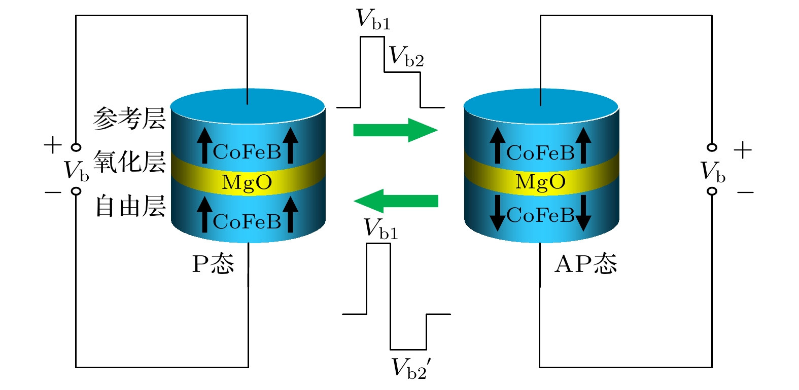
图 1 STT辅助VCMA-MTJ结构示意图
Fig. 1. Schematic structure of the STT assisted VCMA-MTJ device.
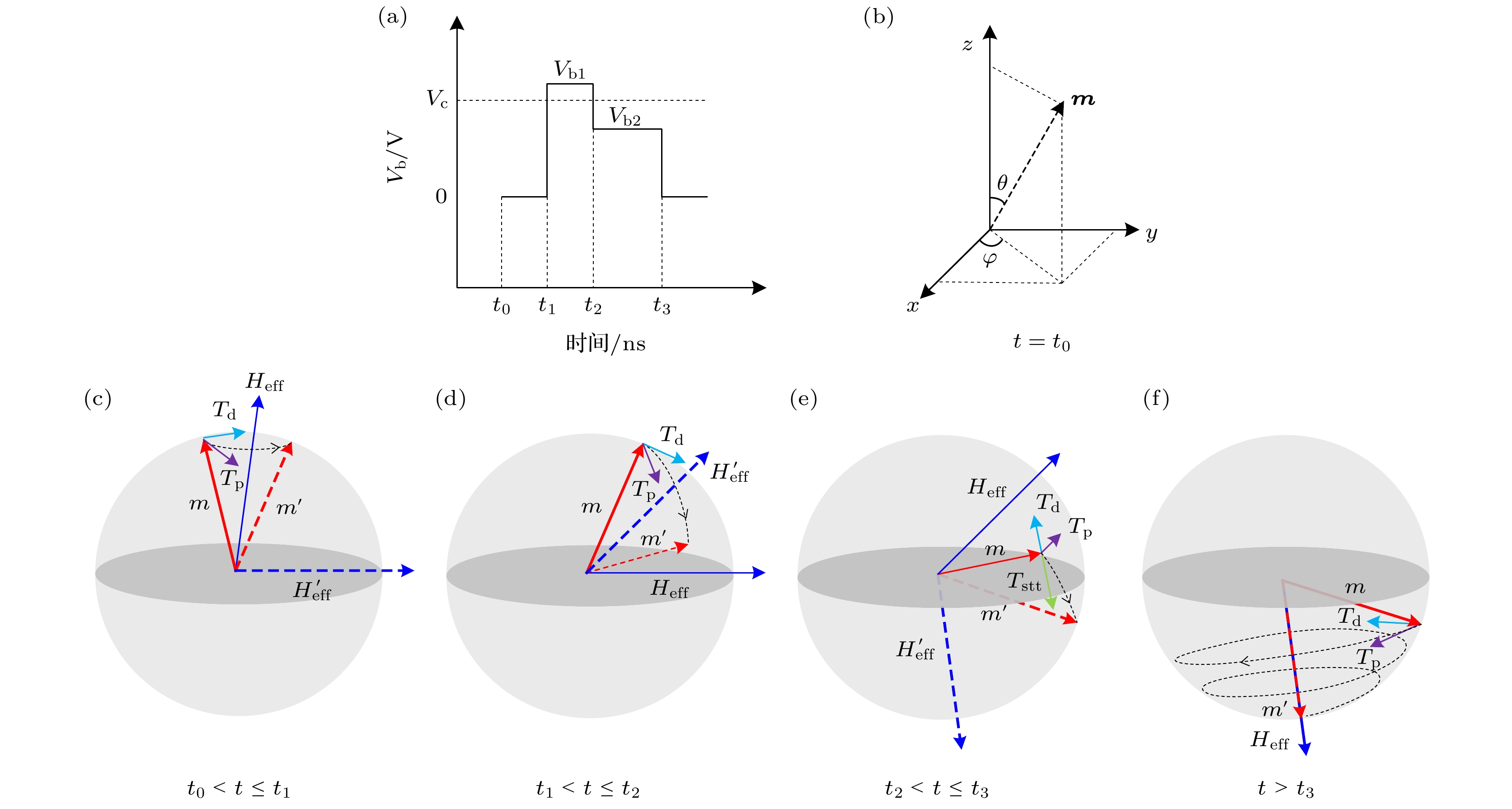
图 3 P态切换到AP态时STT辅助VCMA-MTJ磁化动力学示意图
Fig. 3. Illustration of magnetization dynamics when STT assisted VCMA-MTJ switches from P state to AP state.
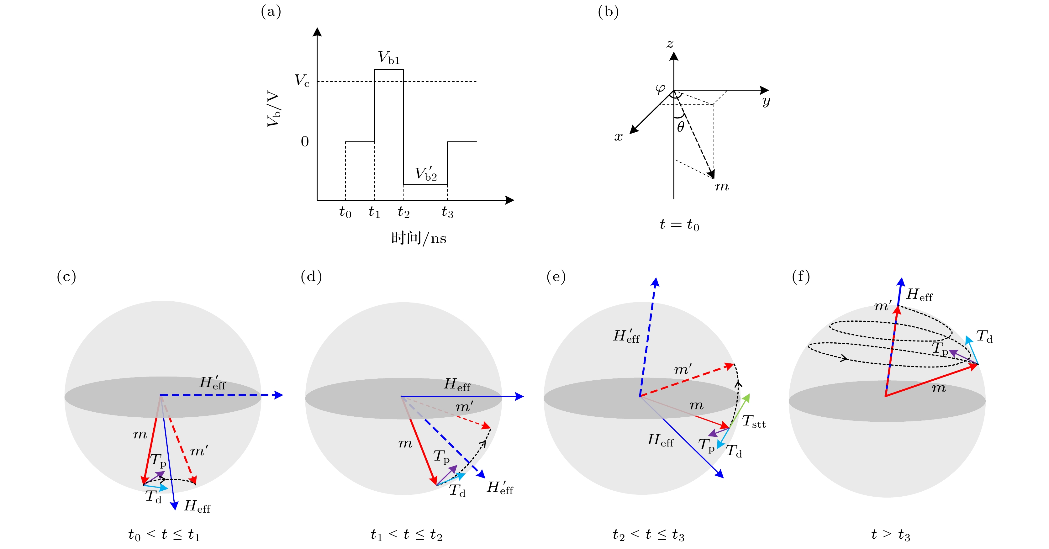
图 4 AP态切换到P态时STT辅助VCMA-MTJ磁化动力学示意图
Fig. 4. Illustration of magnetization dynamics when STT assisted VCMA-MTJ switches from AP state to P state.
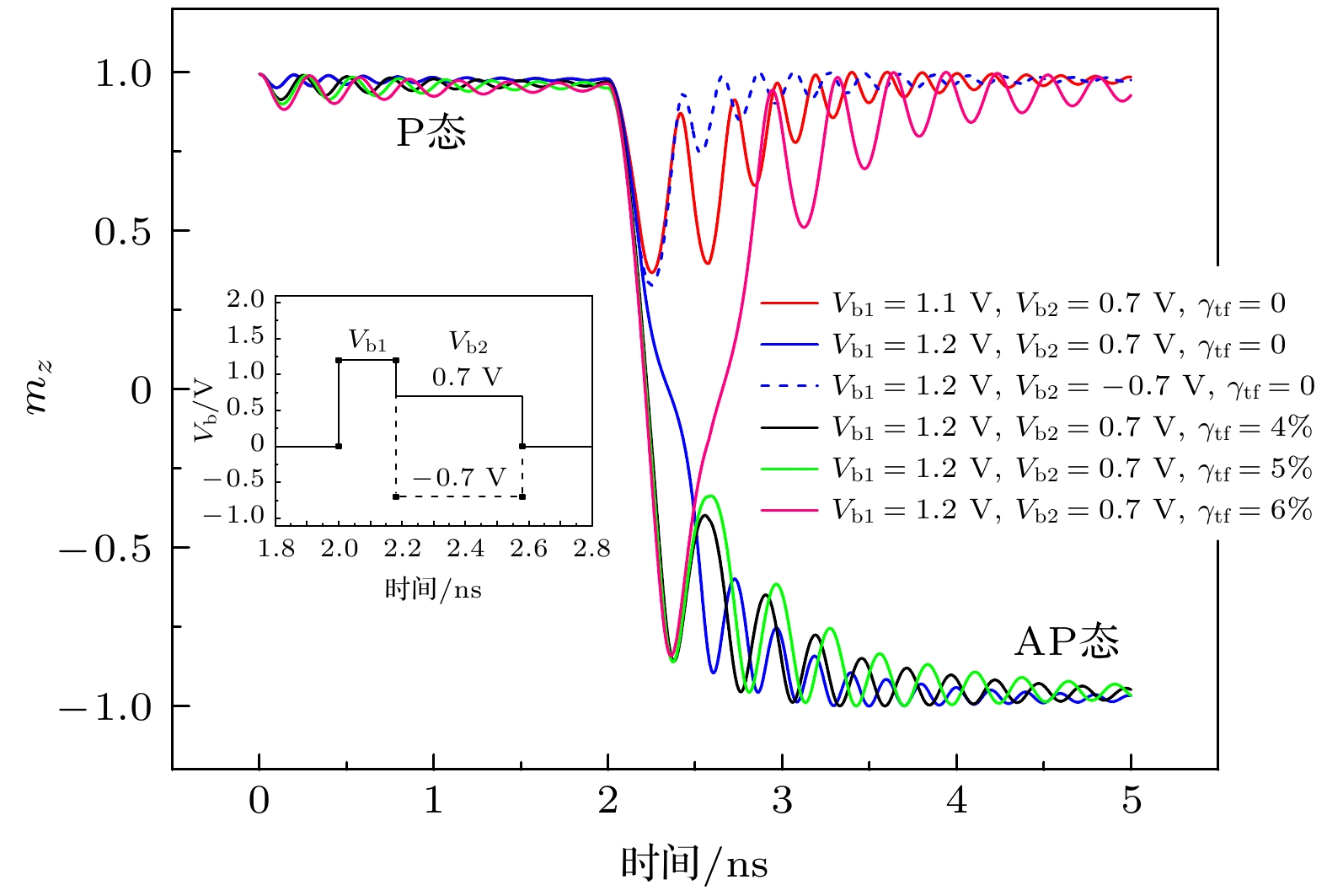
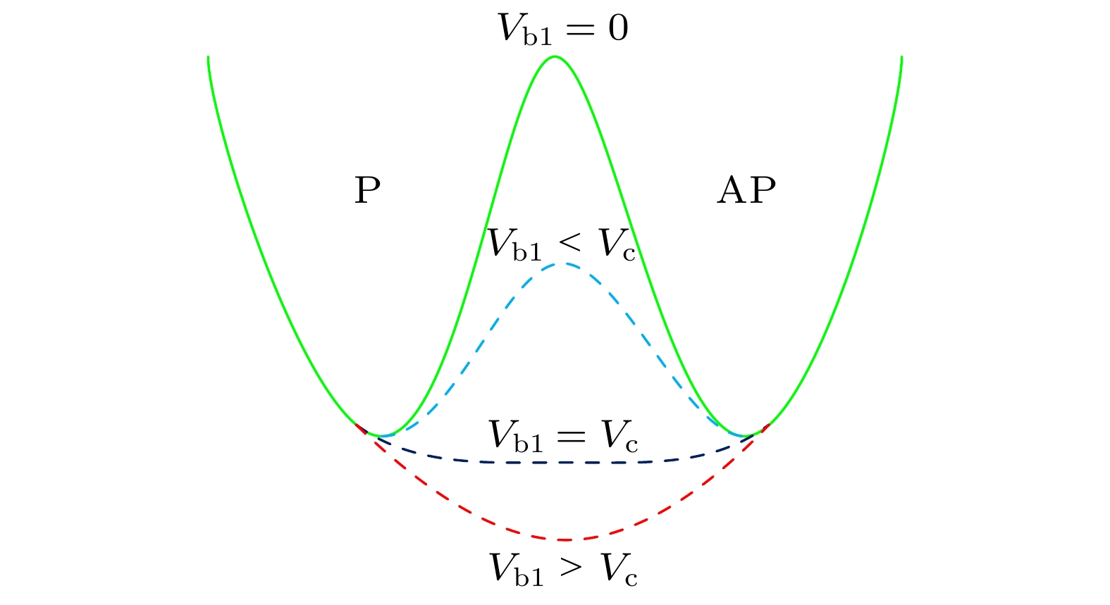
图 5 Vb1, Vb2及γtf对STT辅助VCMA-MTJ状态切换的影响, 其中插图是Vb的设置
Fig. 5. Effects of Vb1, Vb2 and γtf on the state switching of STT assisted VCMA-MTJ, in which the inset represents the setting of Vb.

图 6 γtox对STT辅助VCMA-MTJ状态切换的影响, 其中插图是Vb的设置
Fig. 6. Effect of γtox on the state switching of STT assisted VCMA-MTJ, in which the inset represents the setting of Vb.
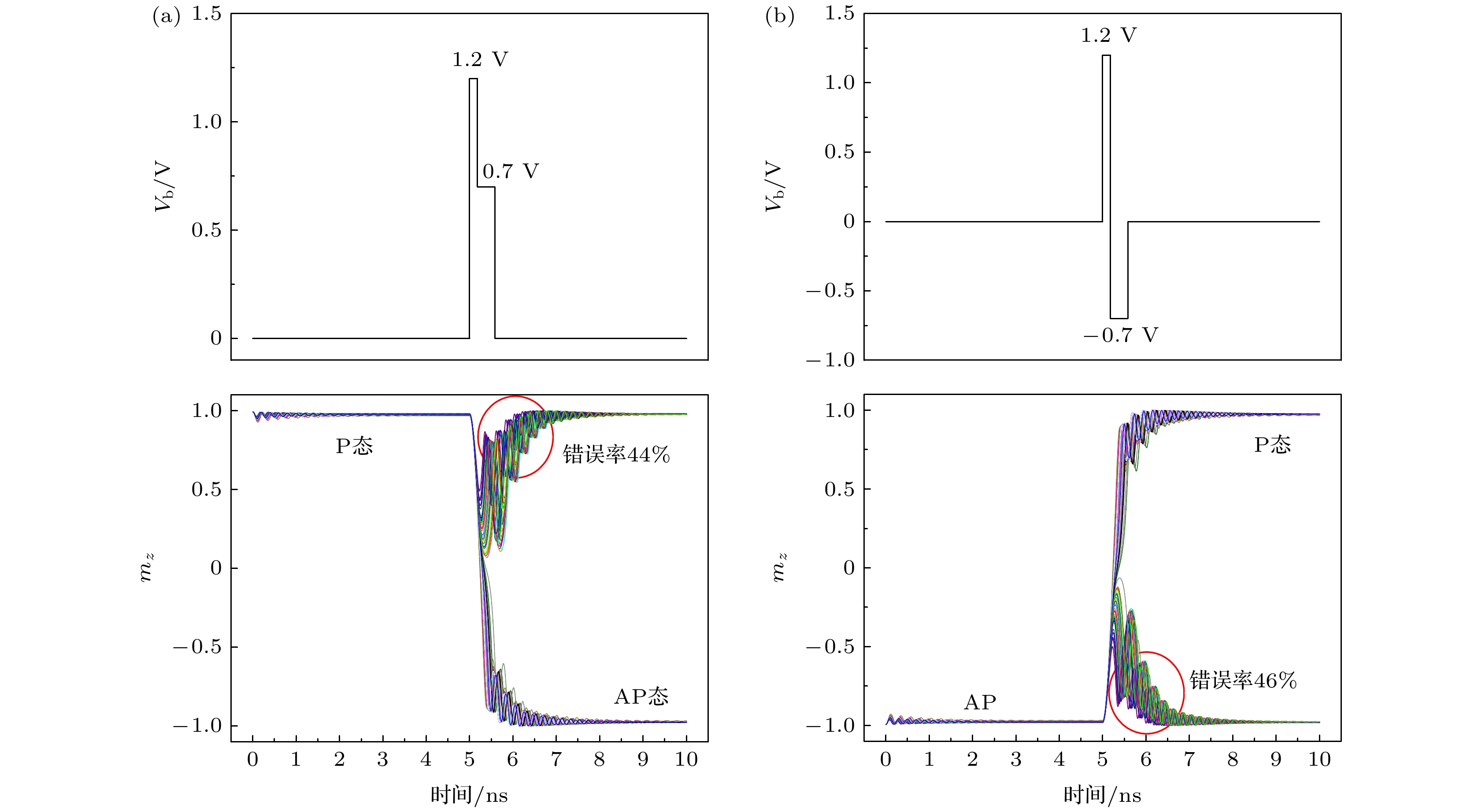
图 11 STT辅助VCMA-MTJ写电路的蒙特卡罗仿真波形 (a)写‘0’; (b)写‘1’
Fig. 11. Monte Carlo simulation waveform of the writing circuit of STT assisted VCMA-MTJ: (a) Writing ‘0’; (b) writing ‘1’.

图 12 写入错误率随Vb1和Vb2的变化 (a)写‘0’的错误率; (b)写‘1’的错误率
Fig. 12. Writing error rate versus Vb1 and Vb2: (a) Writing ‘0’; (b) writing ‘1’.
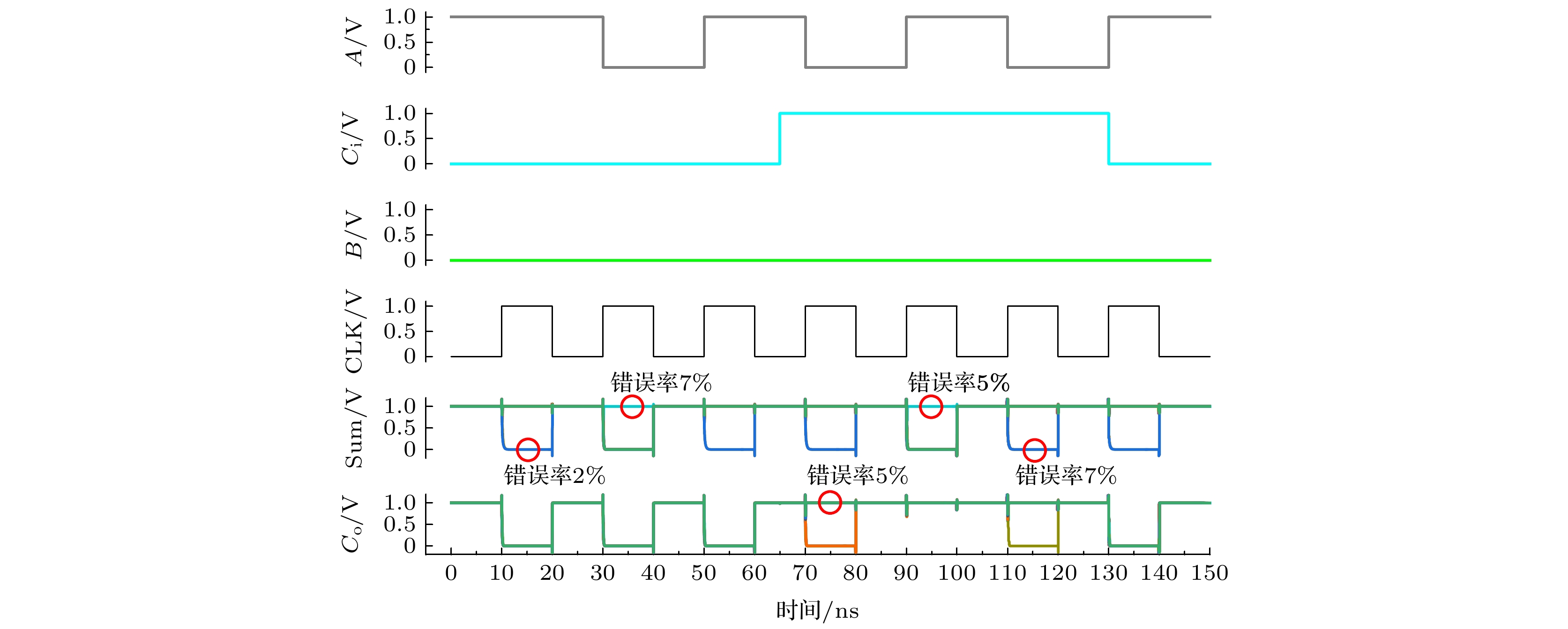
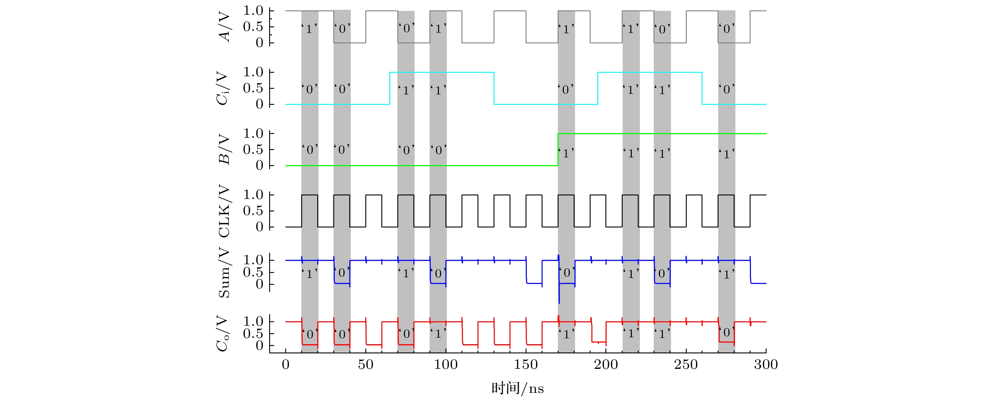
图 13 NV-FA的蒙特卡罗仿真波形, 其中n = 100, 3σ/μ = 0.03, Vdd = 1.0 V
Fig. 13. Monte Carlo simulation waveform of NV-FA with n = 100, 3σ/μ = 0.03, Vdd = 1.0 V.
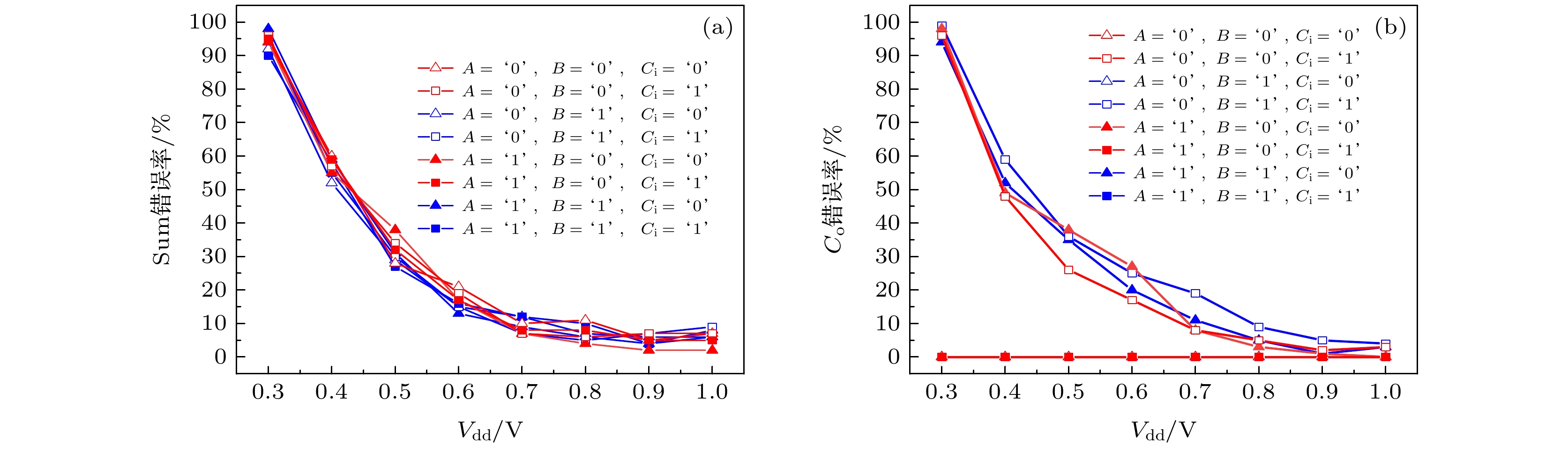
图 14 不同信号下错误率随Vdd的变化 (a) Sum错误率; (b) Co错误率
Fig. 14. Error rate versus Vdd under different signals: (a) Error rate of Sum; (b) error rate of Co.
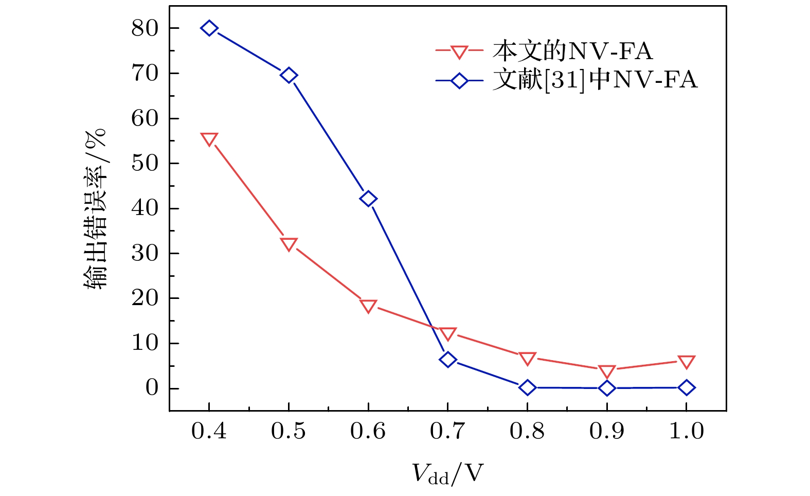
图 15 两款NV-FA输出错误率随Vdd变化情况的比较
Fig. 15. The sensing error rate versus Vdd in two types of NV-FA.
表 1 STT辅助VCMA-MTJ电学模型部分参数列表
Table 1. Partial parameters of the STT assisted VCMA-MTJ model.
参数 符号 值 自由层厚度标准值 tf 1.1 nm 氧化层厚度标准值 tox 1.4 nm MTJ横截面直径 d 50 nm Gilbert阻尼系数 α 0.05 STT极化因子 P 0.58 饱和磁化强度 Ms 0.625 × 10⁶ A/m 垂直磁各向异性系数 Ki 0.32 mJ/m2 VCMA系数 ξ 60 fJ/(V·m) 氧化层势垒高度 $ \bar \varphi $ 0.4 eV 隧穿磁阻率标准值 TMR 100% 外磁场在x轴分量 Hx 31830 A/m x, y轴退磁因子 Nx, y 0.0168 z轴退磁因子 Nz 0.966 旋磁比 γ 2.21 × 10⁵ m/(A·s) 拟合系数 F 11.2727 (m·Ω·eV1/2)–1 拟合因子 Ce 1.025 (m·eV1/2)–1  下载: 导出CSV
-
[1] Verma G 2020 Global Conference on Wireless and Optical Technologies (GCWOT) Malaga, Spain, October 6–8, 2020 p1
[2] Deng E Y, Zhang Y, Klein J O, Ravelsona D, Chappert C, Zhao W S 2013 IEEE Trans. Magn. 49 4982
Google Scholar
[3] Cai H, Jiang H L, Han M L, Wang Z H, Wang Y, Yang J, Han J, Liu L B, Zhao W S 2019 IEEE Computer Society Annual Symposium on VLSI (ISVLSI) Miami, USA, July 1, 2019 p111
[4] Shreya S, Jain A, Kaushik B K 2020 Microelectron. J. 109 104943
Google Scholar
[5] Roohi A, Zand R, Fan D, DeMara R F 2017 IEEE Trans. Comput. AD. D. 36 2134
Google Scholar
[6] Sharmin S, Jaiswal A, Roy K 2016 IEEE Trans. Electron. Devices 63 3493
Google Scholar
[7] Wang Y, Cai H, Naviner L, Zhang Y, Zhao X X, Deng E Y, Klein J O, Zhao W S 2016 IEEE Trans. Electron. Devices 63 1762
Google Scholar
[8] Long M Z, Zeng L, Gao T Q, Zhang D M, Qin X W, Zhang Y G, Zhao W S 2018 IEEE Trans. Nanotechnol. 17 492
Google Scholar
[9] Kanai S, Nakatani Y, Yamanouchi M, Ikeda S, Sato H, Matsukura F, Ohno H 2014 Appl. Phys. Lett. 104 212406
Google Scholar
[10] Zarei A, Safaei F 2018 Microelectron. J. 82 62
Google Scholar
[11] Wang Y, Cai H, Naviner L, Zhao X X, Zhang Y, Slimani M, Klein J O, Zhao W S 2016 Microelectron. Reliab. 64 26
Google Scholar
[12] Meng H, Lum W H, Sbiaa R, Lua S Y H, Tan H K 2011 J. Appl. Phys. 110 033904
Google Scholar
[13] Chun S W, Kim D, Kwon J 2012 J. Appl. Phys. 111 07C722
Google Scholar
[14] Jeong J, Endoh T 2017 Jpn. J. Appl. Phys. 56 04CE09
Google Scholar
[15] Ji M H, Pan L, Hu Y G, Pan M C, Yang L, Peng J P, Qiu W C, Hu J F, Zhang Q, Li P S 2019 AIP Adv. 9 085317
Google Scholar
[16] Amiri P K, Alzate J G, Cai X Q, Ebrahimi F, Hu Q, Wong K, Grezes C, Lee H, Yu G Q, Li X, Akyol M, Shao Q M, Katine J A, Langer J, Ocker B, Wang K L 2015 IEEE Trans. Magn. 51 1
Google Scholar
[17] Liu Y W, Zhang Z Z 2013 Sci. China Phys. Mech. 56 184
Google Scholar
[18] Niranjan M K, Duan C G, Jaswal S S, Tsymbal E V 2010 Appl. Phys. Lett. 96 222504
Google Scholar
[19] Zhao W S, Zhao X X, Zhang B Y, Cao K H, Wang L Z, Kang W, Shi Q, Wang M X, Zhang Y, Wang Y, Peng S Z, Klein J O, Naviner L, Ravelosona D 2016 Materals 9 41
Google Scholar
[20] Kang W, Ran Y, Zhang Y G, Lv W F, Zhao W S 2017 IEEE Trans. Nanotechnol. 16 387
Google Scholar
[21] Brinkman W F, Dynes R C, Rowell J M 1970 J. Appl. Phys. 41 1915
Google Scholar
[22] 金冬月, 陈虎, 王佑, 张万荣, 那伟聪, 郭斌, 吴玲, 杨绍萌, 孙晟 2020 物理学报 69 198502
Google Scholar
Jin D Y, Chen H, Wang Y, Zhang W R, Na W C, Guo B, Wu L, Yang S M, Sun S 2020 Acta Phys. Sin. 69 198502
Google Scholar
[23] Gajek M, Nowak J J, Sun J Z, Trouilloud P L, O’Sullivan E J, Abraham D W, Gaidis M C, Hu G, Brown S, Zhu Y, Robertazzi R P, Gallagher W J 2012 Appl. Phys. Lett. 100 132408
Google Scholar
[24] Chen E, Schwarz B, Choi C J, Kula W, Wolfman J, Ounadjela K, Geha S 2003 J. Appl. Phys. 93 8379
Google Scholar
[25] Wu L Z, Taouil M, Rao S, Marinissen E J, Hamdioui S 2018 IEEE International Test Conference (ITC) Phoenix, USA, October 29–November 1, 2018 p18412682
[26] Sugiura K, Takahashi S, Amano M, Kajiyama T, Iwayama M, Asao Y, Shimomura N, Kishi T, Ikegawa S, Yoda H, Nitayama A 2009 Jpn. J. Appl. Phys. 48 08HD02
Google Scholar
[27] Kinoshita K, Utsumi H, Suemitsu K, Hada H, Sugibayashi T 2010 Jpn. J. Appl. Phys. 49 08JB02
Google Scholar
[28] Kinoshita K, Yamamoto T, Honjo H, Kasai N, Ikeda S, Ohno H 2012 Jpn. J. Appl. Phys. 51 08HA01
Google Scholar
[29] Deng E Y, Wang Y, Wang Z H, Klein J O, Dieny B, Prenat G, Zhao W S 2015 Proceedings of the 2015 IEEE/ACM International Symposium on Nanoscale Architectures Boston, USA, July 8–10, 2015 p27
[30] Li J, Augustine C, Salahuddin S, Roy K 2008 Proceedings of the 45th annual Design Automation Conference New York, USA, June 8–13, 2008 p278
[31] Cai H, Wang Y, Naviner L, Zhao W S 2017 IEEE T. Circuits-I 64 847
Google Scholar

 下载:
下载:


计量
- 文章访问数: 7806
- PDF下载量: 82
- 被引次数: 0
