


-
本文在室温下利用射频磁控溅射技术在(001)蓝宝石衬底上制备了不同厚度的β-Ga2O3薄膜, 随后将其置于氩气气氛中800 ℃退火1 h. 利用XRD, SEM, UV-Vis分光光度计、PL光致发光光谱仪和Keithley 4200-SCS半导体表征系统等考察薄膜厚度对所得氧化镓薄膜相组成、表面形貌、光学性能以及光电探测性能的影响.结果表明, 随着薄膜厚度的增加, 薄膜结晶质量提高, 840 nm薄膜最佳, 1050 nm薄膜结晶质量略有降低. 不同厚度β-Ga2O3薄膜在波长200—300 nm日盲区域内均具有明显的紫外光吸收, 禁带宽度随着薄膜厚度的增加而增加. PL谱中各发光峰峰强随着薄膜厚度的增加而减小, 表明氧空位及其相关缺陷受到抑制. 在β-Ga2O3薄膜基础上制备出日盲紫外光电探测器的探测性能(光暗电流比, 响应度, 探测率, 外量子效率)也随薄膜厚度的增加呈先增后减的趋势. 厚度约为840 nm的β-Ga2O3紫外光电探测器, 在5V偏压下, 表现出极低的暗电流(4.9 × 10⁻¹² A), 以及在波长254 nm (600 μW/cm2) 紫外光照下, 表现出较高的光暗电流比(3.2 × 10⁵), 较短的响应时间0.09/0.80 s (上升时间), 0.06/0.53 s (下降时间), 其响应度、探测率和外量子效率分别为1.19 mA/W, 1.9 × 10¹¹ Jones和0.58%, 且其光电流随光功率密度和偏置电压的增加几乎呈现线性增加, 可以用于制作日盲紫外探测器.In this work, β-Ga2O3 films with different thickness are prepared on (001) sapphire substrates at room temperature by the radio frequency magnetron sputtering technology, then the samples are annealed in an Ar atmosphere at 800 ℃ for 1h. The effects of film thickness on the phase composition, surface morphology, optical property, and photoelectric detection performance are investigated using XRD, SEM, UV-Vis spectrophotometer, PL photoluminescence spectrometer, and Keithley 4200-SCS semiconductor characterization system. The results show that as the film thickness increases, the film crystallinity is improved, films with a thickness of 840 nm exhibit best quality, while those with a thickness of 1050 nm declines a little in quality. The β-Ga2O3 films with different thickness exhibit obvious ultraviolet light absorption in the solar-blind region with wavelengths of 200–300 nm, and the bandgap width increases with the film thickness increasing. All the β-Ga2O3 films show a broad UV-green light emission peaks in a wavelength range of 350–600 nm. As the film thickness increases, the intensities of the emission peaks of ultraviolet, violet, and blue light are greatly reduced, indicating that oxygen vacancy-related defects (VO, VGa–VO) are greatly suppressed with film thickness increasing. Solar-blind ultraviolet photodetector is fabricated based on the β-Ga2O3 film. Its photoelectric detection performances (the photo-to-dark current ratio, responsivity, detectivity, and external quantum efficiency) also increase first and decrease then with the increase of film thickness. The β-Ga2O3 ultraviolet photodetector prepared by a thin film with a thickness of 840 nm exhibits a very low dark current (4.9 × 10⁻¹² A) under a 5 V bias voltage and an ultraviolet light with a wavelength of 254 nm (600 μW/cm2). It exhibits a high photo-to-dark current ratio of 3.2 × 10⁵, and a short response time of 0.09/0.80 s (rising time) and 0.06/0.53 s ratio (falling time). Its responsivity (R), detectivity (D *), and the external quantum efficiency (EQE) are 1.19 mA/W, 1.9 × 10¹¹ Jones, and 0.58%, respectively. The prepared device has quantifiable characteristics, and its photocurrent increases almost linearly with the increase of applied voltage and optical power density, and therefore can work in a linear dynamic region, which indicates that it is very suitable for fabricating the solar-blind ultra-violet detectors.
-
Keywords:
- β-Ga2O3 films /
- solar-blind UV detector /
- film thickness /
- photoelectric detection performance
[1] Chen H Y, Liu K W, Hu L F, Al-Ghamdi A A, Fang X S 2015 Mater. Today 18 493
 Google Scholar
[2] 时浩泽 2018 硕士学位论文 (浙江: 浙江理工大学)
Shi H Z 2018 M. S. Thesis (Zhejiang: Zhejiang Sci-Tech University) (in Chinese)
[3] 郭道友, 李培刚, 陈政委, 吴真平, 唐为华 2019 物理学报 68 078501
Google Scholar
Guo D Y, Li P G, Chen Z W, Wu Z P, Tang W H 2019 Acta Phys. Sin. 68 078501
Google Scholar
[4] 马海林, 苏庆 2014 物理学报 63 116701
Google Scholar
Ma H L, Su Q 2014 Acta Phys. Sin. 63 116701
Google Scholar
[5] 陈彦成 2019 硕士学位论文 (河南: 郑州大学)
Chen Y C 2019 M. S. Thesis (Henan: Zhengzhou University) (in Chinese)
[6] 崔书娟 2018 硕士学位论文 (北京: 中国科学院大学)
Cui S J 2018 M. S. Thesis (Beijing: University of Chinese Academy of Sciences) (in Chinese)
[7] Han S, Huang X L, Fang M Z, Zhao W G, Xu S J, Zhu D L, Xu W Y, Fang M, Liu W J, Cao P J, Lu Y M 2019 J. Mater. Chem. C 7 11834
Google Scholar
[8] Guo D Y, Wu Z P, Li P G, An Y H, Liu H, Guo X C, Yan H, Wang G F, Sun C L, Li L H, Tang W H 2014 Opt. Mater. Express 4 1067
Google Scholar
[9] Shen H, Baskaran K, Yin Y N, Tian K, Duan L B, Zhao X R, Tiwari A 2020 J. Alloys Compd. 822 153419
Google Scholar
[10] Yang H, Liu Y, Luo X G, Li Y, Wu D S, He K Y, Feng Z C 2019 Superlattices Microstruct. 131 21
Google Scholar
[11] Zhang X Y, Wang L, Wang X D, Chen Y, Shao Q Q, Wu G G, Wang X Y, Lin T, Shen H, Wang J L, Meng X J, Chu J H 2020 Opt. Express 28 4169
Google Scholar
[12] An Y H, Zhi Y S, Cui W, Zhao X L, Wu Z P, Guo D Y, Li P G, Tang W H 2017 J. Nanosci. Nanotechnol. 17 9091
Google Scholar
[13] 李世韦 2021 硕士学位论文 (福建: 厦门理工学院)
Li S W 2021 M. S. Thesis (Fujian: Xiamen University of Technology) (in Chinese)
[14] 郑树文, 范广涵, 何苗, 赵灵智 2014 物理学报 63 057102
Google Scholar
Zheng S W, Fan G H, He M, Zhao L Z 2014 Acta Phys. Sin. 63 057102
Google Scholar
[15] Shi Q, Wang Q G, Zhang D, Wang Q L, Li S H, Wang W J, Fan Q L, Zhang J Y 2019 J. Lumin. 206 53
Google Scholar
[16] 周树仁, 张红, 莫慧兰, 刘浩文, 熊元强, 李泓霖, 孔春阳, 叶利娟, 李万俊 2021 物理学报 70 178503
Google Scholar
Zhou S R, Zhang H, Mo H L, Liu H W, Xiong Y Q, Li H L, Kong C Y, Ye L J, Li W J 2021 Acta Phys. Sin. 70 178503
Google Scholar
[17] Mi W, Ma J, Luan C N, Xiao H D 2014 J. Lumin. 146 1
Google Scholar
[18] 马腾宇, 李万俊, 何先旺, 胡慧, 黄利娟, 张红, 熊元强, 李泓霖, 叶利娟, 孔春阳 2020 物理学报 69 108102
Google Scholar
Ma T Y, Li W J, He X W, Hu H, Huang L Y, Zhang H, Xiong Y Q, Li H L, Ye L J, Kong C Y 2020 Acta Phys. Sin. 69 108102
Google Scholar
[19] Yang Y, Zhang P 2010 Phys. Lett. A 374 4169
Google Scholar
[20] Wei J Y, Shi F 2016 J. Mater. Sci. Mater. Electron. 27 942
Google Scholar
[21] Vanithakumari S C, Nanda K K 2009 Phosphors. Adv. Mater. 21 3581
Google Scholar
[22] 祁祺, 陈海峰, 洪梓凡, 刘英英, 过立新, 李立珺, 陆芹, 贾一凡 2020 物理学报 69 168101
Google Scholar
Qi Q, Chen H F, Hong Z F, Liu Y Y, Guo L X, Li L J, Lu Q, Jia Y F 2020 Acta Phys. Sin. 69 168101
Google Scholar
[23] Liu L L, Li M K, Yu D Q, Zhang J, Zhang H, Qian C, Yang Z 2010 Appl. Phys. A 9 831
[24] Huan Y W, Sun S M, Gu C J, Ding S J, Yu S Y, Liu W J, Ding S J, Yu H Y, Xia C T, Zhang D W 2018 Nanoscale Res. Lett. 13 246
Google Scholar
[25] 雷挺, 吕伟明, 吕文星, 崔博垚, 胡瑞, 时文华, 曾中明 2021 物理学报 70 027801
Google Scholar
Lei T, Lü W M, Lü W X, Cui B Y, Hu R, Shi W H, Zeng Z M 2021 Acta Phys. Sin. 70 027801
Google Scholar
[26] Tak B R, Garg M, Kumar A, Gupta V, Singh R 2019 ECS J. Solid State Sci. Technol. 8 Q3149
Google Scholar
[27] Razeghi M, Rogalski A 1996 J. Appl. Phys. 79 7433
Google Scholar
[28] Fang Y, Armin A, Meredith P, Huang J S 2019 Nat. Photonics 13 1
Google Scholar
[29] Kaur D, Kumar M 2021 Adv. Opti. Mater. 9 2002160
Google Scholar
[30] Liu Z, Zhi Y, Li S, Liu Y, Tang X, Yan Z, Li P, Li X, Guo D, Wu Z, Tang W 2020 J. Phys. D:Appl. Phys. 53 085105
Google Scholar
[31] Liu Z, Li S, Yan Z, Liu Y, Zhi Y, Wang X, Wu Z, Li P, Tang W 2020 J. Mater. Chem. C 8 5071
Google Scholar
[32] Zhi Y S, Jiang W Y, Liu Z, Liu Y Y, Chu X L, Liu J H, Li S, Yan Z Y, Wang Y H, Li P G, Wu Z P, Tang W H 2021 Chin. Phys. B 30 057301
Google Scholar
[33] Wang J, Ye L J, Wang X, Zhang H, Li L, Kong C, Li W J 2019 J. Alloys Compd. 803 9
Google Scholar
[34] Zhang D, Zheng W, Lin R C, Li T T, Zhang Z J, Huang F 2018 J. Alloys Compd. 735 150
Google Scholar
[35] Tak B R, Garg M, Dewan S, Torres-Castanedo C G, Li K H, Gupta V, Li X H, Singh R 2019 J. Appl. Phys. 125 144501
Google Scholar
[36] Qian L X, Wu Z H, Zhang Y Y, Lai P T, Liu X Z, Li Y R 2017 ACS Photonics 4 2203
Google Scholar
[37] Yu M, Lv C D, Yu J G, Shen Y M, Yuan L, Hu J C, Zhang S G, Cheng H J, Zhang Y M, Jia R X 2020 Mater. Today Commun. 25 101532
Google Scholar
-

图 1 β-Ga2O3薄膜的SEM图像 (a)断面; (b)—(d)表面形貌
Fig. 1. SEM images of the β-Ga2O3 films: (a) Cross-section; (b)–(d) morphology and surface morphology.
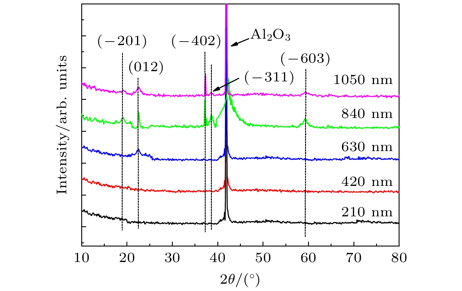
图 2 不同厚度β-Ga2O3薄膜的XRD图谱
Fig. 2. XRD patterns of β-Ga2O3 films with different thicknesses.

图 3 (a)不同厚度β-Ga2O3薄膜的UV-Vis吸收光谱; (b)β-Ga2O3薄膜α2随hν的变化曲线; (c)不同厚度β-Ga2O3薄膜的光学带隙(Eg)图
Fig. 3. (a) UV-Vis absorption spectra of β-Ga2O3 thin films with different thicknesses; (b) plot of absorption coefficient vs. photon energy of the β-Ga2O3 films; (c) dependence of optical band gap (Eg) on thickness of the β-Ga2O3 films.
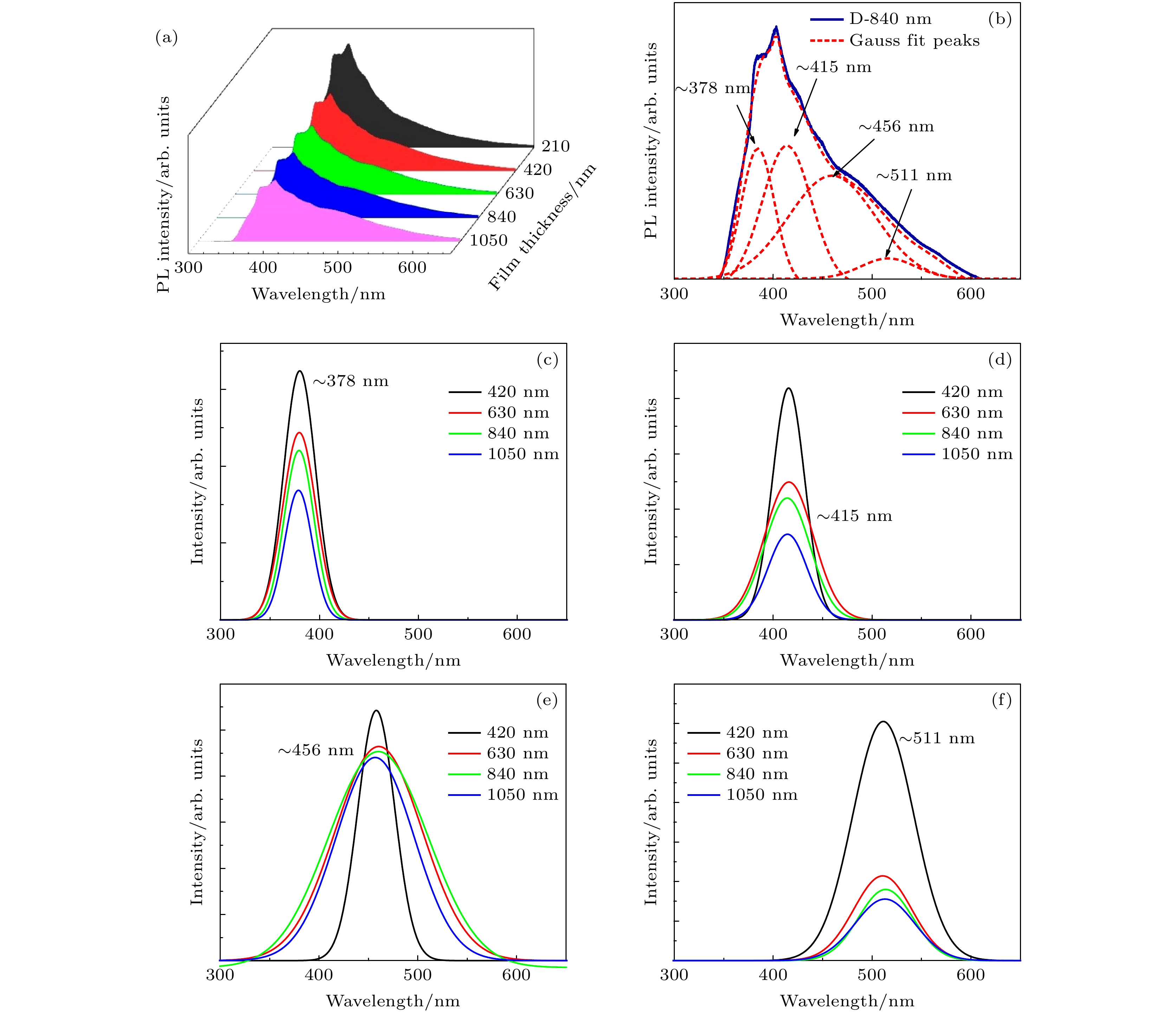
图 4 (a)不同薄膜厚度的β-Ga2O3薄膜的PL光谱; (b)薄膜厚度约为840 nm的Ga2O3薄膜的PL高斯拟合峰; (c)—(f)分别显示了不同厚度Ga2O3薄膜在波长约为378, 415, 456和511 nm处的PL拟合峰
Fig. 4. (a) PL spectrum of the β-Ga2O3 films with different thicknesses; (b) PL Gaussian fitting peak of the β-Ga2O3 film with a thickness of ~840 nm; (c)–(f) respectively shows the PL fitting peaks at ~378, ~415, ~456 and ~511 nm of the β-Ga2O3 films.

图 5 (a) β-Ga2O3紫外光电探测器层结构示意图; (b)不同薄膜厚度β-Ga2O3 器件的I-t图; (c), (d) A和D器件瞬态响应曲线的局部放大图
Fig. 5. (a) Schematic diagram of the β-Ga2O3 ultraviolet photodetector layer structure; (b) I-t curves of the devices based on β-Ga2O3 films with different thicknesses; (c), (d) magnification diagrams of the transient response curves of the device A and D.
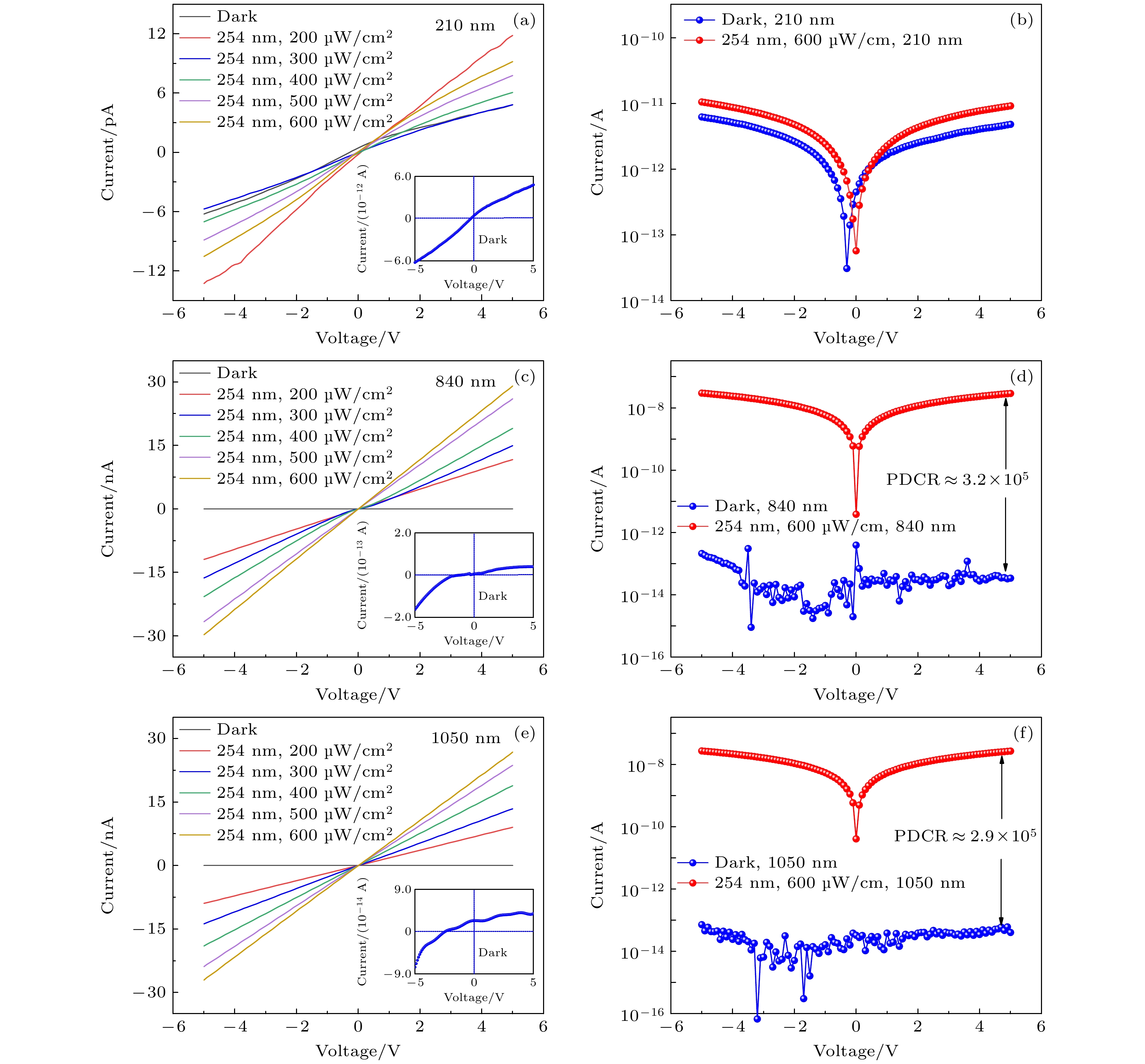
图 6 (a), (c), (e)为不同器件的I-V曲线, 其中插图为暗电流与电压关系的放大图; (b), (d), (f)为不同器件的光暗电流对数坐标图
Fig. 6. (a), (c), (e) I-V curves of device A, D and E, respectively. The insets are the enlarged view of the relationship between dark current and voltage. (b), (d), (f) Logarithmic graphs of photo and dark current of device A, D and E, respectively.
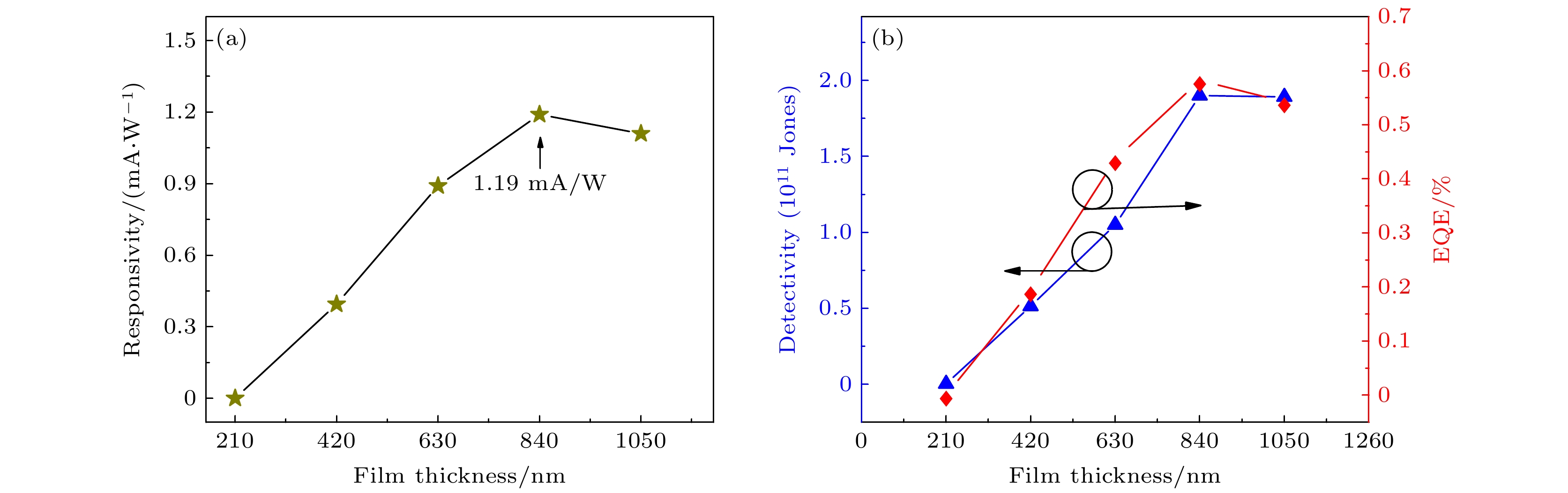
图 7 器件的薄膜厚度与(a)响应度R的关系曲线以及(b)与探测率D*, EQE的关系曲线
Fig. 7. (a) Relationship curve between the responsivity (R) and film thickness; (b) relationship curve between the D* & EQE and film thickness.
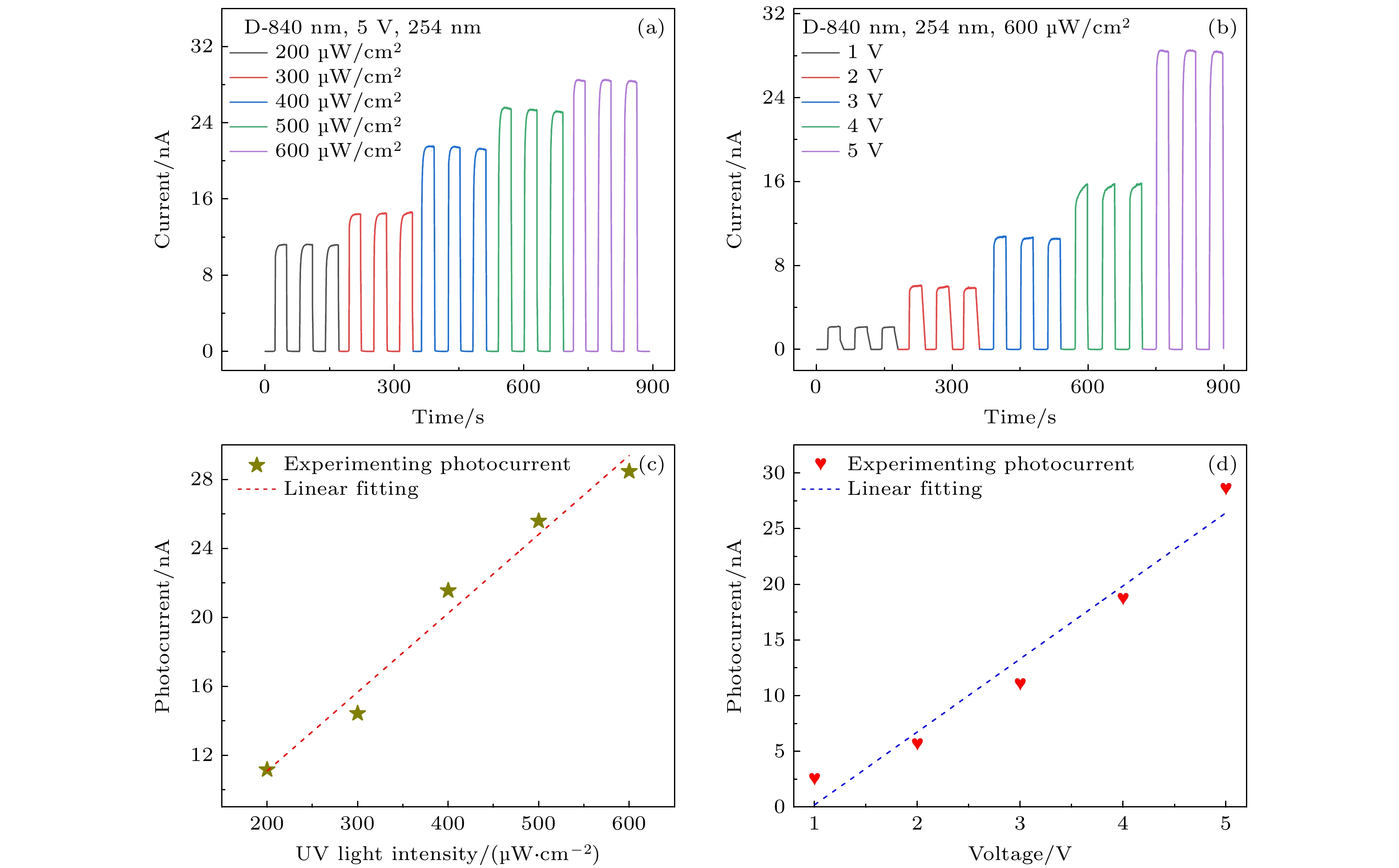
图 8 (a) D器件在不同光功率密度光照下I-t图; (b) D器件在不同偏压下的I-t图; (c)光电流与光功率密度的关系; (d)光电流与外加偏压的关系
Fig. 8. (a) I-t graph of D device under the illumination with different power densities; (b) I-t graph of D device under different bias voltages; (c) relationship between photocurrent and optical power density; (d) relationship between photocurrent and applied bias voltage.
表 1 β-Ga2O3薄膜的厚度
Table 1. Thickness of β-Ga2O3 film.
沉积时间/min 10 20 30 40 50 薄膜厚度/nm ~210 ~420 ~630 ~840 ~1050  下载: 导出CSV
表 2 不同器件的光响应时间汇总表
Table 2. Summary table of photo-response time of the device A to E.
器件名 A B C D E 上升时间 τr1/τr2 /s 0.35/3.14 0.21/2.57 0.15/1.69 0.09/0.80 0.07/0.69 下降时间 τd1/τd2 /s 0.16/0.68 0.13/0.61 0.09/0.58 0.06/0.53 0.05/0.48
下载: 导出CSV
表 3 国内外Ga2O3薄膜基光电探测器的主要性能指标对比
Table 3. Comparison of the representative photoresponse metrics of the photodetectors based on Ga2O3 films.
Samples Growth Bias /V Idark /nA τr /s τd/s PDCR R/ (A·W–1) Ref. β-Ga2O3 Sputtering 10 0.11 0.31/1.52 0.05/0.91 >103 — [33] β-Ga2O3 MOCVD 10 34 0.48 0.18 ~104 26.1 [34] β-Ga2O3 Sputtering 5 0.1 1.0/1.4 1.2/1.3 — — [12] Ga2O3 PLD 20 ~0.0001 0.004 0.104 ~108 0.0003 [11] β-Ga2O3 PLD 10 ~1.2 0.59/2.4 0.15/1.6 ~103 0.74 [35] α-Ga2O3 Sputtering 10 0.3386 0.41/2.04 0.02/0.35 — 70.26 [36] α/β-Ga2O3 Sol-gel 15 0.125 0.04/0.87 0.02/1.00 ~1.7×10 0.0177 [37] β-Ga2O3 Sputtering 10 0.56 0.51/3.04 0.07/0.08 — 0.028 [16] β-Ga2O3 Sputtering 5 ~0.0049 0.09/0.80 0.06/0.53 ~3.2×10⁵ 0.00119 This work
下载: 导出CSV
-
[1] Chen H Y, Liu K W, Hu L F, Al-Ghamdi A A, Fang X S 2015 Mater. Today 18 493
Google Scholar
[2] 时浩泽 2018 硕士学位论文 (浙江: 浙江理工大学)
Shi H Z 2018 M. S. Thesis (Zhejiang: Zhejiang Sci-Tech University) (in Chinese)
[3] 郭道友, 李培刚, 陈政委, 吴真平, 唐为华 2019 物理学报 68 078501
Google Scholar
Guo D Y, Li P G, Chen Z W, Wu Z P, Tang W H 2019 Acta Phys. Sin. 68 078501
Google Scholar
[4] 马海林, 苏庆 2014 物理学报 63 116701
Google Scholar
Ma H L, Su Q 2014 Acta Phys. Sin. 63 116701
Google Scholar
[5] 陈彦成 2019 硕士学位论文 (河南: 郑州大学)
Chen Y C 2019 M. S. Thesis (Henan: Zhengzhou University) (in Chinese)
[6] 崔书娟 2018 硕士学位论文 (北京: 中国科学院大学)
Cui S J 2018 M. S. Thesis (Beijing: University of Chinese Academy of Sciences) (in Chinese)
[7] Han S, Huang X L, Fang M Z, Zhao W G, Xu S J, Zhu D L, Xu W Y, Fang M, Liu W J, Cao P J, Lu Y M 2019 J. Mater. Chem. C 7 11834
Google Scholar
[8] Guo D Y, Wu Z P, Li P G, An Y H, Liu H, Guo X C, Yan H, Wang G F, Sun C L, Li L H, Tang W H 2014 Opt. Mater. Express 4 1067
Google Scholar
[9] Shen H, Baskaran K, Yin Y N, Tian K, Duan L B, Zhao X R, Tiwari A 2020 J. Alloys Compd. 822 153419
Google Scholar
[10] Yang H, Liu Y, Luo X G, Li Y, Wu D S, He K Y, Feng Z C 2019 Superlattices Microstruct. 131 21
Google Scholar
[11] Zhang X Y, Wang L, Wang X D, Chen Y, Shao Q Q, Wu G G, Wang X Y, Lin T, Shen H, Wang J L, Meng X J, Chu J H 2020 Opt. Express 28 4169
Google Scholar
[12] An Y H, Zhi Y S, Cui W, Zhao X L, Wu Z P, Guo D Y, Li P G, Tang W H 2017 J. Nanosci. Nanotechnol. 17 9091
Google Scholar
[13] 李世韦 2021 硕士学位论文 (福建: 厦门理工学院)
Li S W 2021 M. S. Thesis (Fujian: Xiamen University of Technology) (in Chinese)
[14] 郑树文, 范广涵, 何苗, 赵灵智 2014 物理学报 63 057102
Google Scholar
Zheng S W, Fan G H, He M, Zhao L Z 2014 Acta Phys. Sin. 63 057102
Google Scholar
[15] Shi Q, Wang Q G, Zhang D, Wang Q L, Li S H, Wang W J, Fan Q L, Zhang J Y 2019 J. Lumin. 206 53
Google Scholar
[16] 周树仁, 张红, 莫慧兰, 刘浩文, 熊元强, 李泓霖, 孔春阳, 叶利娟, 李万俊 2021 物理学报 70 178503
Google Scholar
Zhou S R, Zhang H, Mo H L, Liu H W, Xiong Y Q, Li H L, Kong C Y, Ye L J, Li W J 2021 Acta Phys. Sin. 70 178503
Google Scholar
[17] Mi W, Ma J, Luan C N, Xiao H D 2014 J. Lumin. 146 1
Google Scholar
[18] 马腾宇, 李万俊, 何先旺, 胡慧, 黄利娟, 张红, 熊元强, 李泓霖, 叶利娟, 孔春阳 2020 物理学报 69 108102
Google Scholar
Ma T Y, Li W J, He X W, Hu H, Huang L Y, Zhang H, Xiong Y Q, Li H L, Ye L J, Kong C Y 2020 Acta Phys. Sin. 69 108102
Google Scholar
[19] Yang Y, Zhang P 2010 Phys. Lett. A 374 4169
Google Scholar
[20] Wei J Y, Shi F 2016 J. Mater. Sci. Mater. Electron. 27 942
Google Scholar
[21] Vanithakumari S C, Nanda K K 2009 Phosphors. Adv. Mater. 21 3581
Google Scholar
[22] 祁祺, 陈海峰, 洪梓凡, 刘英英, 过立新, 李立珺, 陆芹, 贾一凡 2020 物理学报 69 168101
Google Scholar
Qi Q, Chen H F, Hong Z F, Liu Y Y, Guo L X, Li L J, Lu Q, Jia Y F 2020 Acta Phys. Sin. 69 168101
Google Scholar
[23] Liu L L, Li M K, Yu D Q, Zhang J, Zhang H, Qian C, Yang Z 2010 Appl. Phys. A 9 831
[24] Huan Y W, Sun S M, Gu C J, Ding S J, Yu S Y, Liu W J, Ding S J, Yu H Y, Xia C T, Zhang D W 2018 Nanoscale Res. Lett. 13 246
Google Scholar
[25] 雷挺, 吕伟明, 吕文星, 崔博垚, 胡瑞, 时文华, 曾中明 2021 物理学报 70 027801
Google Scholar
Lei T, Lü W M, Lü W X, Cui B Y, Hu R, Shi W H, Zeng Z M 2021 Acta Phys. Sin. 70 027801
Google Scholar
[26] Tak B R, Garg M, Kumar A, Gupta V, Singh R 2019 ECS J. Solid State Sci. Technol. 8 Q3149
Google Scholar
[27] Razeghi M, Rogalski A 1996 J. Appl. Phys. 79 7433
Google Scholar
[28] Fang Y, Armin A, Meredith P, Huang J S 2019 Nat. Photonics 13 1
Google Scholar
[29] Kaur D, Kumar M 2021 Adv. Opti. Mater. 9 2002160
Google Scholar
[30] Liu Z, Zhi Y, Li S, Liu Y, Tang X, Yan Z, Li P, Li X, Guo D, Wu Z, Tang W 2020 J. Phys. D:Appl. Phys. 53 085105
Google Scholar
[31] Liu Z, Li S, Yan Z, Liu Y, Zhi Y, Wang X, Wu Z, Li P, Tang W 2020 J. Mater. Chem. C 8 5071
Google Scholar
[32] Zhi Y S, Jiang W Y, Liu Z, Liu Y Y, Chu X L, Liu J H, Li S, Yan Z Y, Wang Y H, Li P G, Wu Z P, Tang W H 2021 Chin. Phys. B 30 057301
Google Scholar
[33] Wang J, Ye L J, Wang X, Zhang H, Li L, Kong C, Li W J 2019 J. Alloys Compd. 803 9
Google Scholar
[34] Zhang D, Zheng W, Lin R C, Li T T, Zhang Z J, Huang F 2018 J. Alloys Compd. 735 150
Google Scholar
[35] Tak B R, Garg M, Dewan S, Torres-Castanedo C G, Li K H, Gupta V, Li X H, Singh R 2019 J. Appl. Phys. 125 144501
Google Scholar
[36] Qian L X, Wu Z H, Zhang Y Y, Lai P T, Liu X Z, Li Y R 2017 ACS Photonics 4 2203
Google Scholar
[37] Yu M, Lv C D, Yu J G, Shen Y M, Yuan L, Hu J C, Zhang S G, Cheng H J, Zhang Y M, Jia R X 2020 Mater. Today Commun. 25 101532
Google Scholar
-
[1] 董典萌, 王景晨, 徐笑云, 彭敏, 王泽川, 汪成, 吴真平. 基于背入射技术的全透明β-Ga2O3多模式日盲探测实验系统构建. 物理学报, 2025, 74(22): 225203. doi: 10.7498/aps.74.20251009 [2] 许怡红, 范伟航, 王尘. 退火温度对磁控溅射掺锡氧化镓薄膜特性及其日盲光电探测器性能的影响. 物理学报, 2025, 74(2): 028104. doi: 10.7498/aps.74.20240972 [3] 宜子琪, 王彦明, 王硕, 隋雪, 石佳辉, 杨壹涵, 王德煜, 冯秋菊, 孙景昌, 梁红伟. 基于机械剥离制备的PEDOT:PSS/β-Ga2O3微米片异质结紫外光电探测器研究. 物理学报, 2024, 73(15): 157102. doi: 10.7498/aps.73.20240630 [4] 张裕, 刘瑞文, 张京阳, 焦斌斌, 王如志. 氧化镓悬臂式薄膜日盲探测器及其电弧检测应用. 物理学报, 2024, 73(9): 098501. doi: 10.7498/aps.73.20240186 [5] 宿冉, 奚昭颖, 李山, 张嘉汉, 姜明明, 刘增, 唐为华. 基于GaSe/Ga2O3异质结的自供电日盲紫外光电探测器. 物理学报, 2024, 73(11): 118502. doi: 10.7498/aps.73.20240267 [6] 张茂林, 马万煜, 王磊, 刘增, 杨莉莉, 李山, 唐为华, 郭宇锋. WO3/β-Ga2O3异质结深紫外光电探测器的高温性能. 物理学报, 2023, 72(16): 160201. doi: 10.7498/aps.72.20230638 [7] 刘玮, 冯秋菊, 宜子琪, 俞琛, 王硕, 王彦明, 隋雪, 梁红伟. Cu掺杂β-Ga2O3薄膜的制备及紫外探测性能. 物理学报, 2023, 72(19): 198503. doi: 10.7498/aps.72.20230971 [8] 董典萌, 汪成, 张清怡, 张涛, 杨永涛, 夏翰驰, 王月晖, 吴真平. 基于HfO2插层的Ga2O3基金属-绝缘体-半导体结构日盲紫外光电探测器. 物理学报, 2023, 72(9): 097302. doi: 10.7498/aps.72.20222222 [9] 况丹, 徐爽, 史大为, 郭建, 喻志农. 基于铝纳米颗粒修饰的非晶氧化镓薄膜日盲紫外探测器. 物理学报, 2023, 72(3): 038501. doi: 10.7498/aps.72.20221476 [10] 刘增, 李磊, 支钰崧, 都灵, 方君鹏, 李山, 余建刚, 张茂林, 杨莉莉, 张少辉, 郭宇锋, 唐为华. 具有大光电导增益的氧化镓薄膜基深紫外探测器阵列. 物理学报, 2022, 71(20): 208501. doi: 10.7498/aps.71.20220859 [11] 王波, 张纪红, 李聪颖. 石墨烯增强半导体态二氧化钒近场热辐射. 物理学报, 2021, 70(5): 054207. doi: 10.7498/aps.70.20201360 [12] 玄鑫淼, 王加恒, 毛彦琦, 叶利娟, 张红, 李泓霖, 熊元强, 范嗣强, 孔春阳, 李万俊. 基于云母衬底生长的非晶Ga2O3柔性透明日盲紫外光探测器研究. 物理学报, 2021, 70(23): 238502. doi: 10.7498/aps.70.20211039 [13] 周树仁, 张红, 莫慧兰, 刘浩文, 熊元强, 李泓霖, 孔春阳, 叶利娟, 李万俊. N掺杂对 ${\boldsymbol\beta} $ -Ga2O3薄膜日盲紫外探测器性能的影响. 物理学报, 2021, 70(17): 178503. doi: 10.7498/aps.70.20210434[14] 李秀华, 张敏. 薄膜厚度对射频磁控溅射β-Ga2O3薄膜光电性能的影响*. 物理学报, 2021, (): . doi: 10.7498/aps.70.20211744 [15] 郭道友, 李培刚, 陈政委, 吴真平, 唐为华. 超宽禁带半导体β-Ga2O3及深紫外透明电极、日盲探测器的研究进展. 物理学报, 2019, 68(7): 078501. doi: 10.7498/aps.68.20181845 [16] 祁晓萌, 彭文博, 赵小龙, 贺永宁. 基于高阻ZnO薄膜的光电导型紫外探测器. 物理学报, 2015, 64(19): 198501. doi: 10.7498/aps.64.198501 [17] 王英龙, 张鹏程, 刘虹让, 刘保亭, 傅广生. 晶粒尺寸及衬底应力对铁电薄膜特性的影响. 物理学报, 2011, 60(7): 077702. doi: 10.7498/aps.60.077702 [18] 岂云开, 顾建军, 刘力虎, 张海峰, 徐芹, 孙会元. Al掺杂ZnO薄膜的厚度对其结构及磁学性能的影响. 物理学报, 2011, 60(6): 067502. doi: 10.7498/aps.60.067502 [19] 马丙现, 姚 宁, 贾 瑜, 杨仕娥, 鲁占灵, 樊志琴, 张兵临. 金刚石薄膜的结构特征对薄膜附着性能的影响. 物理学报, 2005, 54(6): 2853-2858. doi: 10.7498/aps.54.2853 [20] 张国勇, 张鹏翔. 测量高温超导YBCO薄膜厚度的一种新方法. 物理学报, 2001, 50(8): 1451-1455. doi: 10.7498/aps.50.1451

 下载:
下载:

计量
- 文章访问数: 10763
- PDF下载量: 185
- 被引次数: 0
