


-
抗辐射嵌入式闪存工艺在航空航天领域应用广泛, 其中高压NMOS器件对总剂量辐射效应最敏感, 对该器件进行加固是提高芯片抗辐射能力的关键之一. 本文采用浅槽隔离(STI)场区离子注入工艺对180 nm嵌入式闪存工艺中的高压NMOS器件进行加固, 实验结果表明该加固器件存在两个主要问题: 1)浅槽刻蚀后进行离子注入, 后续热工艺较多, 存在显著的杂质再分布效应, 导致STI侧壁离子浓度降低, 经过1×10⁵ rad (1 rad = 10–2 Gy)(Si)辐照后, 器件因漏电流增大而无法关断; 2)加固离子注入降低了漏区PN结击穿电压, 不能满足实际应用需求. 为解决上述问题, 本文提出了一种新型部分沟道离子注入加固方案. 该方案调整加固离子注入工艺至热预算较多的栅氧工艺之后, 减弱了离子再分布效应. 另外, 仅在STI边缘的沟道中部进行离子注入, 不影响漏击穿电压. 采用本方案对高压NMOS器件进行总剂量工艺加固, 不改变器件的条形栅设计, 对器件电学参数影响较小, 与通用工艺兼容性好. 测试结果表明, 器件经过1.5×10⁵ rad (Si)总剂量辐照后, 关态漏电流保持在10–12 A左右, 这比传统的STI场区离子注入加固方案降低了5个数量级.Radiation-hardened embedded flash technology is widely used in aerospace field. The high voltage nMOSFET is the key device to be hardened as it is the most sensitive device to total ionizing dose (TID) effect. In this study, the shallow tench isolation (STI) sidewall implantation method is used to harden 5 V nMOSFET for 180 nm eFlash process. Through the study of the TID response of the device, two problems emerge in this hardening technology. Firstly, the hardening ions are implanted after STI trench etching, the doping profile is influenced by the following thermal process, resulting in lower doping concentration at STI edge. The device fails to work due to high leakage current after 1×10⁵ rad (1 rad = 10–2 Gy) (Si) radiation. Secondly, the hardening ions that are implanted in drain region reduce the breakdown voltage of PN junction on the drain side. Device cannot satisfy the actual requirement in the circuit. To solve these problems, we propose a new device hardening method called partial channel ion implantation. Comparing with previous method, in order to reduce the doping redistribution effect, we adjust the hardening ion implantation to an extent after the oxidation of gate oxide. Moreover, an extra mask is introduced to determine the hardening implantation region to avoid ion implantation on the drain side of the device. Therefore, the drain breakdown voltage will not be influenced by hardening implantation. By using this new hardening technology for high voltage NMOS, the device can maintain the typical design of strip-type gate. The hardening method is compatible with general process technology and does not influence the electrical parameters of the device obviously. The results show that with the partial channel ion implantation method, the drain leakage of the device is kept at a pico-ampere level after 1.5×10⁵ rad (Si) radiation. That is five orders of magnitude lower than that obtained by using previous STI implantation hardening technology.
-
Keywords:
- total ionizing dose effect /
- radiation hardening by process /
- high voltage MOSFET /
- embedded flash
[1] Barnaby H J, McLain M L, Sanchez Esqueda I, Chen X J 2009 IEEE Trans. Circuits Syst. Ⅰ 56 1870
 Google Scholar
[2] 卓青青, 刘红侠, 杨兆年, 蔡慧民, 郝跃 2012 物理学报 61 220702
Google Scholar
Zhuo Q Q, Liu H X, Yang Z N, Cai H M, Hao Y 2012 Acta Phys. Sin. 61 220702
Google Scholar
[3] Zheng M Q, Liu Y, Duan C, Luo M T 2014 12 th IEEE International Conference on Solid-State and Integrated Circuit Technology Guilin, China, October 28–31, 2014 p1
[4] Liu Z L, Hu Z Y, Zhang Z X, Shao H, Chen M, Bi D W, Ning B X, Zou S C 2011 Microelectron. Reliab. 51 1148
Google Scholar
[5] Hu Z Y, Liu Z L, Shao H, Zhang Z X, Ning B X, Chen M, Bi D W, Zou S C 2011 Microelectron. Reliab. 51 1295
Google Scholar
[6] Liu Z L, Hu Z Y, Zhang Z X, Shao H, Chen M, Bi D W, Ning B X, Wang R, Zou S C 2010 Nucl. Instrum. Methods Phys. Res. Sect. B 268 3498
Google Scholar
[7] 刘一宁, 杨亚鹏, 陈法国, 张建岗, 郭荣, 梁润成 2021 核技术 44 030502
Google Scholar
Liu Y N, Yang Y P, Chen F G, Zhang J G, Guo R, Liang R C 2021 Nucl. Tech. 44 030502
Google Scholar
[8] Schwank J R, Shaneyfelt M R, Fleetwood D M, Felix J A, Dodd P E, Paillet P, VÉronique F C 2008 IEEE Trans. Nucl. Sci. 55 1833
Google Scholar
[9] Dodd P E, Shaneyfelt M R, Schwank J R, Felix 2010 IEEE Trans. Nucl. Sci. 57 1747
Google Scholar
[10] 王信, 陆妩, 吴雪, 马武英, 崔江维, 刘默寒, 姜柯 2014 物理学报 22 226101
Google Scholar
Wang X, Lu W, Wu X, Ma W Y, Cui J W, Liu M H, Jiang K 2014 Acta Phys. Sin. 22 226101
Google Scholar
[11] 郑齐文, 崔江维, 王汉宁, 周航, 余德昭, 魏莹, 苏丹丹 2016 物理学报 65 076102
Google Scholar
Zheng Q W, Cui J W, Wang H N, Zhou H, Yu D Z, Wei Y, Su D D 2016 Acta Phys. Sin. 65 076102
Google Scholar
[12] Giovanni B, Valentino L, Alberto S, Stefano G 2013 Proceedings of the European Conference on Radiation and its Effects on Components and Systems Oxford, UK, September 23–27, 2013 p1
[13] 范雪, 李威, 李平, 张斌, 谢小东, 王刚, 胡滨, 翟亚红 2012 物理学报 61 016106
Google Scholar
Fan X, Li W, Li P, Zhang B, Xie X D, Wang G, Hu B, Zhai Y H 2012 Acta Phys. Sin. 61 016106
Google Scholar
[14] Clark L T, Mohr K C, Holbert K E 2007 IEEE International Reliability Physics Symposium Proceedings Phoenix, USA, April 15–19, 2007 p582
[15] Lee M S, Lee H C 2013 IEEE Trans. Nucl. Sci. 60 3084
Google Scholar
[16] Malik M, Prakash N R, Kumar A, Jatana H S 2022 Silicon 14 3891
Google Scholar
[17] 董艺, 沈鸣杰, 刘岐 2018 航天器环境工程 35 468
Google Scholar
Dong Y, Shen M J, Liu Q 2018 Spacecr. Environ. Eng. 35 468
Google Scholar
[18] Chang J S, Chong K S, Shu W, Lin T, Jiang J, Lwin N K Z, Kang Y 2014 IEEE 57th International Midwest Symposium on Circuits and Systems College Station, USA, August 3–6, 2014 p821
[19] Vaz P I, Both T H, Vidor F F, Brum R M, Wirth G I 2018 J. Electron. Test. 34 735
Google Scholar
[20] Song L, Hu Z Y, Zhang M Y, Liu X N, Dai L H, Zhang Z X, Zou S C 2017 Microelectron. Reliab. 74 1
Google Scholar
[21] Peng C, Hu Z Y, En Y F, Chen Y Q, Lei Z F, Zhang Z G, Zhang Z X, Li B 2018 IEEE Trans. Nucl. Sci. 65 877
Google Scholar
[22] 谢儒彬, 吴建伟, 陈海波, 李艳艳, 洪根深 2016 太赫兹科学与电子信息学报 14 805
Google Scholar
Xie R B, Wu J W, Chen H B, Li Y Y, Hong G S 2016 J. Terahertz Sci. Electron. Inf. Technol. 14 805
Google Scholar
[23] 王思浩, 鲁庆, 王文华, 安霞, 黄如 2010 物理学报 59 1970
Google Scholar
Wang S H, Lu Q, Wang W H, An X, Huang R 2010 Acta Phys. Sin. 59 1970
Google Scholar
-
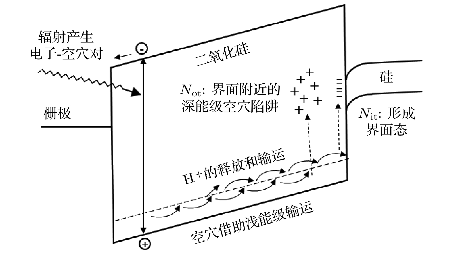
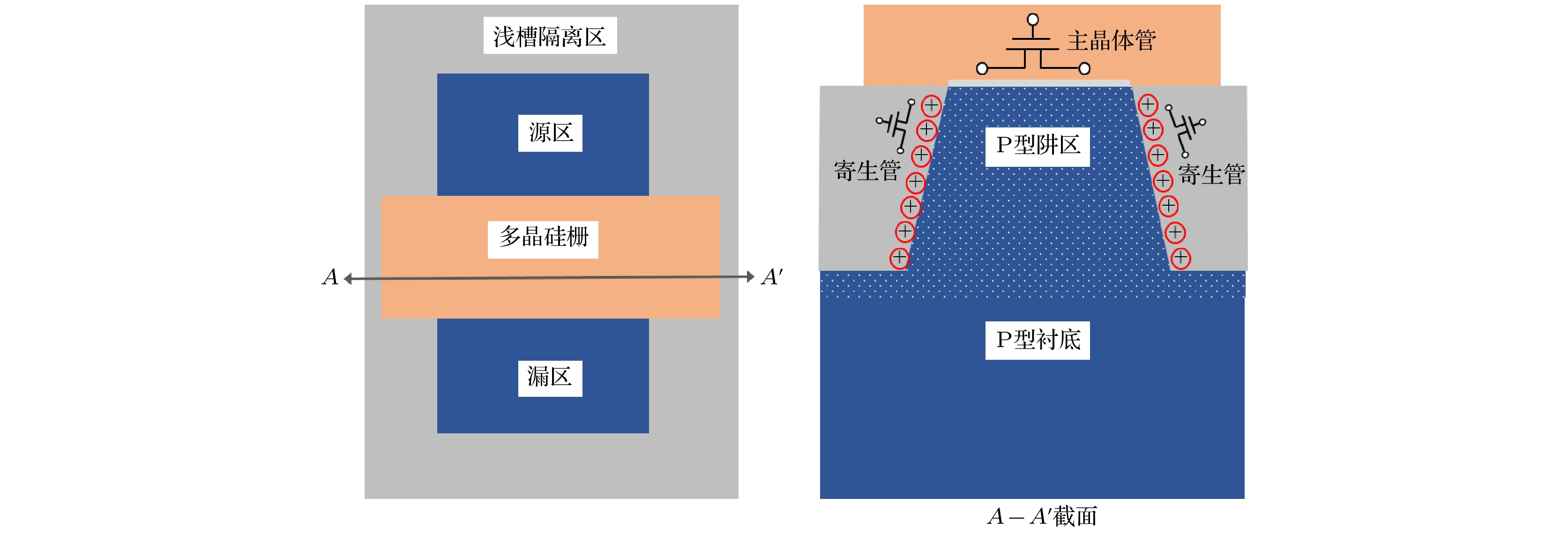
图 2 辐射导致的STI侧壁寄生NMOS示意图
Fig. 2. Schematic of radiation induced parasitic NMOS at STI sidewall.
图 3 传统的STI场区离子注入加固技术示意图 (a)器件版图; (b)工艺示意图
Fig. 3. Schematic of traditional ion implantation technology on STI field region: (a) Layout of the device; (b) diagram of the process
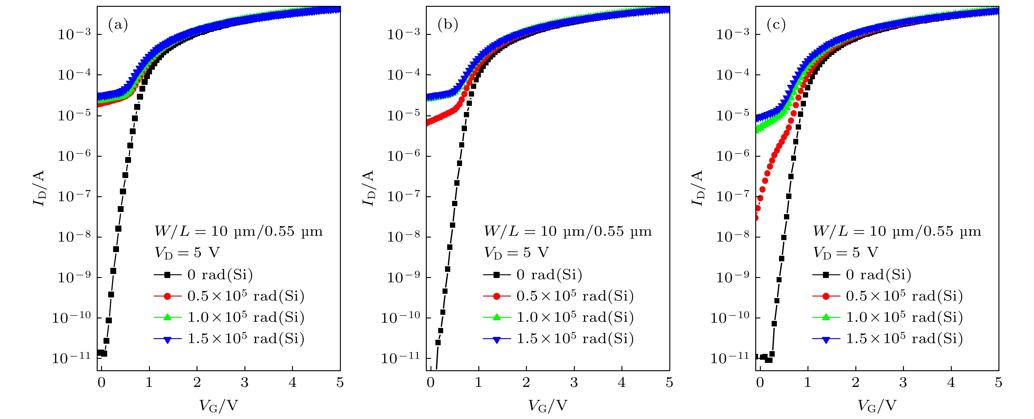
图 4 5 V NMOS器件总剂量效应测试结果 (a) 无STI场区离子注入; (b) 场区离子注入剂量5×1013 cm–2 ; (c) 场区离子注入剂量8×1013 cm–2
Fig. 4. Total ionizing dose test results of 5 V NMOS device: (a) Without STI field implantation; (b) STI filed implantation dose 5×1013 cm–2 ; (c) STI filed implantation dose 8×1013 cm–2.

图 5 STI边缘掺杂离子浓度仿真 (a) STI结构中离子浓度分布图; (b) 不同工艺热预算下不同位置的离子浓度分布对比
Fig. 5. Simulation of doping concentration at STI edge region: (a) Ion distribution of STI structure; (b) doping profile comparison at various positions under different thermal budget.
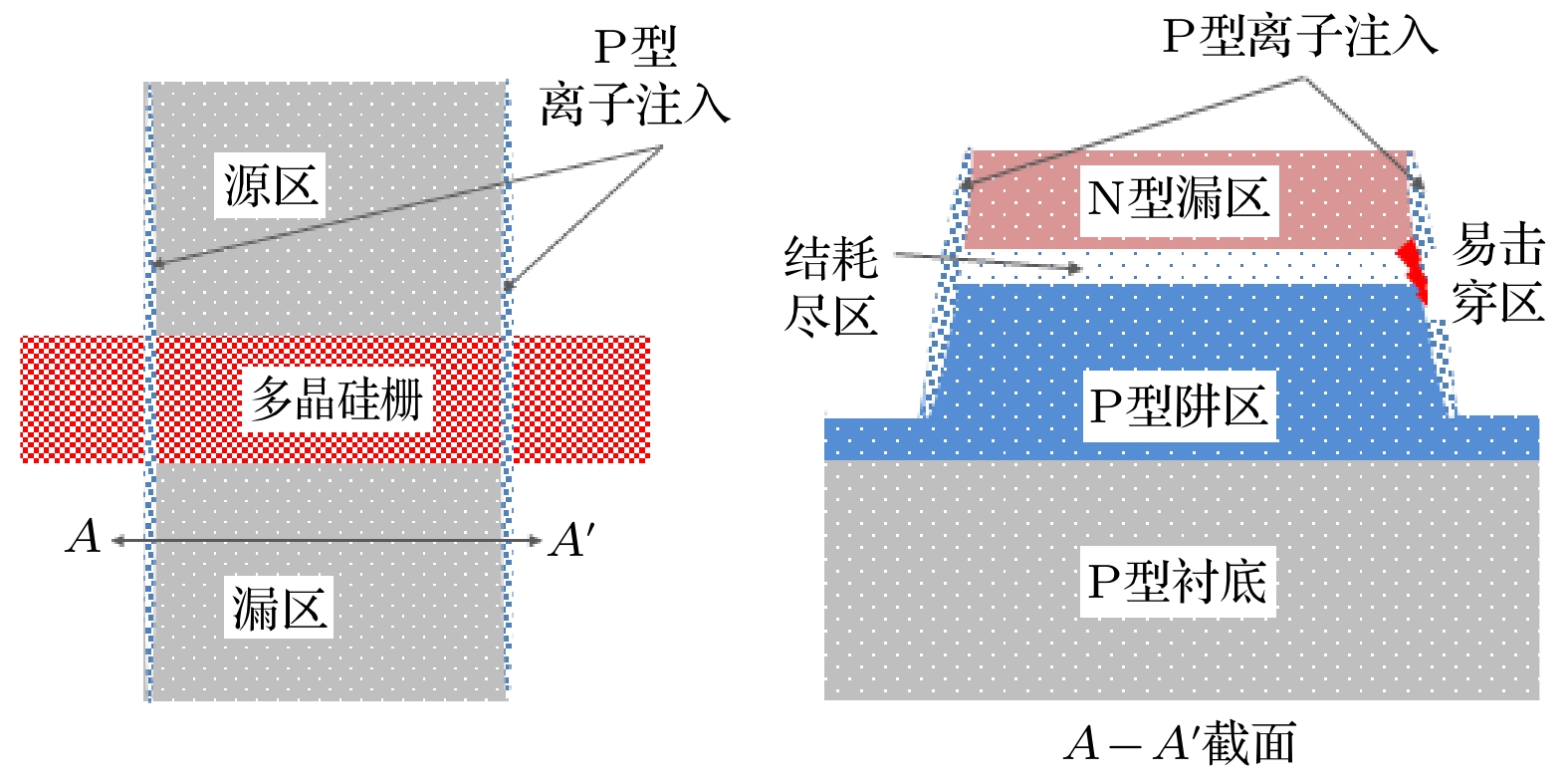
图 6 STI场区离子注入对漏击穿电压的影响示意图
Fig. 6. Schematic of the impact of ion implantation on drain breakdown voltage.
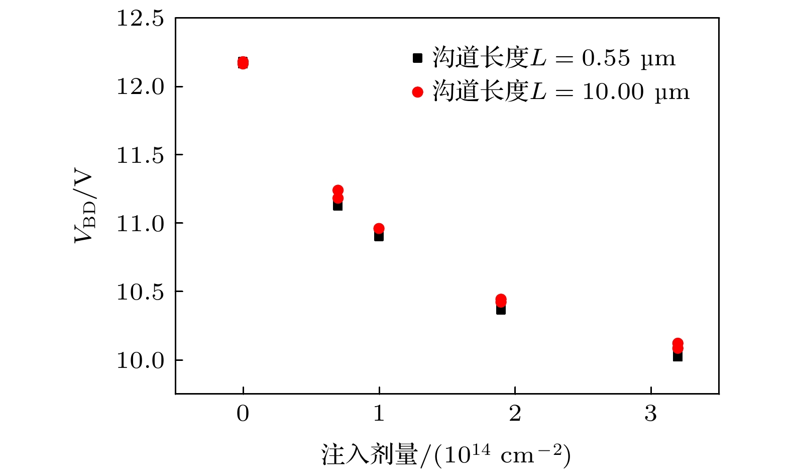
图 7 STI场区加固注入剂量对器件漏击穿电压的影响
Fig. 7. Impact of hardening implantation dose on drain breakdown voltage.
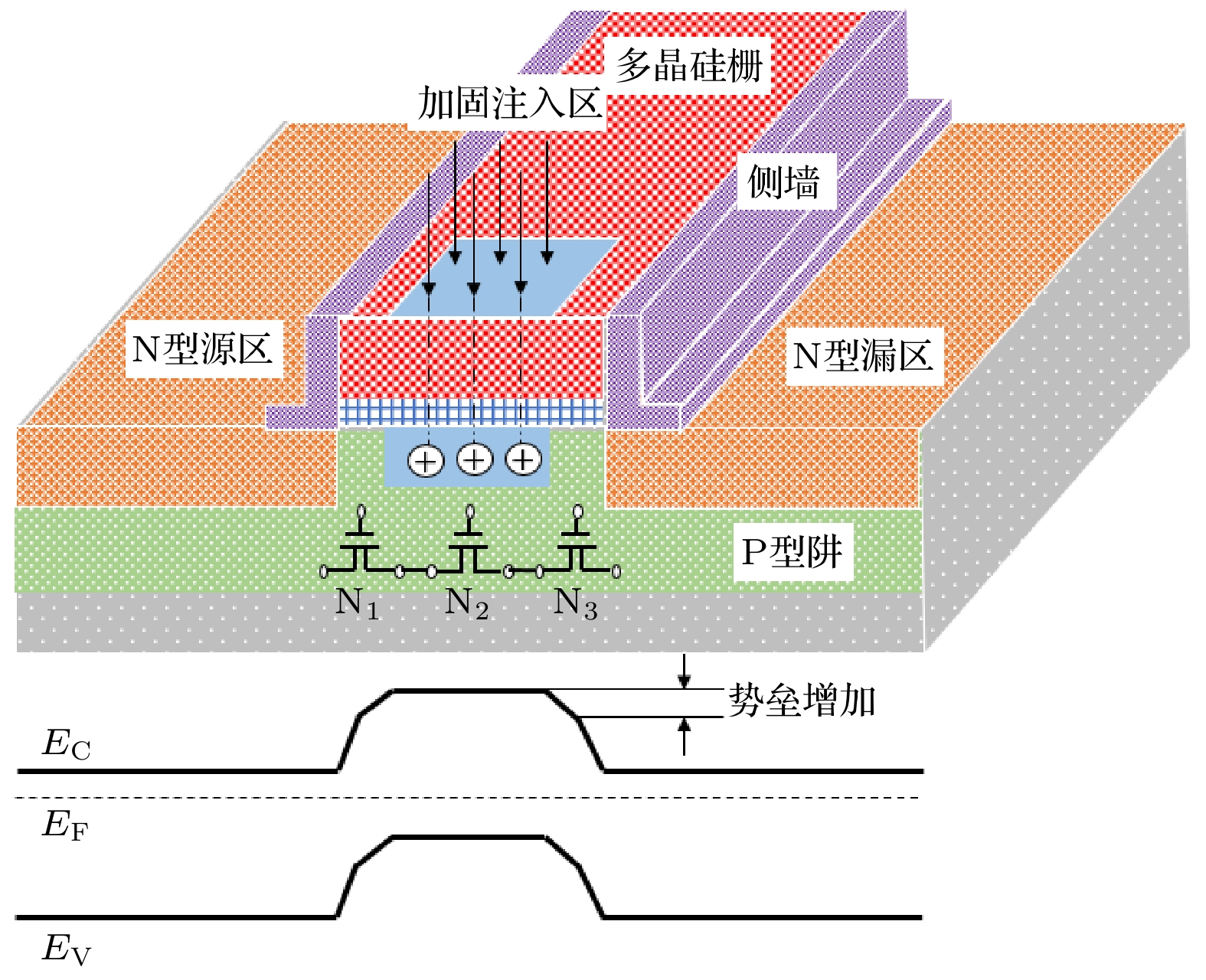
图 8 新型抗总剂量加固注入器件结构和能带图
Fig. 8. Device structure and band diagram with the new hardening ion implantation.

图 9 采用部分沟道离子注入器件总剂量效应 (a)加固注入剂量2×1013 cm–2; (b)加固注入剂5×1013 cm–2 ; (c)加固注入剂量8×1013 cm–2
Fig. 9. TID effect of the devices with partial channel hardened implantation: (a) Hardening implantation dose 2×1013 cm–2 ; (b) hardening implantation dose 5×1013 cm–2 ; (c) hardening implantation dose 8×1013 cm–2.
表 1 STI场区离子注入实验分片方案
Table 1. Split condition of ion implantation for experiment
样品 STI场区离子加固注入 能量/keV 剂量/cm–2 #1 120 0 #2 120 5×10¹³ #3 120 8×10¹³  下载: 导出CSV
表 2 两种注入加固方案测试结果对比
Table 2. Comparison of two total ionizing dose hardening methodology.
测试条件和参数 STI场区加固技术 部分沟道离子注入技术 #1 #2 #3 #4 #5 #6 辐照前 VT/V 0.72 0.75 0.78 0.74 0.76 0.79 IDsat/(μA·μm–1) 428 421 431 426 433 430 Ioff /(pA·μm–1) 9.7 9.5 1.4 2.0 1.1 2.2 BVD/V 12.2 11.4 11.1 12.1 12.2 12.1 1×10⁵ rad(Si)辐照后 VT/V NA NA 0.35 0.67 0.65 0.69 IDsat/(μA·μm–1) 448 436 445 444 449 441 Ioff /(pA·μm–1) 1.9×10⁷ 2.5×10⁷ 5.0×10⁶ 5.3×10² 5.9 3.0 辐照后
参数变化ΔVT/% — — –55.1 –9.5 –14.5 –12.7 ΔIDsat/% 4.7 3.6 3.2 4.2 3.7 2.6 ΔIoff/% 1.4×10⁸ 2.6×10⁸ 3.6×10⁸ 2.6×10⁵ 4.2×10² 36
下载: 导出CSV
-
[1] Barnaby H J, McLain M L, Sanchez Esqueda I, Chen X J 2009 IEEE Trans. Circuits Syst. Ⅰ 56 1870
Google Scholar
[2] 卓青青, 刘红侠, 杨兆年, 蔡慧民, 郝跃 2012 物理学报 61 220702
Google Scholar
Zhuo Q Q, Liu H X, Yang Z N, Cai H M, Hao Y 2012 Acta Phys. Sin. 61 220702
Google Scholar
[3] Zheng M Q, Liu Y, Duan C, Luo M T 2014 12 th IEEE International Conference on Solid-State and Integrated Circuit Technology Guilin, China, October 28–31, 2014 p1
[4] Liu Z L, Hu Z Y, Zhang Z X, Shao H, Chen M, Bi D W, Ning B X, Zou S C 2011 Microelectron. Reliab. 51 1148
Google Scholar
[5] Hu Z Y, Liu Z L, Shao H, Zhang Z X, Ning B X, Chen M, Bi D W, Zou S C 2011 Microelectron. Reliab. 51 1295
Google Scholar
[6] Liu Z L, Hu Z Y, Zhang Z X, Shao H, Chen M, Bi D W, Ning B X, Wang R, Zou S C 2010 Nucl. Instrum. Methods Phys. Res. Sect. B 268 3498
Google Scholar
[7] 刘一宁, 杨亚鹏, 陈法国, 张建岗, 郭荣, 梁润成 2021 核技术 44 030502
Google Scholar
Liu Y N, Yang Y P, Chen F G, Zhang J G, Guo R, Liang R C 2021 Nucl. Tech. 44 030502
Google Scholar
[8] Schwank J R, Shaneyfelt M R, Fleetwood D M, Felix J A, Dodd P E, Paillet P, VÉronique F C 2008 IEEE Trans. Nucl. Sci. 55 1833
Google Scholar
[9] Dodd P E, Shaneyfelt M R, Schwank J R, Felix 2010 IEEE Trans. Nucl. Sci. 57 1747
Google Scholar
[10] 王信, 陆妩, 吴雪, 马武英, 崔江维, 刘默寒, 姜柯 2014 物理学报 22 226101
Google Scholar
Wang X, Lu W, Wu X, Ma W Y, Cui J W, Liu M H, Jiang K 2014 Acta Phys. Sin. 22 226101
Google Scholar
[11] 郑齐文, 崔江维, 王汉宁, 周航, 余德昭, 魏莹, 苏丹丹 2016 物理学报 65 076102
Google Scholar
Zheng Q W, Cui J W, Wang H N, Zhou H, Yu D Z, Wei Y, Su D D 2016 Acta Phys. Sin. 65 076102
Google Scholar
[12] Giovanni B, Valentino L, Alberto S, Stefano G 2013 Proceedings of the European Conference on Radiation and its Effects on Components and Systems Oxford, UK, September 23–27, 2013 p1
[13] 范雪, 李威, 李平, 张斌, 谢小东, 王刚, 胡滨, 翟亚红 2012 物理学报 61 016106
Google Scholar
Fan X, Li W, Li P, Zhang B, Xie X D, Wang G, Hu B, Zhai Y H 2012 Acta Phys. Sin. 61 016106
Google Scholar
[14] Clark L T, Mohr K C, Holbert K E 2007 IEEE International Reliability Physics Symposium Proceedings Phoenix, USA, April 15–19, 2007 p582
[15] Lee M S, Lee H C 2013 IEEE Trans. Nucl. Sci. 60 3084
Google Scholar
[16] Malik M, Prakash N R, Kumar A, Jatana H S 2022 Silicon 14 3891
Google Scholar
[17] 董艺, 沈鸣杰, 刘岐 2018 航天器环境工程 35 468
Google Scholar
Dong Y, Shen M J, Liu Q 2018 Spacecr. Environ. Eng. 35 468
Google Scholar
[18] Chang J S, Chong K S, Shu W, Lin T, Jiang J, Lwin N K Z, Kang Y 2014 IEEE 57th International Midwest Symposium on Circuits and Systems College Station, USA, August 3–6, 2014 p821
[19] Vaz P I, Both T H, Vidor F F, Brum R M, Wirth G I 2018 J. Electron. Test. 34 735
Google Scholar
[20] Song L, Hu Z Y, Zhang M Y, Liu X N, Dai L H, Zhang Z X, Zou S C 2017 Microelectron. Reliab. 74 1
Google Scholar
[21] Peng C, Hu Z Y, En Y F, Chen Y Q, Lei Z F, Zhang Z G, Zhang Z X, Li B 2018 IEEE Trans. Nucl. Sci. 65 877
Google Scholar
[22] 谢儒彬, 吴建伟, 陈海波, 李艳艳, 洪根深 2016 太赫兹科学与电子信息学报 14 805
Google Scholar
Xie R B, Wu J W, Chen H B, Li Y Y, Hong G S 2016 J. Terahertz Sci. Electron. Inf. Technol. 14 805
Google Scholar
[23] 王思浩, 鲁庆, 王文华, 安霞, 黄如 2010 物理学报 59 1970
Google Scholar
Wang S H, Lu Q, Wang W H, An X, Huang R 2010 Acta Phys. Sin. 59 1970
Google Scholar

 下载:
下载:
计量
- 文章访问数: 8053
- PDF下载量: 82
- 被引次数: 0
