


-
ZnS作为一种宽带隙半导体, 以其优异的光电性能近年来受到广泛关注, 在太阳能电池、光催化剂以及传感器方面有着广阔的应用前景. 本文首先以射频磁控溅射方法沉积了ZnS薄膜, 然后在600 ℃温度和不同硫压下进行退火, 通过X射线衍射、扫描电子显微镜、能量散射X射线谱、紫外-可见透射光谱以及慢正电子多普勒展宽谱对ZnS薄膜的晶体结构、表面形貌、晶粒尺寸、成分、透光率以及缺陷进行分析. 结果表明: 硫气氛后退火能够改善ZnS薄膜结晶性, 退火后ZnS薄膜光学带隙为3.43—3.58 eV. 当硫压高于0.49 atm(1 atm = 1.01×10⁵ Pa)时, ZnS内部硫间隙原子以及表面单质硫降低了薄膜在可见光区的透光率. 慢正电子多普勒展宽谱结果还表明, ZnS薄膜的缺陷浓度由表层到内层逐渐降低, 薄膜缺陷随着硫压增加而降低. 同时, 3γ湮没证明了薄膜内部较为致密, 硫化会导致薄膜开孔率增加. 吸附硫通过内扩散占据了晶体中硫空位缺陷的位置, 导致缺陷浓度降低, 进而改善了薄膜质量.
-
关键词:
- 磁控溅射 /
- 硫蒸气退火 /
- ZnS薄膜 /
- 慢正电子多普勒展宽能谱
ZnS, a kind of wide-band gap semiconductor, has attracted extensive attention in recent years due to its excellent photoelectric performance, which has broad application prospects in solar cells, photocatalysts and sensors. In this work, ZnS thin films are first deposited by radio-frequency (RF) magnetron sputtering, and then annealed at 600 ℃ and different sulfur pressures. The crystal structure, surface morphology, grain size, composition, transmittance and defects of ZnS thin films are analyzed by X-ray diffraction, scanning electron microscopy, energy dispersive spectroscopy, UV-vis transmission spectra, and positron annihilation Doppler broadening spectroscopy. The results show that the crystallinities of ZnS films can be improved by being annealed in sulfur atmosphere, and the optical band gaps of ZnS films after being annealed are in a range of 3.43–3.58 eV. When the sulfur pressure is higher than 0.49 atm, the sulfur interstitial atoms in the ZnS and the elemental sulfur on the surface reduce the transmittance of the film in the visible region. The Doppler broadening spectroscopy results also show that the defect concentrations of ZnS films decrease gradually from their surface layers to the inner layers, and the defects of ZnS films decrease with the increase of sulfur pressure. Meanwhile, the 3γ annihilation also proves that the interior of the film is relatively dense, and the open porosity of the film will increase due to vulcanization. Adsorbed sulfur occupies the position of sulfur vacancy defect in the crystal through internal diffusion, which leads the defect concentration to decrease and the film quality to be improved.-
Keywords:
- magnetron sputtering /
- sulfidation annealing /
- ZnS thin films /
- positron annihilation Doppler broadening spectroscopy
[1] Liu C, Mu L, Jia J, Zhou X, Lin Y 2013 Electrochim. Acta 111 179
 Google Scholar
[2] Lin Y B, Lin Y, Meng Y, Wang Y 2014 Ceram. Int. 40 8157
Google Scholar
[3] Wang C, Li J, Feng W, Ye Y, Guo H 2021 Optik 242 167095
Google Scholar
[4] Le Donne A, Cavalcoli D, Mereu R A, Perani M, Pagani L, Acciarri M, Binetti S 2017 Mater Sci Semicond Process 71 7
Google Scholar
[5] Nayef U M 2017 Optik 130 441
Google Scholar
[6] Khan T M, Zakria M, Ahmad M, Shakoor R I 2014 J. Lumin. 147 97
Google Scholar
[7] Cheng Y C, Jin C Q, Gao F, Wu X L, Zhong W, Li S H, Chu P K 2009 J. Appl. Phys. 106 123101
Google Scholar
[8] Fang X S, Zhai T Y, Gautam U K, Li L, Wu L M, Yoshio B, Golberg D 2011 Prog. Mater. Sci. 56 175
Google Scholar
[9] Zapien J A, Jiang Y, Meng X M, Chen W, Au F C K, Lifshitz Y, Lee S T 2004 Appl. Phys. Lett. 84 1189
Google Scholar
[10] Cheng G, Hu D, Chen P, Duan Y, Zhao Y, Ma Y, Liu S 2012 Thin Solid Films 520 7153
Google Scholar
[11] Ummartyotin S, Infahsaeng Y 2016 Renew Sust. Energ. Rev. 55 17
Google Scholar
[12] Park S, Sun G J, Kim S, Lee S, Lee C 2015 Electron. Mater. Lett. 11 572
Google Scholar
[13] Thangavel S, Krishnamoorthy K, Kim S J, Venugopal G 2016 J. Alloys Compd. 683 456
Google Scholar
[14] Zhang R G, Wang B Y, Zhang H, Wei L 2005 Appl. Surf. Sci. 245 340
Google Scholar
[15] Lee G, Wu J J 2017 Powder Technol. 318 8
Google Scholar
[16] Shin S W, Kang S R, Yun J H, Moholkar A V, Moon J H, Lee J Y, Kim J H 2011 Sol. Energy Mater Sol. Cells 95 856
Google Scholar
[17] Karimi A, Sohrabi B, Vaezi M R 2018 Thin Solid Films 651 97
Google Scholar
[18] Ahmed A A, Eisa M H, Abdulla M D 2022 Chalcogenide Lett. 19 591
Google Scholar
[19] Amotchkina T, Trubetskov M, Hahner D, Pervak V 2020 Appl. Opt. 59 A40
Google Scholar
[20] Cui A, Sun C, Wang F, Ye Z 2021 Infrared. Phys. Technol. 114 103667
Google Scholar
[21] Liu W S, Huang C S, Chen S Y, Lee M Y, Kuo H C 2021 J. Alloys Compd. 884 161015
Google Scholar
[22] Ghosh P K, Jana S, Nandy S, Chattopadhyay K K 2007 Mater. Res. Bull. 42 505
Google Scholar
[23] Wang X, Shi J, Feng Z, Li M, Li C 2011 Phys. Chem. Chem. Phys. 13 4715
Google Scholar
[24] Miller A P 1941 Lange’s Handbook of Chemistry (4th Ed.) (Washington: Amer Public Health Assoc inc) p1324
[25] 曹兴忠, 宋力刚, 靳硕学, 张仁刚, 王宝义, 魏龙 2017 物理学报 66 29
Google Scholar
Cao X Z, Song L G, Jin S X, Zhang R G, Wang B Y, Wei L 2017 Acta Phys. Sin. 66 29
Google Scholar
[26] Imran M, Saleem A, Khan N A, Mehmood N 2018 Thin Solid Films 648 31
Google Scholar
[27] Bandic Z Z, Piquette E C, McCaldin J O, McGill T C 1998 Appl. Phys. Lett. 72 2862
Google Scholar
[28] Shan R, Yi J, Zhong J X, Yang S 2019 J. Mater. Sci. Mater. Electron. 30 13230
Google Scholar
[29] Chen S Z, Yu R S, Song L G, Zhang R G, Cao X Z, Wang B Y, Zhang P 2019 Appl. Surf. Sci. 498 143876
Google Scholar
[30] Tauc J, Grigorovici R, Vancu A 1966 Phys. Stat. Sol. 15 627
Google Scholar
[31] Hasaneen M F, Ali H M, Abd El-Raheem M M, Hakeem A M A 2020 Mater Sci. Eng. B 262 114704
Google Scholar
[32] Jubu P R, Yam F K, Igba V M, Beh K P 2020 J. Solid State Chem. 290 121576
Google Scholar
[33] Yu R S, Ito K, Hirata K, Zheng W, Kobayashi Y 2003 Appl. Phys. 6 3340
Google Scholar
[34] Wang B Y, Ma Y Y, Zhang Z, Yu R S, Wang P 2008 Appl. Surf. Sci. 255 119
Google Scholar
-

图 1 不同硫压条件下退火ZnS薄膜的XRD图
Fig. 1. XRD patterns of annealed ZnS films under different sulfur pressures.
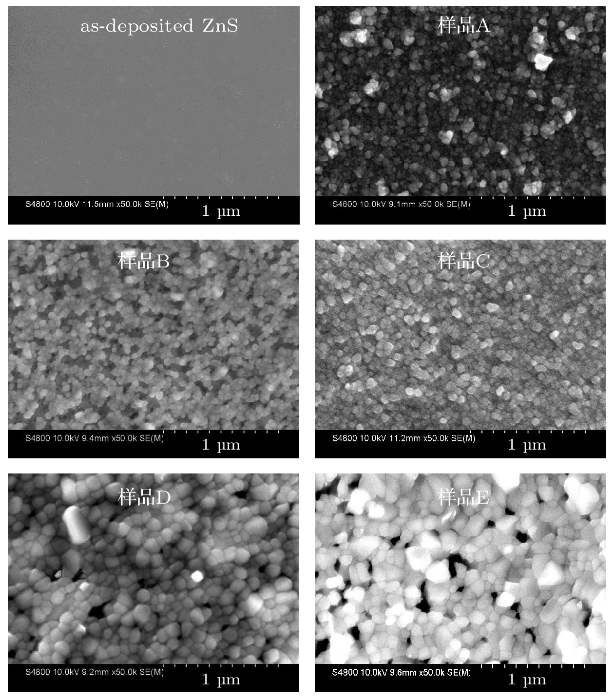
图 2 溅射沉积ZnS薄膜在硫蒸气中退火前后SEM图
Fig. 2. SEM images of sputter-deposited ZnS films before and after annealing in sulfur vapor.
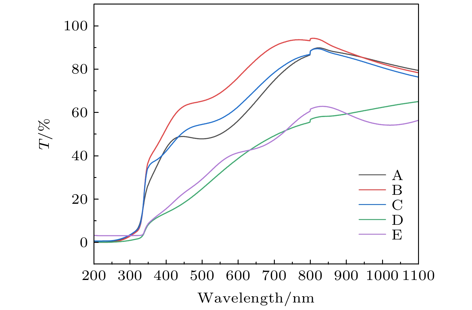
图 4 不同硫压条件下退火ZnS薄膜紫外-可见透射光谱
Fig. 4. UV-Vis transmission spectra of ZnS thin films annealed with different sulfur pressure.

图 5 不同硫压条件下退火ZnS薄膜的吸收系数
$ {\left(\alpha h\nu \right)}^{2} $ 与入射光子能量hν的关系曲线Fig. 5. Variation of
$ {\left(\alpha h\nu \right)}^{2} $ with hν for annealed ZnS films with different sulfur pressure.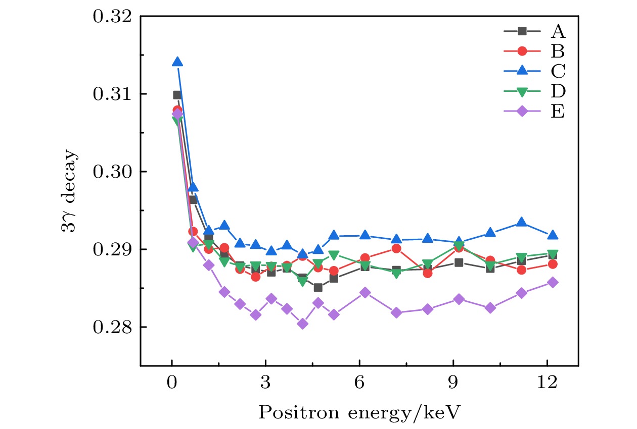
图 6 不同硫压条件下退火的ZnS薄膜3γ湮没图
Fig. 6. 3γ profiles as a function of positron implantation energy for ZnS films annealed with different sulfur pressure.
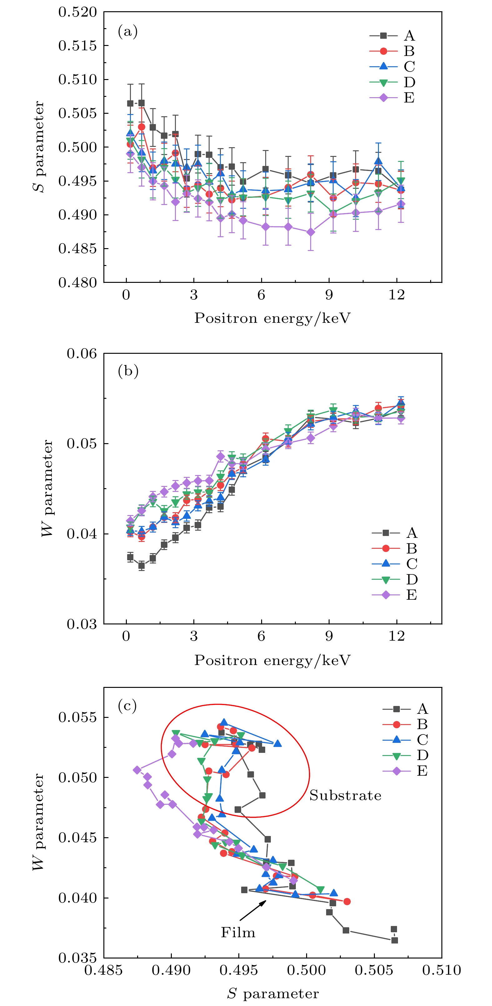
图 7 不同硫压条件下退火的ZnS薄膜的慢正电子DBS图 (a) E-S曲线; (b) E-W曲线; (c) S-W曲线
Fig. 7. Positron annihilation DBS of ZnS films annealed with different sulfur pressure: (a) E-S curves; (b) E-W curves; (c) S-W curves.
表 1 不同硫压下退火的ZnS薄膜(111)晶面的晶体参数
Table 1. Crystal parameters of (111) crystal planes of ZnS films annealed under the different sulfur pressures.
样品 晶面 FWHM 晶粒尺寸/nm A (111) 0.509 40.8 B (111) 0.344 60.4 C (111) 0.291 71.4 D (111) 0.209 99.4 E (111) 0.197 105.5  下载: 导出CSV
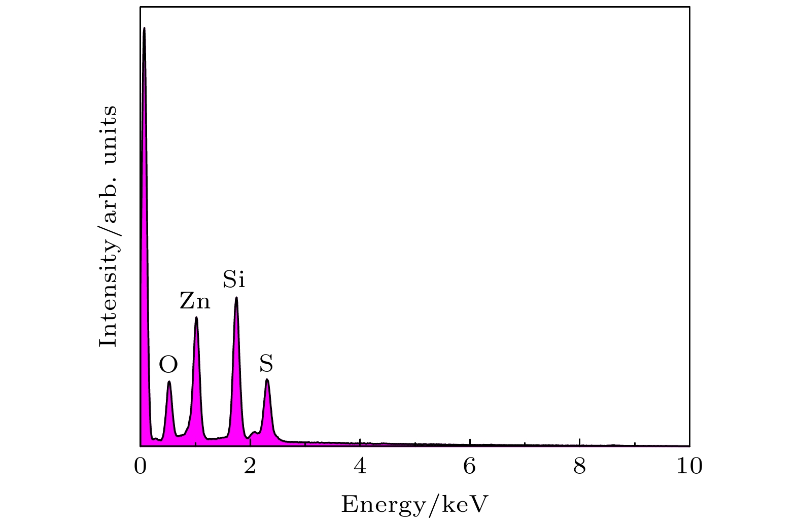
表 2 不同硫压条件下退火的ZnS样品的EDS测试结果
Table 2. EDS results of ZnS samples annealed under the different sulfur pressures.
样品 Zn S Zn/S A 17.53 18.77 0.94 B 19.42 18.67 1.04 C 19.25 18.63 1.03 D 16.17 15.09 1.07 E 32.43 31.61 1.03 as-deposited ZnS 21.27 5.81 3.66
下载: 导出CSV
-
[1] Liu C, Mu L, Jia J, Zhou X, Lin Y 2013 Electrochim. Acta 111 179
Google Scholar
[2] Lin Y B, Lin Y, Meng Y, Wang Y 2014 Ceram. Int. 40 8157
Google Scholar
[3] Wang C, Li J, Feng W, Ye Y, Guo H 2021 Optik 242 167095
Google Scholar
[4] Le Donne A, Cavalcoli D, Mereu R A, Perani M, Pagani L, Acciarri M, Binetti S 2017 Mater Sci Semicond Process 71 7
Google Scholar
[5] Nayef U M 2017 Optik 130 441
Google Scholar
[6] Khan T M, Zakria M, Ahmad M, Shakoor R I 2014 J. Lumin. 147 97
Google Scholar
[7] Cheng Y C, Jin C Q, Gao F, Wu X L, Zhong W, Li S H, Chu P K 2009 J. Appl. Phys. 106 123101
Google Scholar
[8] Fang X S, Zhai T Y, Gautam U K, Li L, Wu L M, Yoshio B, Golberg D 2011 Prog. Mater. Sci. 56 175
Google Scholar
[9] Zapien J A, Jiang Y, Meng X M, Chen W, Au F C K, Lifshitz Y, Lee S T 2004 Appl. Phys. Lett. 84 1189
Google Scholar
[10] Cheng G, Hu D, Chen P, Duan Y, Zhao Y, Ma Y, Liu S 2012 Thin Solid Films 520 7153
Google Scholar
[11] Ummartyotin S, Infahsaeng Y 2016 Renew Sust. Energ. Rev. 55 17
Google Scholar
[12] Park S, Sun G J, Kim S, Lee S, Lee C 2015 Electron. Mater. Lett. 11 572
Google Scholar
[13] Thangavel S, Krishnamoorthy K, Kim S J, Venugopal G 2016 J. Alloys Compd. 683 456
Google Scholar
[14] Zhang R G, Wang B Y, Zhang H, Wei L 2005 Appl. Surf. Sci. 245 340
Google Scholar
[15] Lee G, Wu J J 2017 Powder Technol. 318 8
Google Scholar
[16] Shin S W, Kang S R, Yun J H, Moholkar A V, Moon J H, Lee J Y, Kim J H 2011 Sol. Energy Mater Sol. Cells 95 856
Google Scholar
[17] Karimi A, Sohrabi B, Vaezi M R 2018 Thin Solid Films 651 97
Google Scholar
[18] Ahmed A A, Eisa M H, Abdulla M D 2022 Chalcogenide Lett. 19 591
Google Scholar
[19] Amotchkina T, Trubetskov M, Hahner D, Pervak V 2020 Appl. Opt. 59 A40
Google Scholar
[20] Cui A, Sun C, Wang F, Ye Z 2021 Infrared. Phys. Technol. 114 103667
Google Scholar
[21] Liu W S, Huang C S, Chen S Y, Lee M Y, Kuo H C 2021 J. Alloys Compd. 884 161015
Google Scholar
[22] Ghosh P K, Jana S, Nandy S, Chattopadhyay K K 2007 Mater. Res. Bull. 42 505
Google Scholar
[23] Wang X, Shi J, Feng Z, Li M, Li C 2011 Phys. Chem. Chem. Phys. 13 4715
Google Scholar
[24] Miller A P 1941 Lange’s Handbook of Chemistry (4th Ed.) (Washington: Amer Public Health Assoc inc) p1324
[25] 曹兴忠, 宋力刚, 靳硕学, 张仁刚, 王宝义, 魏龙 2017 物理学报 66 29
Google Scholar
Cao X Z, Song L G, Jin S X, Zhang R G, Wang B Y, Wei L 2017 Acta Phys. Sin. 66 29
Google Scholar
[26] Imran M, Saleem A, Khan N A, Mehmood N 2018 Thin Solid Films 648 31
Google Scholar
[27] Bandic Z Z, Piquette E C, McCaldin J O, McGill T C 1998 Appl. Phys. Lett. 72 2862
Google Scholar
[28] Shan R, Yi J, Zhong J X, Yang S 2019 J. Mater. Sci. Mater. Electron. 30 13230
Google Scholar
[29] Chen S Z, Yu R S, Song L G, Zhang R G, Cao X Z, Wang B Y, Zhang P 2019 Appl. Surf. Sci. 498 143876
Google Scholar
[30] Tauc J, Grigorovici R, Vancu A 1966 Phys. Stat. Sol. 15 627
Google Scholar
[31] Hasaneen M F, Ali H M, Abd El-Raheem M M, Hakeem A M A 2020 Mater Sci. Eng. B 262 114704
Google Scholar
[32] Jubu P R, Yam F K, Igba V M, Beh K P 2020 J. Solid State Chem. 290 121576
Google Scholar
[33] Yu R S, Ito K, Hirata K, Zheng W, Kobayashi Y 2003 Appl. Phys. 6 3340
Google Scholar
[34] Wang B Y, Ma Y Y, Zhang Z, Yu R S, Wang P 2008 Appl. Surf. Sci. 255 119
Google Scholar

 下载:
下载:


计量
- 文章访问数: 6591
- PDF下载量: 97
- 被引次数: 0
