


-
金属-半导体-金属(MSM)型氧化镓薄膜探测器的性能高度依赖于氧化镓薄膜的均匀性, 工艺难度较高, 对规模化、量产化薄膜探测器提出了挑战. 本文首次在量产化悬臂式薄膜芯片表面物理沉积氧化镓薄膜, 实现了一个五对叉指电极结构的MSM型氧化镓薄膜日盲探测器. 得益于微机电系统(MEMS)工艺制备的悬臂式电极结构保护了内部电路与探测薄膜的完整均匀性, 所获得的氧化镓薄膜虽然是非晶结构, 但探测器仍然具备良好的紫外探测性能. 在18 V偏压下其探测率达到7.9×10¹⁰ Jones, 外量子效率达到1779%, 上升和下降时间分别为1.22 s和0.24 s, 接近晶体氧化镓薄膜的探测性能. 该探测器在无任何光学聚焦系统的情况下, 实现了对户外日光环境下脉冲电弧的灵敏检测, 将在日盲探测领域具有良好的潜在应用价值. 本工作基于MEMS工艺的悬臂式电极结构开发的敏感功能薄膜沉积技术, 避免了功能薄膜大面积均匀性对刻蚀电路的影响, 为MSM型薄膜探测器的制备提供了新的技术方法和工艺路线.The performance of gallium oxide (Ga2O3) thin film detector based on metal-semiconductor-metal (MSM) is highly dependent on the uniformity of the Ga2O3 thin film, and the manufacturing process is quite sophisticated, which poses a challenge for the scale-up and mass production of thin film photodetectors. In this work, an MSM Ga2O3 thin film solar-blind photodetector with five-finger interdigital electrodes is fabricated by physically depositing Ga2O3 thin film on the surface of a mass-produced cantilevered thin film chip. Through the microelectromechanical system (MEMS) process, the cantilever electrode structure is prepared, which protects the internal circuit and the integrity of the thin film. The Ga2O3 thin film treated by argon plasma at a low temperature is amorphous, but the photodetector still possesses considerable ultraviolet detection performance. At a bias voltage of 18 V, it approaches the detection performance of crystalline Ga2O3 thin film, with a detectivity of 7.9×10¹⁰ Jones, an external quantum efficiency of 1779%, rise time and decay time of 1.22 s and 0.24 s, respectively. Moreover, a system of arc detection is built in outdoor environments. Without any optical focusing system, this photodetector achieves sensitive detection of pulsed arc in an outdoor sunlight environments. For pulsed arcs with an output voltage of 100 kV, the photodetector is capable of sensitive detection at a distance of 25 cm. Besides, the maximum detection distance of 155 cm indicates that the photodetector will have a favorable potential application value in the field of solar-blind detection. This work develops a sensitive functional thin film deposition technology based on the cantilever electrode structure fabricated by the MEMS process, which avoids the influence of the large-area uniformity of the functional thin film on the etching circuit. It provides a new technical approach and process route for preparing MSM photodetectors.
-
Keywords:
- gallium oxide /
- solar-blind photodetector /
- arc detection
[1] Xie C, Lu X T, Tong X W, Zhang Z X, Liang F X, Liang L, Luo L B, Wu Y C 2019 Adv. Funct. Mater. 29 1806006
 Google Scholar
[2] Wu Z P, Jiao L, Wang X L, Guo D Y, Li W H, Li L H, Huang F, Tang W H 2017 J. Mater. Chem. C 5 8688
Google Scholar
[3] Chen M X, Zhao B, Hu G F, Fang X S, Wang H, Wang L, Luo J, Han X, Wang X D, Pan C F, Wang Z L 2018 Adv. Funct. Mater. 28 1706379
Google Scholar
[4] Sheoran H, Kumar V, Singh R 2022 ACS Appl. Electron. Mater. 4 2589
Google Scholar
[5] Yan Z Y, Li S, Liu Z, Zhi Y S, Dai J, Sun X Y, Sun S Y, Guo D Y, Wang X, Li P G, Wu Z P, Li L L, Tang W H 2020 J. Mater. Chem. C 8 4502
Google Scholar
[6] Yan Z Y, Li S, Liu Z, Liu W J, Qiao F, Li P G, Tang X, Li X H, Yue J Y, Guo Y F, Tang W H 2022 IEEE J. Sel. Top. Quantum Electron. 28 3803208
Google Scholar
[7] Liu Z, Li S, Yan Z Y, Liu Y Y, Zhi Y S, Wang X, Wu Z P, Li P G, Tang W H 2020 J. Mater. Chem. C 8 5071
Google Scholar
[8] Yan Z Y, Li S, Yue J Y, Liu Z, Ji X Q, Yang Y, Li P G, Wu Z P, Guo Y, Tang W H 2021 ACS Appl. Mater. Interfaces 13 57619
Google Scholar
[9] Li S, Guo D Y, Li P G, Wang X, Wang Y, Yan Z Y, Liu Z, Zhi Y S, Huang Y, Wu Z P, Tang W H 2019 ACS Appl. Mater. Interfaces 11 35105
Google Scholar
[10] Li S, Zhi Y S, Lu C, Wu C, Yan Z Y, Liu Z, Yang J, Chu X, Guo D Y, Li P G, Wu Z P, Tang W H 2021 J. Phys. Chem. Lett. 12 447
Google Scholar
[11] Fu S, Wang Y, Gao C, Han Y, Fu R, Wang L, Li B, Ma J, Fu Z, Xu H, Liu Y 2023 IEEE Electron Device Lett. 44 1428
Google Scholar
[12] Li X, Xu F, Wang X, Luo J, Ding K, Ye L, Li H, Xiong Y, Yu P, Kong C, Ye L, Zhang H, Li W 2023 Phys. Status Solidi RRL DOI:10.1002/pssr.202200512
[13] 王江, 罗林保 2021 中国激光 48 7
Google Scholar
Wang J, Luo L B 2021 Chin. J. Lasers 48 7
Google Scholar
[14] Gao C, Wang Y, Fu S, Xia D, Han Y, Ma J, Xu H, Li B, Shen A, Liu Y 2023 ACS Appl. Mater. Interfaces 15 38612
Google Scholar
[15] 刘增, 李磊, 支钰崧, 都灵, 方君鹏, 李山, 余建刚, 张茂林, 杨莉莉, 张少辉, 郭宇锋, 唐为华 2022 物理学报 71 208501
Google Scholar
Liu Z, Li L, Zhi Y S, Du L, Fang J P, Li S, Yu J G, Zhang M L, Yang L L, Zhang S H, Guo Y F, Tang W H 2022 Acta Phys. Sin. 71 208501
Google Scholar
[16] Ni S, Chen Q, Liu J, Yang S, Li T, Yang X, Zhao J 2019 J. Power Sources 433 126681
Google Scholar
[17] Prabakar K, Venkatachalam S, Jeyachandran Y L, Narayandass S K, Mangalaraj D 2004 Mater. Sci. Eng. B 107 99
Google Scholar
[18] Onuma T, Saito S, Sasaki K, Masui T, Yamaguchi T, Honda T, Higashiwaki M 2015 Jpn. J. Appl. Phys. 54 112601
Google Scholar
[19] Li S, Yue J Y, Ji X Q, Lu C, Yan Z Y, Li P G, Guo D Y, Wu Z P, Tang W H 2021 J. Mater. Chem. C 9 5437
Google Scholar
[20] Chen Y C, Lu Y J, Liao M Y, Tian Y Z, Liu Q, Gao C J, Yang X, Shan C X 2019 Adv. Funct. Mater. 29 1906040
Google Scholar
[21] Chen Y C, Lu Y J, Liu Q, Lin C N, Guo J, Zang J H, Tian Y Z, Shan C X 2019 J. Mater. Chem. C 7 2557
Google Scholar
[22] Zhi Y S, Liu Z, Zhang S H, Li S, Yan Z Y, Li P G, Tang W H 2021 IEEE Trans. Electron Devices 68 3435
Google Scholar
[23] Lu Y C, Zhang Z F, Yang X, He G H, Lin C N, Chen X X, Zang J H, Zhao W B, Chen Y C, Zhang L L, Li Y Z, Shan C X 2022 Nano Res. 15 7631
Google Scholar
[24] Pearton S J, Yang J, Cary P H, Ren F, Kim J, Tadjer M J, Mastro M A 2018 Appl. Phys. Rev. 5 011301
Google Scholar
[25] Yang C, Liang H, Zhang Z, Xia X, Tao P, Chen Y, Zhang H, Shen R, Luo Y, Du G 2018 RSC Adv. 8 6341
Google Scholar
[26] Arora K, Goel N, Kumar M, Kumar M 2018 ACS Photonics 5 2391
Google Scholar
[27] Sun P, Yang X, Li K, Wei Z, Fan W, Wang S, Zhou W, Shan C 2023 Adv. Mater. Interfaces DOI: 10.1002/admi.202300371
[28] Xu R, Ma X, Chen Y, Mei Y, Ying L, Zhang B, Long H 2022 Mater. Sci. Semicond. Process. 144 106621
Google Scholar
[29] He M, Zeng Q, Ye L 2023 Crystals 13 1434
Google Scholar
[30] Zhang C, Liu K, Ai Q, Huang X, Chen X, Zhu Y, Yang J, Cheng Z, Li B, Liu L, Shen D 2022 J. Phys. Chem. C 126 21839
Google Scholar
[31] Kufer D, Nikitskiy I, Lasanta T, Navickaite G, Koppens F H, Konstantatos G 2015 Adv. Mater. 27 176
Google Scholar
[32] 况丹, 徐爽, 史大为, 郭建, 喻志农 2023 物理学报 72 038501
Google Scholar
Kuang D, Xu S, Shi D W, Guo J, Yu Z N 2023 Acta Phys. Sin. 72 038501
Google Scholar
[33] Yu J, Lou J, Wang Z, Ji S, Chen J, Yu M, Peng B, Hu Y, Yuan L, Zhang Y, Jia R 2021 J. Alloys Compd. 872 159508
Google Scholar
[34] Gu K Y, Zhang Z L, Huang H F, Tang K, Huang J, Liao M Y, Wang L J 2023 J. Mater. Chem. C 11 5371
Google Scholar
[35] 落巨鑫, 高红丽, 邓金祥, 任家辉, 张庆, 李瑞东, 孟雪 2023 物理学报 72 028502
Google Scholar
Luo J X, Gao H L, Deng J X, Ren J H, Zhang Q, Li R D, Meng X 2023 Acta Phys. Sin. 72 028502
Google Scholar
[36] Xi Z Y, Yang L L, Shu L C, Zhang M L, Li S, Shi L, Liu Z, Guo Y F, Tang W H 2023 Chin. Phys. B 32 088502
Google Scholar
[37] Wang J, Xiong Y, Ye L, Li W, Qin G, Ruan H, Zhang H, Fang L, Kong C, Li H 2021 Opt. Mater. 112 110808
Google Scholar
[38] Ren Q, Xu W, Shen Z, You T, Liu Q, Liu C, Zhao L, Chen L, Yu W 2020 ACS Appl. Electron. Mater. 3 451
Google Scholar
[39] Almaev A, Nikolaev V, Kopyev V, Shapenkov S, Yakovlev N, Kushnarev B, Pechnikov A, Deng J, Izaak T, Chikiryaka À, Scheglov M, Zarichny A 2023 IEEE Sens. J. 23 19245
Google Scholar
[40] Zhang M, Ma W, Li S, Yang L, Liu Z, Guo Y, Tang W H 2023 IEEE Trans. Electron Devices 70 2336
Google Scholar
[41] Liu Z, Zhi Y S, Zhang M L, Yang L L, Li S, Yan Z Y, Zhang S H, Guo D Y, Li P G, Guo Y F, Tang W H 2022 Chin. Phys. B 31 088503
Google Scholar
-
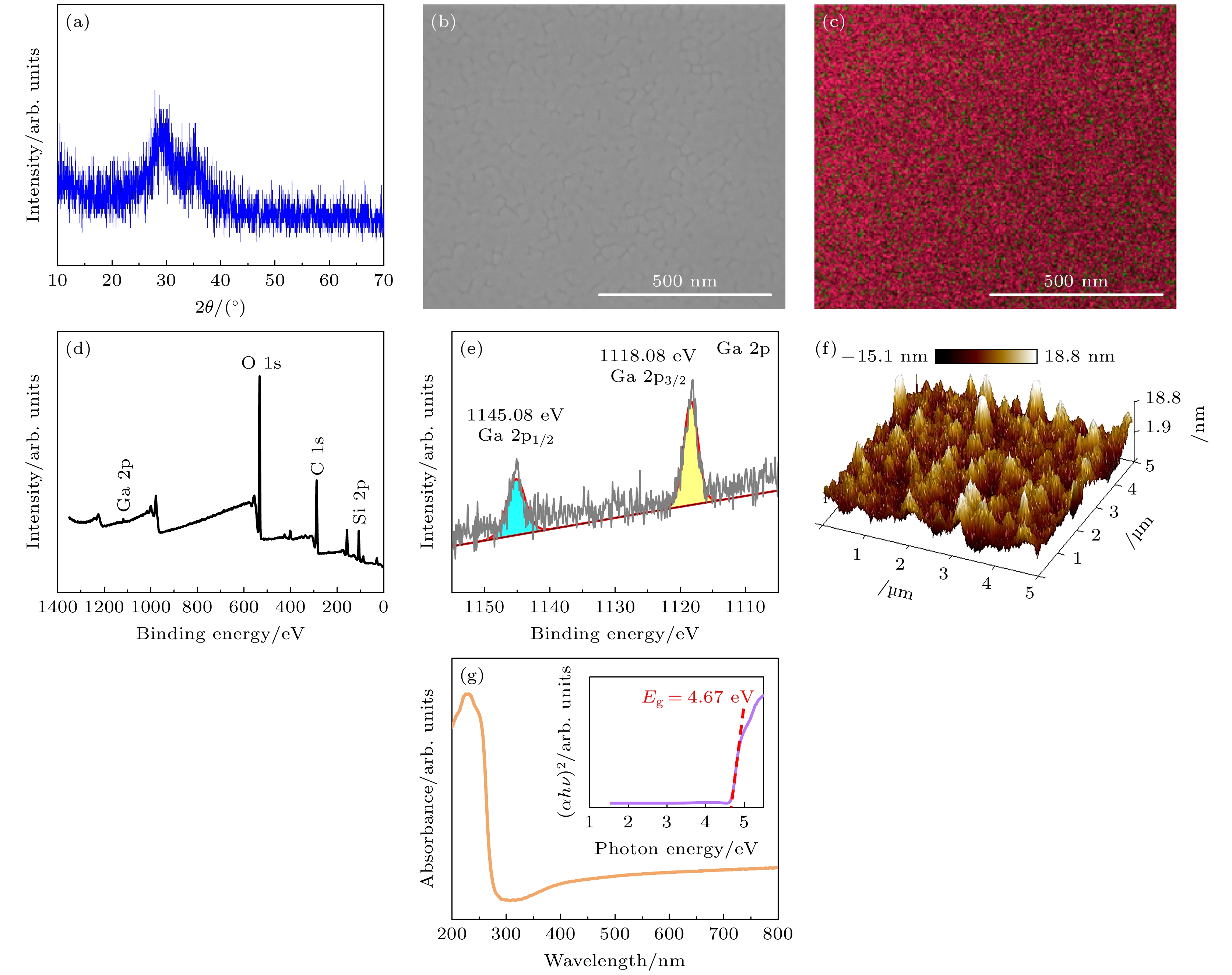
图 1 Ga2O3薄膜的(a) XRD图谱、(b) SEM图像、(c) EDS图谱、(d) XPS能谱、(e) Ga 2p能谱、(f) AFM图谱和(g) 光吸收曲线; 图(g)插图显示了$ (\alpha h\nu {)}^{2} $与$ h\nu $的光学带隙图.
Fig. 1. (a) XRD pattern, (b) SEM image, (c) EDS pattern, (d) XPS energy spectrum, (e) Ga 2p spectrum, (f) AFM pattern, (g) optical absorption curve of Ga2O3 thin film. The inset in panel (g) shows the curve of $ (\alpha h\nu {)}^{2} $ versus $ h\nu $ for the determination of the optical band gap of Ga2O3 thin film.
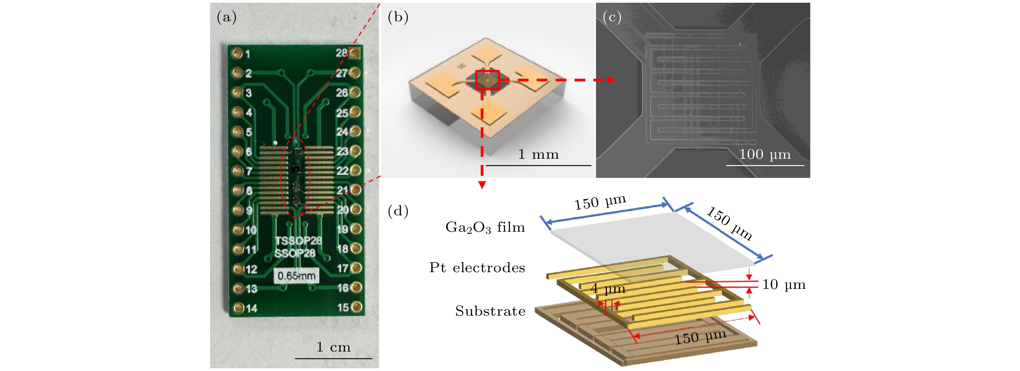
图 2 (a) Ga2O3薄膜探测器的实物照片; (b) 悬臂式薄膜芯片的结构示意图; (c) 图(b)红色框中的叉指电极SEM图像; (d) 图(b)红色框中叉指电极的详细结构示意图
Fig. 2. (a) Physical photograph of Ga2O3 thin film-based photodetector; (b) schematic of the structure of the cantilevered thin film chip; (c) the SEM image of interdigital electrodes in the red box in panel (b); (d) the detailed schematic structure of interdigital electrodes in the red box in panel (b).
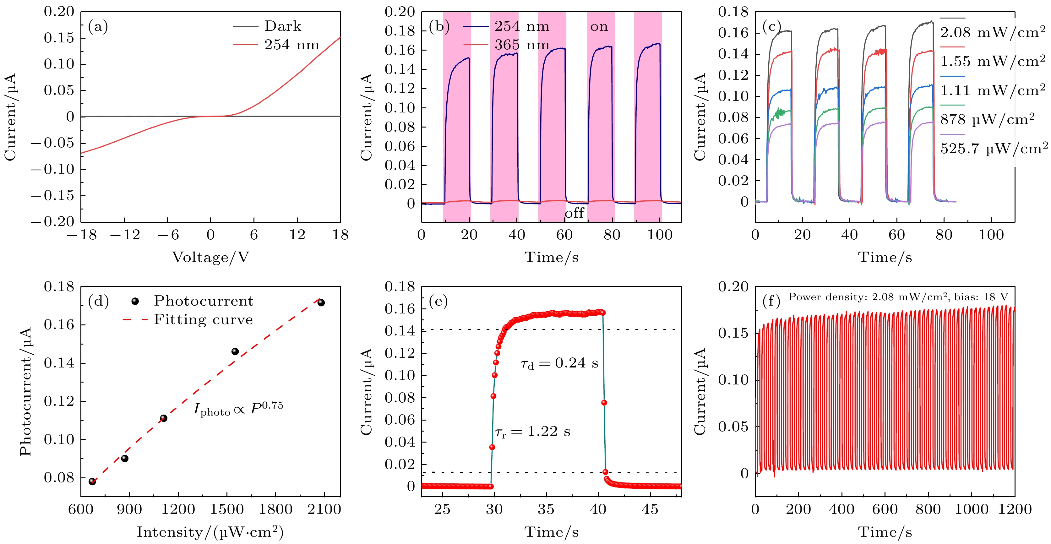
图 3 Ga2O3薄膜探测器 (a) 在黑暗和254 nm光照下的I-V曲线; (b) 254 nm和365 nm光照下的动态响应曲线; (c) 在18 V偏压下不同光照强度的动态响应曲线; (d) 光电流与光强的关系; (e) 上升/下降曲线; (f) 数十个操作周期切换
Fig. 3. Ga2O3 thin film detector: (a) I-V curves of the photodetector in the dark and under 254 nm illumination; (b) I-t curves operated at 254 nm and 365 nm illumination (2.08 mW/cm2); (c) I-t curves of the photodetector under different light intensities of 254 nm with a bias voltage of 18 V; (d) photocurrent versus light intensity; (e) rise/decay curves; (f) over tens of operation cycles.
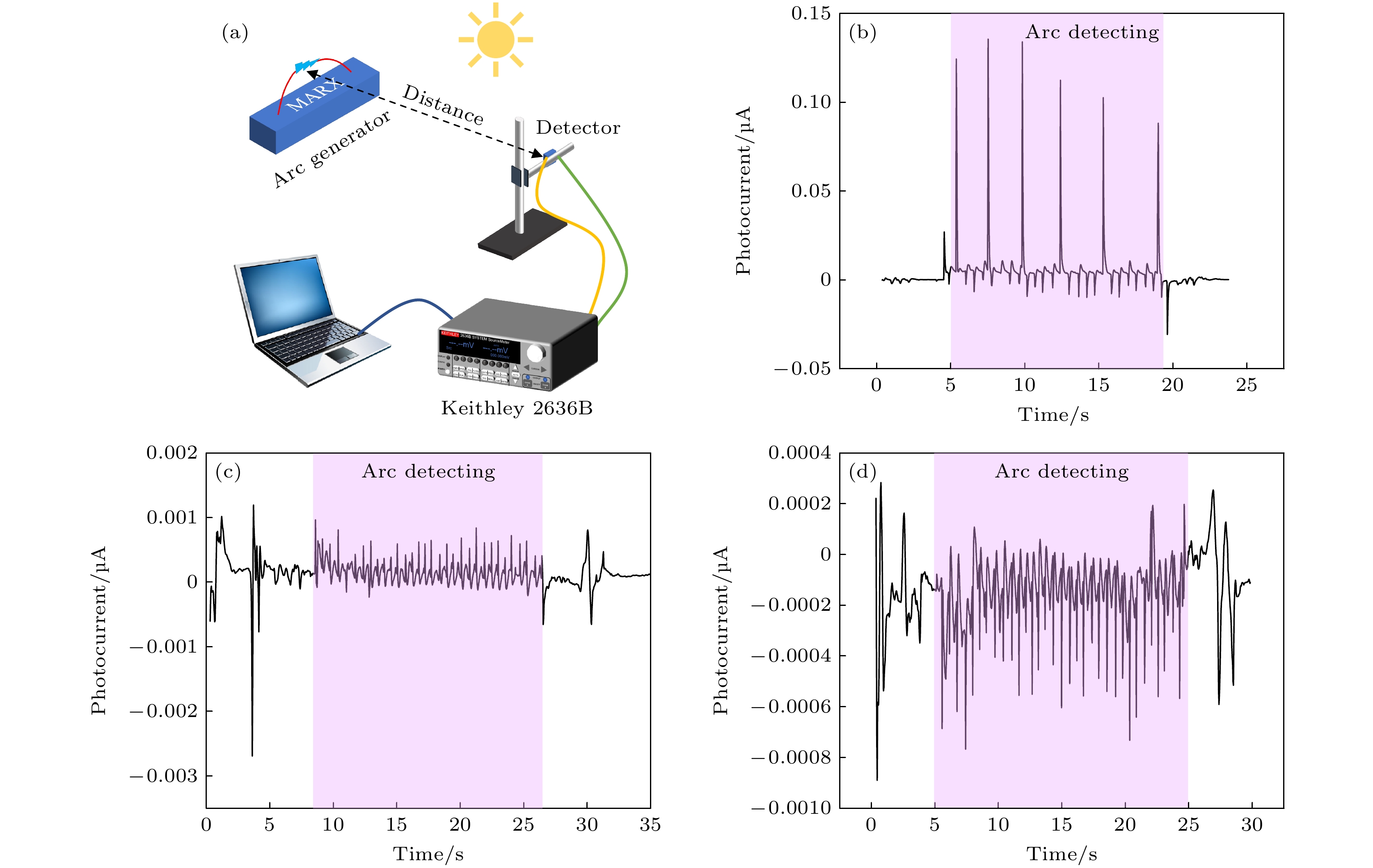
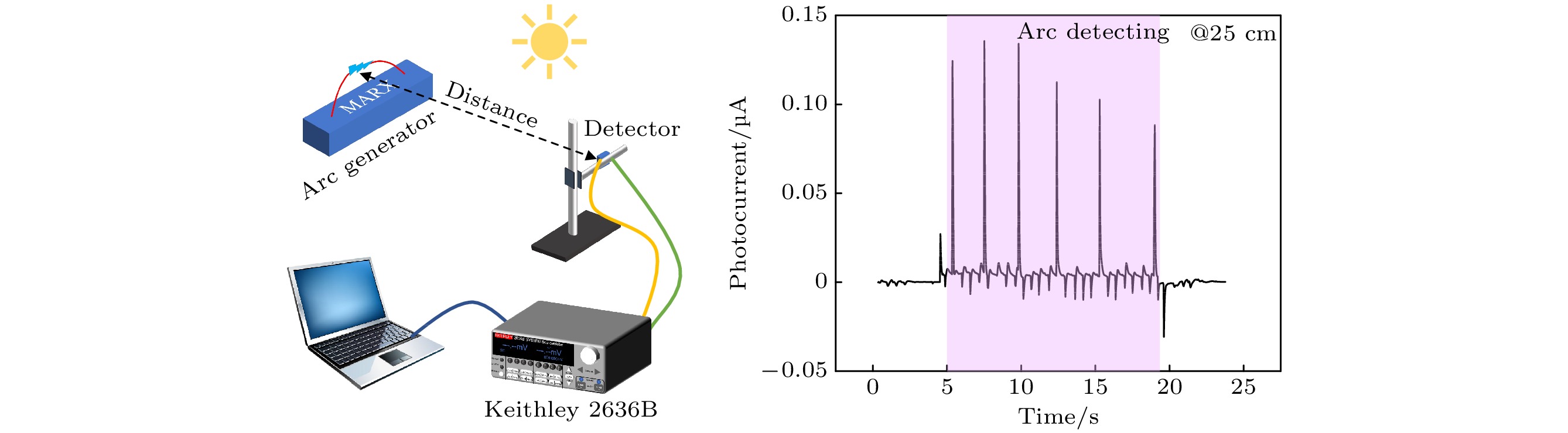
图 4 (a) 户外电弧检测系统; 电弧与探测器距离(b) 25 cm, (c) 155 cm, (d) 165 cm的响应曲线
Fig. 4. (a) Outdoor arc detection system; response curves for the arc to detector distances of (b) 25 cm, (c) 155 cm and (d) 165 cm.
表 1 MSM型Ga2O3薄膜光电探测器的光响应参数比较
Table 1. Comparison of photoresponse parameters of MSM type photodetectors based on Ga2O3 thin film.
制备方法 偏压/V 暗电流/nA PDCR R/(A·W–1) D*/Jones EQE/% $ {\tau }_{{\mathrm{r}}}/ $s $ {\tau }_{{\mathrm{d}}} $/s Ref. MOCVD、磁控溅射 10 0.17 3.5$ \times $103 9.4 1.17$ \times $1012 4.6$ \times $103 27 3.93 [28] 离子切割、光刻工艺 10 0.0287 953 0.13 — — 2.96/34.17 1.94/32.64 [38] 脉冲激光沉积、磁控溅射 –15 12.4 — 29.08 2.16$ \times $1011 1.4$ \times $104 0.41/0.52 1.06/1.68 [33] 卤化物气相外延、
真空沉积和光刻工艺10 10–2 — 7$ \times $104 1.12$ \times $1018 3.79$ \times $105 — — [39] MOCVD、磁控溅射 5 $ < $10–3 1.1$ \times $106 0.046 3.4$ \times $1013 22.4 0.96 0.19 [40] MOCVD、光刻和离子束溅射 10 1.9$ \times $10–3 8.97$ \times $107 634.15 5.93$ \times $1011 3.1$ \times $105 — — [41] MEMS工艺、磁控溅射 18 1.3 130 0.364 7.9$ \times $1010 1779 1.22 0.24 This work  下载: 导出CSV
-
[1] Xie C, Lu X T, Tong X W, Zhang Z X, Liang F X, Liang L, Luo L B, Wu Y C 2019 Adv. Funct. Mater. 29 1806006
Google Scholar
[2] Wu Z P, Jiao L, Wang X L, Guo D Y, Li W H, Li L H, Huang F, Tang W H 2017 J. Mater. Chem. C 5 8688
Google Scholar
[3] Chen M X, Zhao B, Hu G F, Fang X S, Wang H, Wang L, Luo J, Han X, Wang X D, Pan C F, Wang Z L 2018 Adv. Funct. Mater. 28 1706379
Google Scholar
[4] Sheoran H, Kumar V, Singh R 2022 ACS Appl. Electron. Mater. 4 2589
Google Scholar
[5] Yan Z Y, Li S, Liu Z, Zhi Y S, Dai J, Sun X Y, Sun S Y, Guo D Y, Wang X, Li P G, Wu Z P, Li L L, Tang W H 2020 J. Mater. Chem. C 8 4502
Google Scholar
[6] Yan Z Y, Li S, Liu Z, Liu W J, Qiao F, Li P G, Tang X, Li X H, Yue J Y, Guo Y F, Tang W H 2022 IEEE J. Sel. Top. Quantum Electron. 28 3803208
Google Scholar
[7] Liu Z, Li S, Yan Z Y, Liu Y Y, Zhi Y S, Wang X, Wu Z P, Li P G, Tang W H 2020 J. Mater. Chem. C 8 5071
Google Scholar
[8] Yan Z Y, Li S, Yue J Y, Liu Z, Ji X Q, Yang Y, Li P G, Wu Z P, Guo Y, Tang W H 2021 ACS Appl. Mater. Interfaces 13 57619
Google Scholar
[9] Li S, Guo D Y, Li P G, Wang X, Wang Y, Yan Z Y, Liu Z, Zhi Y S, Huang Y, Wu Z P, Tang W H 2019 ACS Appl. Mater. Interfaces 11 35105
Google Scholar
[10] Li S, Zhi Y S, Lu C, Wu C, Yan Z Y, Liu Z, Yang J, Chu X, Guo D Y, Li P G, Wu Z P, Tang W H 2021 J. Phys. Chem. Lett. 12 447
Google Scholar
[11] Fu S, Wang Y, Gao C, Han Y, Fu R, Wang L, Li B, Ma J, Fu Z, Xu H, Liu Y 2023 IEEE Electron Device Lett. 44 1428
Google Scholar
[12] Li X, Xu F, Wang X, Luo J, Ding K, Ye L, Li H, Xiong Y, Yu P, Kong C, Ye L, Zhang H, Li W 2023 Phys. Status Solidi RRL DOI:10.1002/pssr.202200512
[13] 王江, 罗林保 2021 中国激光 48 7
Google Scholar
Wang J, Luo L B 2021 Chin. J. Lasers 48 7
Google Scholar
[14] Gao C, Wang Y, Fu S, Xia D, Han Y, Ma J, Xu H, Li B, Shen A, Liu Y 2023 ACS Appl. Mater. Interfaces 15 38612
Google Scholar
[15] 刘增, 李磊, 支钰崧, 都灵, 方君鹏, 李山, 余建刚, 张茂林, 杨莉莉, 张少辉, 郭宇锋, 唐为华 2022 物理学报 71 208501
Google Scholar
Liu Z, Li L, Zhi Y S, Du L, Fang J P, Li S, Yu J G, Zhang M L, Yang L L, Zhang S H, Guo Y F, Tang W H 2022 Acta Phys. Sin. 71 208501
Google Scholar
[16] Ni S, Chen Q, Liu J, Yang S, Li T, Yang X, Zhao J 2019 J. Power Sources 433 126681
Google Scholar
[17] Prabakar K, Venkatachalam S, Jeyachandran Y L, Narayandass S K, Mangalaraj D 2004 Mater. Sci. Eng. B 107 99
Google Scholar
[18] Onuma T, Saito S, Sasaki K, Masui T, Yamaguchi T, Honda T, Higashiwaki M 2015 Jpn. J. Appl. Phys. 54 112601
Google Scholar
[19] Li S, Yue J Y, Ji X Q, Lu C, Yan Z Y, Li P G, Guo D Y, Wu Z P, Tang W H 2021 J. Mater. Chem. C 9 5437
Google Scholar
[20] Chen Y C, Lu Y J, Liao M Y, Tian Y Z, Liu Q, Gao C J, Yang X, Shan C X 2019 Adv. Funct. Mater. 29 1906040
Google Scholar
[21] Chen Y C, Lu Y J, Liu Q, Lin C N, Guo J, Zang J H, Tian Y Z, Shan C X 2019 J. Mater. Chem. C 7 2557
Google Scholar
[22] Zhi Y S, Liu Z, Zhang S H, Li S, Yan Z Y, Li P G, Tang W H 2021 IEEE Trans. Electron Devices 68 3435
Google Scholar
[23] Lu Y C, Zhang Z F, Yang X, He G H, Lin C N, Chen X X, Zang J H, Zhao W B, Chen Y C, Zhang L L, Li Y Z, Shan C X 2022 Nano Res. 15 7631
Google Scholar
[24] Pearton S J, Yang J, Cary P H, Ren F, Kim J, Tadjer M J, Mastro M A 2018 Appl. Phys. Rev. 5 011301
Google Scholar
[25] Yang C, Liang H, Zhang Z, Xia X, Tao P, Chen Y, Zhang H, Shen R, Luo Y, Du G 2018 RSC Adv. 8 6341
Google Scholar
[26] Arora K, Goel N, Kumar M, Kumar M 2018 ACS Photonics 5 2391
Google Scholar
[27] Sun P, Yang X, Li K, Wei Z, Fan W, Wang S, Zhou W, Shan C 2023 Adv. Mater. Interfaces DOI: 10.1002/admi.202300371
[28] Xu R, Ma X, Chen Y, Mei Y, Ying L, Zhang B, Long H 2022 Mater. Sci. Semicond. Process. 144 106621
Google Scholar
[29] He M, Zeng Q, Ye L 2023 Crystals 13 1434
Google Scholar
[30] Zhang C, Liu K, Ai Q, Huang X, Chen X, Zhu Y, Yang J, Cheng Z, Li B, Liu L, Shen D 2022 J. Phys. Chem. C 126 21839
Google Scholar
[31] Kufer D, Nikitskiy I, Lasanta T, Navickaite G, Koppens F H, Konstantatos G 2015 Adv. Mater. 27 176
Google Scholar
[32] 况丹, 徐爽, 史大为, 郭建, 喻志农 2023 物理学报 72 038501
Google Scholar
Kuang D, Xu S, Shi D W, Guo J, Yu Z N 2023 Acta Phys. Sin. 72 038501
Google Scholar
[33] Yu J, Lou J, Wang Z, Ji S, Chen J, Yu M, Peng B, Hu Y, Yuan L, Zhang Y, Jia R 2021 J. Alloys Compd. 872 159508
Google Scholar
[34] Gu K Y, Zhang Z L, Huang H F, Tang K, Huang J, Liao M Y, Wang L J 2023 J. Mater. Chem. C 11 5371
Google Scholar
[35] 落巨鑫, 高红丽, 邓金祥, 任家辉, 张庆, 李瑞东, 孟雪 2023 物理学报 72 028502
Google Scholar
Luo J X, Gao H L, Deng J X, Ren J H, Zhang Q, Li R D, Meng X 2023 Acta Phys. Sin. 72 028502
Google Scholar
[36] Xi Z Y, Yang L L, Shu L C, Zhang M L, Li S, Shi L, Liu Z, Guo Y F, Tang W H 2023 Chin. Phys. B 32 088502
Google Scholar
[37] Wang J, Xiong Y, Ye L, Li W, Qin G, Ruan H, Zhang H, Fang L, Kong C, Li H 2021 Opt. Mater. 112 110808
Google Scholar
[38] Ren Q, Xu W, Shen Z, You T, Liu Q, Liu C, Zhao L, Chen L, Yu W 2020 ACS Appl. Electron. Mater. 3 451
Google Scholar
[39] Almaev A, Nikolaev V, Kopyev V, Shapenkov S, Yakovlev N, Kushnarev B, Pechnikov A, Deng J, Izaak T, Chikiryaka À, Scheglov M, Zarichny A 2023 IEEE Sens. J. 23 19245
Google Scholar
[40] Zhang M, Ma W, Li S, Yang L, Liu Z, Guo Y, Tang W H 2023 IEEE Trans. Electron Devices 70 2336
Google Scholar
[41] Liu Z, Zhi Y S, Zhang M L, Yang L L, Li S, Yan Z Y, Zhang S H, Guo D Y, Li P G, Guo Y F, Tang W H 2022 Chin. Phys. B 31 088503
Google Scholar

 下载:
下载:
计量
- 文章访问数: 5025
- PDF下载量: 72
- 被引次数: 0
