


-
通过对GaN高电子迁移率晶体管(HEMT)在不同温度下直流特性变化的现象与机理分析, 本文基于EEHEMT等效电路模型, 针对GaN HEMT漏源电流Ids提出了一种温度效应模型. 该模型考虑到温度对GaN HEMT阈值电压、膝点电压、饱和电流等方面的影响, 对原始EEHEMT模型中的Ids公式进行修改, 将Ids公式中的关键参数与温度建立起适当的函数关系式. 修改后的模型能够准确反映GaN HEMT在不同温度下的电性能变化趋势. 为了进一步验证该温度效应模型的精确度, 本文在片测试了由南京电子器件研究所研制的0.25 μm工艺不同尺寸GaN HEMT在–55, –25, 25和75 ℃温度下的直流特性. 对比在不同温度下的模型仿真数据与测试结果, 两者相对误差均小于5%, 表明本文提出的温度效应模型在–55—75 ℃温度下能够精准表征GaN器件的输出特性及转移特性.Due to the advantages of high power density, high efficiency, and great potential in extreme temperature environments, the GaN high electron mobility transistor (HEMT) device is widely used in circuit systems at high or low temperatures. However, its electrical performance is sensitive to the ambient temperature. Therefore, it is essential to build a model that can accurately characterize the electrical performance of GaN HEMTs at different ambient temperatures, which is also essential for precise circuit design. With the analysis of experiment and theory on the GaN HEMT at different ambient temperatures, an improved model for temperature effect on the DC characteristics of the GaN HEMT is proposed based on EEHEMT model. Considering the influence of the ambient temperature on electrical properties of the GaN HEMT, such as the threshold voltage, the knee voltage, and the saturated current, the model establishes a temperature-dependent function for key parameters in the formula of the drain-source current. Through Verilog-A implementation and simulation on the ICCAP software, the improved model accurately reflects the trend of the electrical performance changes of the GaN HEMT at different ambient temperatures. To further verify the model in this work, the on-wafer measurements at different temperatures including –55, –25, 25 and 75 ℃ are carried out for GaN HEMTs with different sizes, which are developed by Nanjing Electronic Devices Institute. Compared with the measured data, the output characteristics and the transfer characteristics simulated by the proposed model are accurate in an ambient temperature range of –55–75 ℃, with a relative fitting error less than 5%. The result shows that the improved model is of guiding significance in analyzing the direct current performance and high reliability design of circuits at different temperatures.
[1] Mishra U K, Parikh P, Wu Y F 2002 Proc. IEEE 90 1022
 Google Scholar
[2] Quay R 2008 Gallium Nitride Electronics (Berlin: Springer-Verlag) pp23–30
[3] 赵正平 2015 半导体技术 40 1
Google Scholar
Zhao Z P 2015 Semicond. Tech. 40 1
Google Scholar
[4] Maas S A 2003 Nonlinear Microwave and RF Circuits Second Edition (Norwood: Artech House Publisher) pp29–55
[5] Baylis C, Dunleavy L, Connick R 2009 IEEE 10th Annual Wireless and Microwave Technology Conference Clearwater, USA, April 20–21, 2009 p1
[6] Eskanadri S, Hamedani F T 2012 Proceedings of the 19th International Conference Mixed Design of Integrated Circuits and Systems Warsaw, Poland, May 24–26, 2012 p360
[7] Hajji R, Poulton M, Crittenden D B, Gengler J, Xia P 2014 9th European Microwave Integrated Circuit Conference Rome, Italy, October 6–7, 2014 p373
[8] Darwish A M, Huebschman B D, Viveiros E, Hung H A 2009 IEEE T. Microw. Theory 57 3205
Google Scholar
[9] Ghosh S, Sharma K, Agnihotri S, Chauhan Y S, Khandelwal S, Fjeldly T A, Yigletu F M, Iñiguez B 2014 IEEE 2nd International Conference on Emerging Electronics Bengaluru, India, December 3–6, 2014 p1
[10] Huque M A, Eliza S A, Rahman T, Huq H F, Islam S K 2009 Solid-State Electron. 53 341
Google Scholar
[11] 林倩, 贾立宁, 胡单辉, 陈思维, 刘林盛, 刘畅, 刘建利 2022 南京邮电大学学报 42 42
Google Scholar
Lin Q, Jia L N, Hu D H, Chen S W, Liu L S, Liu C, Liu J L 2022 J. Nanjing Univ. Posts Telecommun. 42 42
Google Scholar
[12] Khan M K, Alim M A, Gaquiere C 2021 Microelectron. Eng. 238 111508
Google Scholar
[13] Tokuda H, Yamazaki J, Kuzuhara M 2010 J. Appl. Phys. 108 104509
Google Scholar
[14] Zomorrodian V, Pei Y, Mishra U K, York R A 2010 Phys. Status Solidi 7 2450
Google Scholar
[15] Chang Y H, Chang J J 2007 IEEE Conference on Electron Devices and Solid-State Circuits Tainan, Taiwan, December 20–22, 2007 p237
[16] Curtice W R 1980 IEEE T. Microw. Theory 28 448
Google Scholar
[17] Dhar J, Garg S K, Arora P K, Rana S S, 2007 International Symposium on Signals, Circuits and Systems Iasi, Romania, July 13–14, 2007 p1
[18] 成爱强, 王帅, 徐祖银, 贺瑾, 张天成, 包华广, 丁大志 2023 物理学报 72 147103
Google Scholar
Cheng A Q, Wang S, Zu Z Y, He J, Zhang T C, Bao H G, Ding D Z 2023 Acta Phys. Sin. 72 147103
Google Scholar
[19] 亚历克斯·利多, 约翰·斯其顿, 迈克尔·德·罗伊, 戴维·罗伊施 (段宝兴, 杨银堂译) 2018 氮化镓功率晶体—器件、电路与应用第二版 (北京: 机械工业出版社) 第36—37页
Alex L, John S, Michael D R, David R (translated by Duan B X, Yang Y T) 2008 GaN Transistors for Efficient Power Conversion Second Edition (Beijing: China Machine Press) pp36–37
[20] Cuerdo R, Pedrós J, Navarro A, Braña A F, Paul J L, Muñoz E, Calle F 2008 Mater. Electron. 19 189
Google Scholar
[21] Hatano M, Kunishio N, Chikaoka H, Yamazaki J, Makhzani Z B, Yafune N, Sakuno K, Hashimoto S, Akita K, Yamamoto Y, Kuzuhara M 2010 CS MANTECH Conference Oregon, USA, May 17–20, 2010 p101
[22] Zhang X B, Liu N Z, Yao R H 2020 Acta Phys. Sin. 69 157303 [张雪冰, 刘乃漳, 姚若河 2020 物理学报 69 157303]
Google Scholar
Zhang X B, Liu N Z, Yao R H 2020 Acta Phys. Sin. 69 157303
Google Scholar
[23] 任春江, 陈堂胜, 焦刚, 李肖 2007 固体电子学研究与进展 27 329
Google Scholar
Ren C J, Chen T S, Jiao G, Li X 2007 Res. Prog. Solid State Electron. 27 329
Google Scholar
[24] 高建军 2007 场效应晶体管射频微波建模技术 (北京: 电子工业出版) 第75—125页
Gao J J 2007 RF Microwave Modeling Technology for Field Effect Transistors (Beijing: Electronic Industry Publishing) pp75–125
[25] Wang Y H, Liang Y C, Samudra1 G S, Chang T F, Huang C F, Yuan L, Lo G Q 2013 Semicond. Sci. Tech. 28 125010
Google Scholar
[26] Islam S, Alim M A, Chowdhury A Z, Gaquiere C 2022 JTAC 147 10991
Google Scholar
-
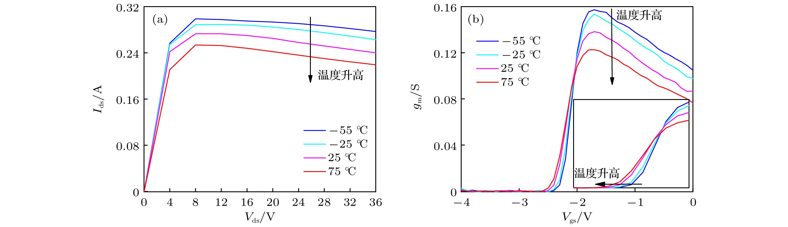
图 1 不同温度下GaN HEMT直流特性曲线 (a) 输出特性; (b)转移特性
Fig. 1. I-V characteristic curves of the GaN device under different ambient temperatures: (a) The transfer characteristics; (b) the output characteristics.
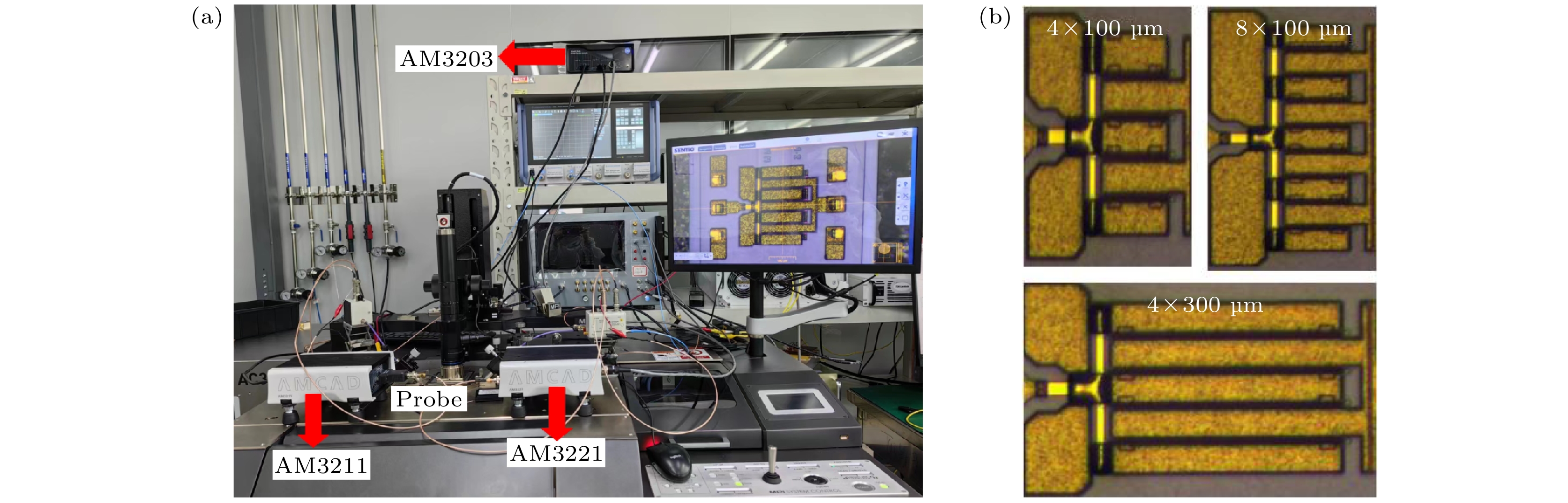
图 3 测试系统 (a) 直流特性测试平台; (b) 不同尺寸GaN HEMT实物图
Fig. 3. The test system: (a) Measurement for the DC characteristics; (b) photographs of GaN HEMTs.
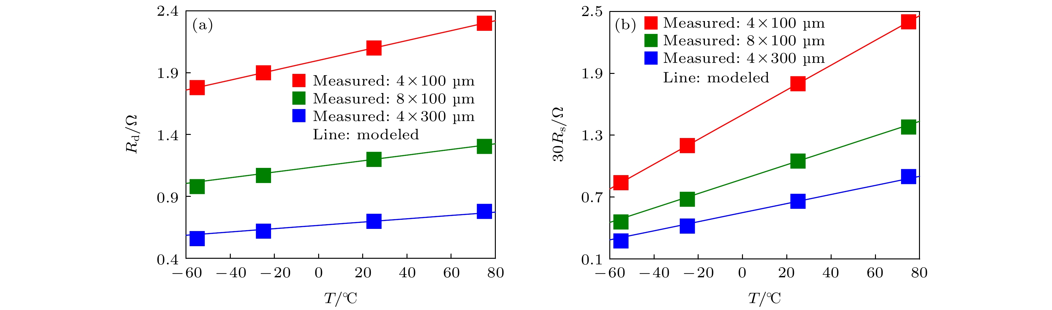
图 4 不同温度下仿真和实测的Rd/Rs对比
Fig. 4. Comparison between modeled and measured results of Rd and Rs under different temperatures.
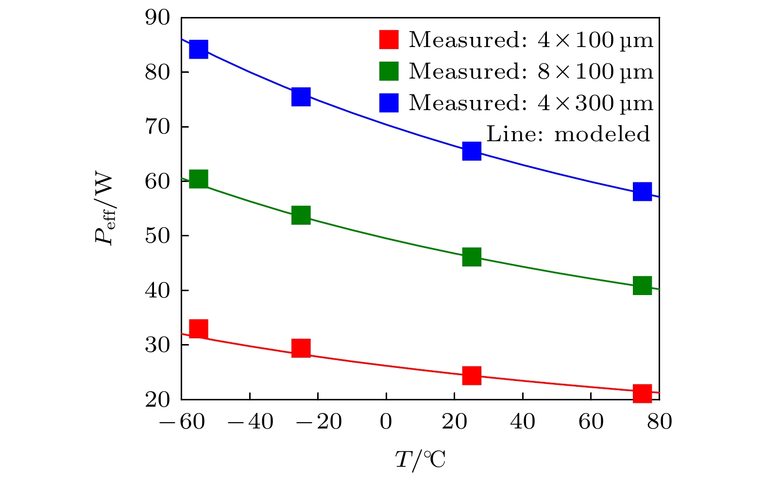
图 7 不同温度下仿真和实测的Peff对比
Fig. 7. Comparison between modeled and measured results of Peff under different temperatures.
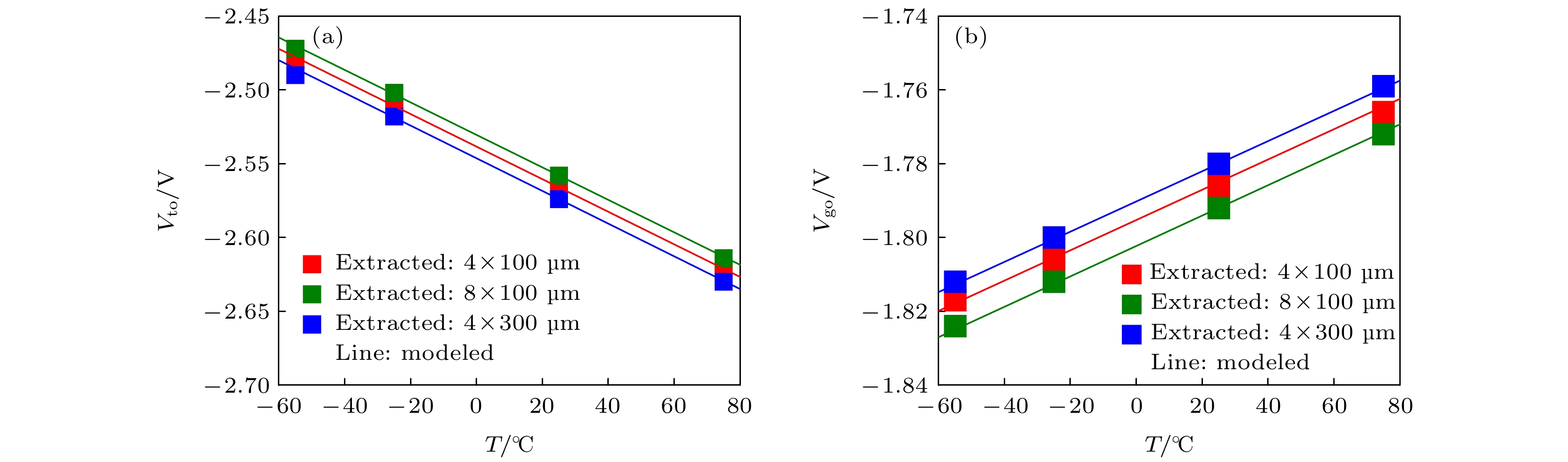
图 5 不同温度下仿真和实测的Vto和Vgo对比
Fig. 5. Comparison between modeled and measured results of Vto and Vgo under different temperatures.
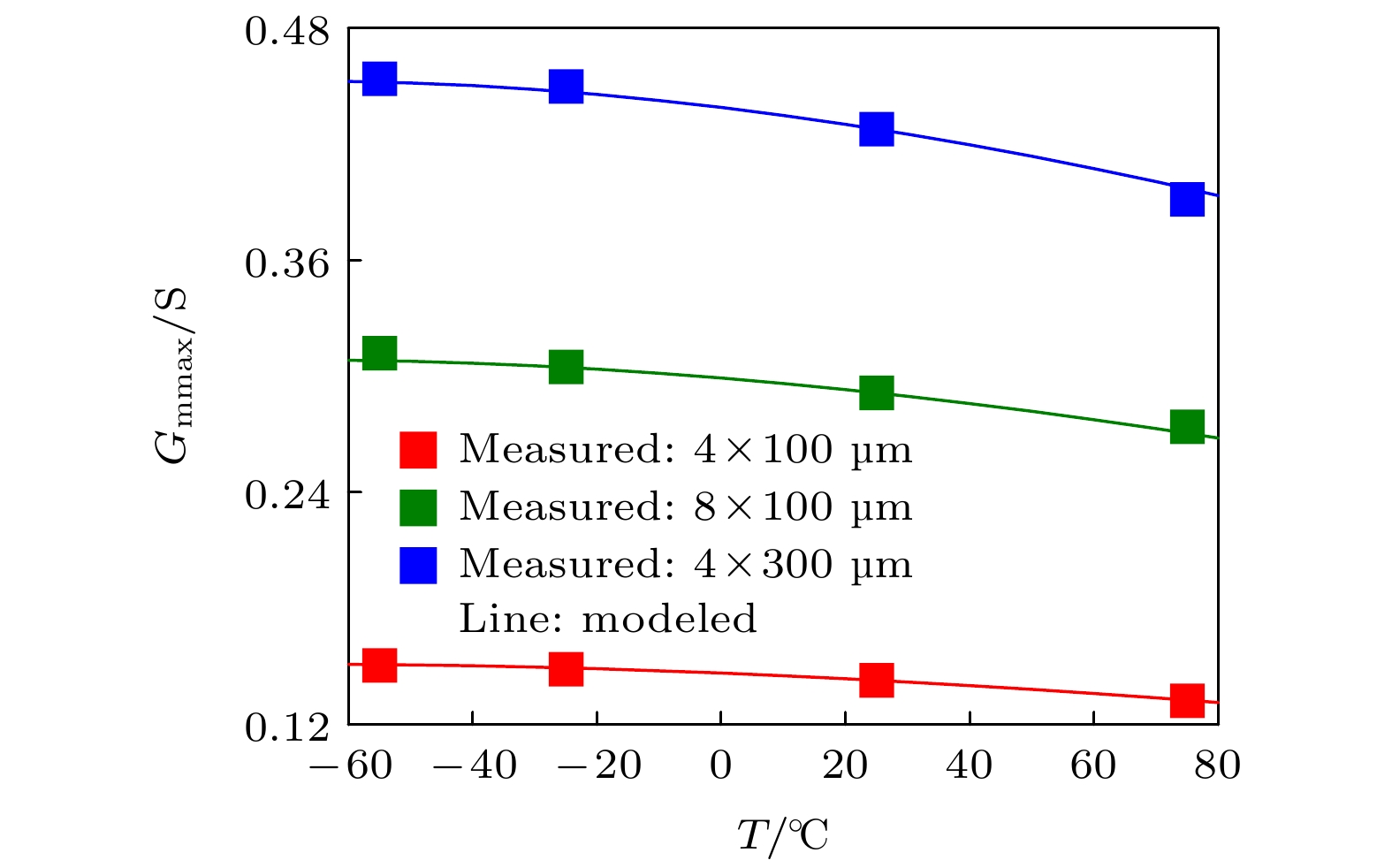
图 6 不同温度下仿真和实测的Gmmax对比
Fig. 6. Comparison between modeled and measured results of Gmmax under different temperatures.
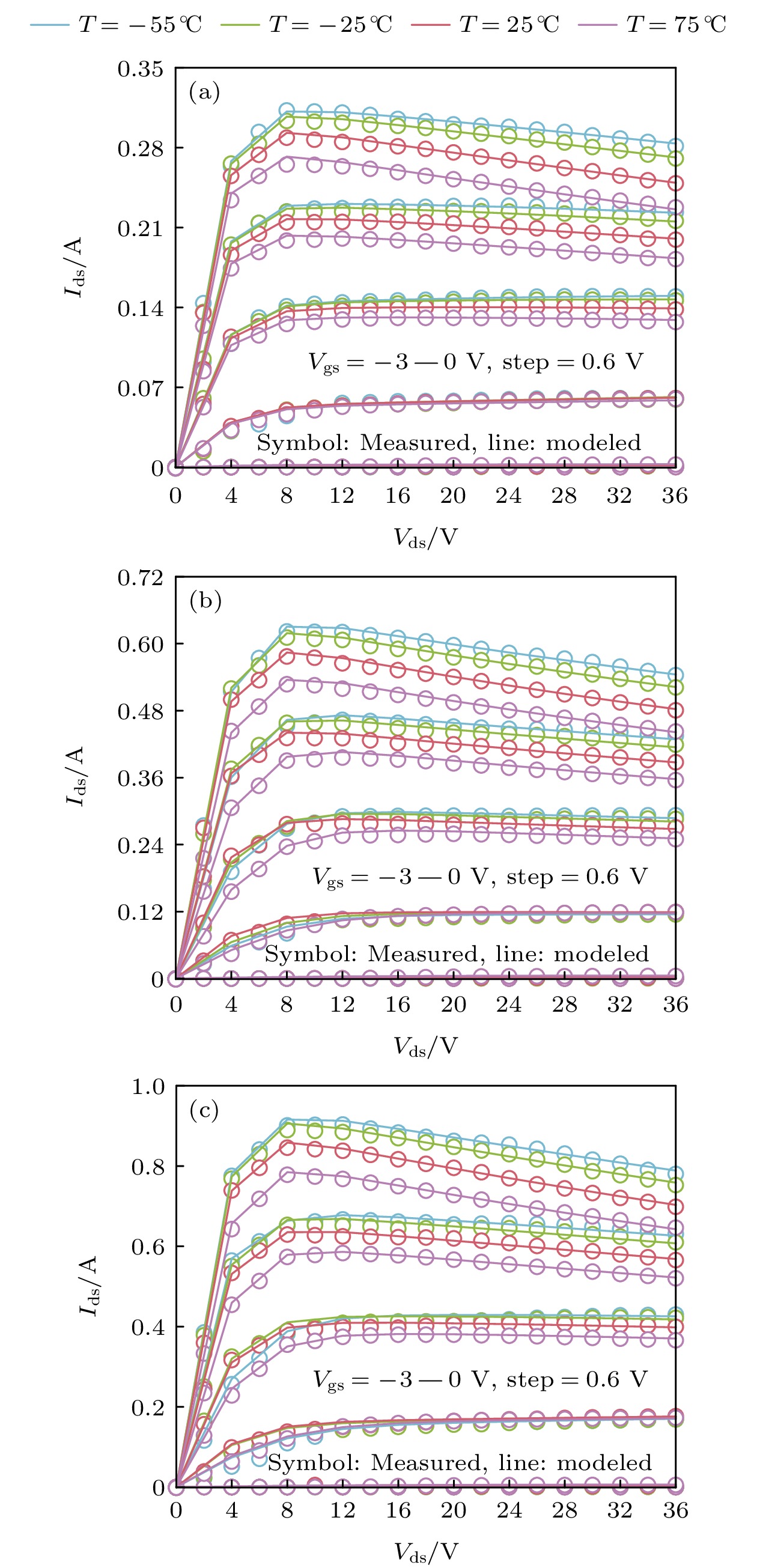
图 8 不同温度下输出特性拟合结果 (a) 400 μm器件; (b) 800 μm器件; (c) 1200 μm器件
Fig. 8. The fitting result of the output characteristics Ids-Vds under different ambient temperatures: (a) The 400-μm-wide device; (b) the 800-μm-wide device; (c) the 1200-μm-wide device.
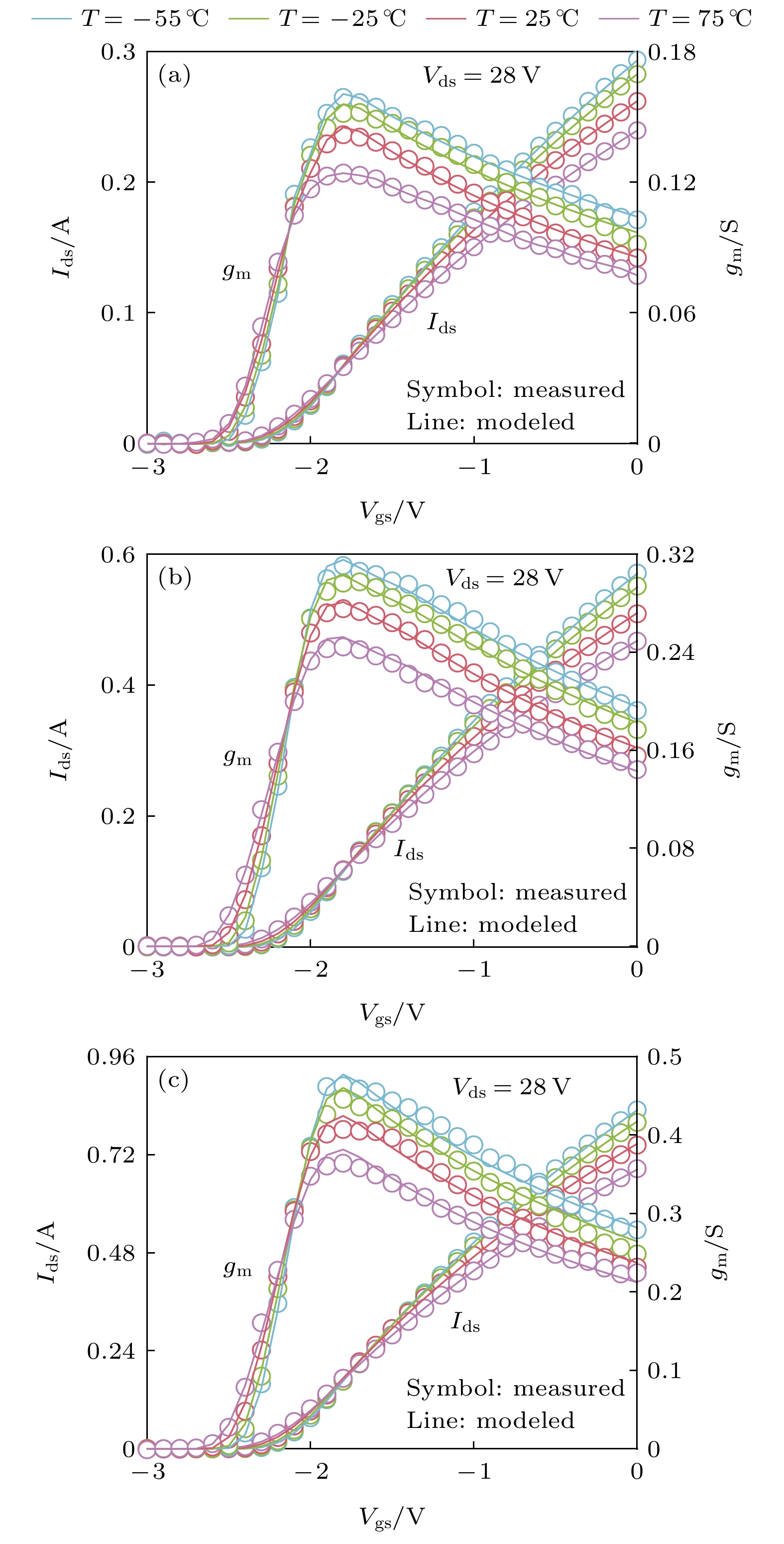
图 9 不同温度下转移特性拟合结果 (a) 400 μm器件; (b) 800 μm器件; (c) 1200 μm器件
Fig. 9. The fitting result of the transfer characteristics Ids-Vgs under different ambient temperatures: (a) The 400-μm-wide device; (b) the 800-μm-wide device; (c) the 1200-μm-wide device.
表 1 温度效应相关参数
Table 1. Values of the parameters related to temperature effect.
参数 Trd Trs Tvto Tvgo Tpeff Tgmmax1 Tgmmax2 数值 1.91×10⁻³ 6.67×10⁻³ 4.30×10⁻⁴ –2.30×10⁻⁴ –0.81 –2.66×10⁻³ 0.44  下载: 导出CSV
-
[1] Mishra U K, Parikh P, Wu Y F 2002 Proc. IEEE 90 1022
Google Scholar
[2] Quay R 2008 Gallium Nitride Electronics (Berlin: Springer-Verlag) pp23–30
[3] 赵正平 2015 半导体技术 40 1
Google Scholar
Zhao Z P 2015 Semicond. Tech. 40 1
Google Scholar
[4] Maas S A 2003 Nonlinear Microwave and RF Circuits Second Edition (Norwood: Artech House Publisher) pp29–55
[5] Baylis C, Dunleavy L, Connick R 2009 IEEE 10th Annual Wireless and Microwave Technology Conference Clearwater, USA, April 20–21, 2009 p1
[6] Eskanadri S, Hamedani F T 2012 Proceedings of the 19th International Conference Mixed Design of Integrated Circuits and Systems Warsaw, Poland, May 24–26, 2012 p360
[7] Hajji R, Poulton M, Crittenden D B, Gengler J, Xia P 2014 9th European Microwave Integrated Circuit Conference Rome, Italy, October 6–7, 2014 p373
[8] Darwish A M, Huebschman B D, Viveiros E, Hung H A 2009 IEEE T. Microw. Theory 57 3205
Google Scholar
[9] Ghosh S, Sharma K, Agnihotri S, Chauhan Y S, Khandelwal S, Fjeldly T A, Yigletu F M, Iñiguez B 2014 IEEE 2nd International Conference on Emerging Electronics Bengaluru, India, December 3–6, 2014 p1
[10] Huque M A, Eliza S A, Rahman T, Huq H F, Islam S K 2009 Solid-State Electron. 53 341
Google Scholar
[11] 林倩, 贾立宁, 胡单辉, 陈思维, 刘林盛, 刘畅, 刘建利 2022 南京邮电大学学报 42 42
Google Scholar
Lin Q, Jia L N, Hu D H, Chen S W, Liu L S, Liu C, Liu J L 2022 J. Nanjing Univ. Posts Telecommun. 42 42
Google Scholar
[12] Khan M K, Alim M A, Gaquiere C 2021 Microelectron. Eng. 238 111508
Google Scholar
[13] Tokuda H, Yamazaki J, Kuzuhara M 2010 J. Appl. Phys. 108 104509
Google Scholar
[14] Zomorrodian V, Pei Y, Mishra U K, York R A 2010 Phys. Status Solidi 7 2450
Google Scholar
[15] Chang Y H, Chang J J 2007 IEEE Conference on Electron Devices and Solid-State Circuits Tainan, Taiwan, December 20–22, 2007 p237
[16] Curtice W R 1980 IEEE T. Microw. Theory 28 448
Google Scholar
[17] Dhar J, Garg S K, Arora P K, Rana S S, 2007 International Symposium on Signals, Circuits and Systems Iasi, Romania, July 13–14, 2007 p1
[18] 成爱强, 王帅, 徐祖银, 贺瑾, 张天成, 包华广, 丁大志 2023 物理学报 72 147103
Google Scholar
Cheng A Q, Wang S, Zu Z Y, He J, Zhang T C, Bao H G, Ding D Z 2023 Acta Phys. Sin. 72 147103
Google Scholar
[19] 亚历克斯·利多, 约翰·斯其顿, 迈克尔·德·罗伊, 戴维·罗伊施 (段宝兴, 杨银堂译) 2018 氮化镓功率晶体—器件、电路与应用第二版 (北京: 机械工业出版社) 第36—37页
Alex L, John S, Michael D R, David R (translated by Duan B X, Yang Y T) 2008 GaN Transistors for Efficient Power Conversion Second Edition (Beijing: China Machine Press) pp36–37
[20] Cuerdo R, Pedrós J, Navarro A, Braña A F, Paul J L, Muñoz E, Calle F 2008 Mater. Electron. 19 189
Google Scholar
[21] Hatano M, Kunishio N, Chikaoka H, Yamazaki J, Makhzani Z B, Yafune N, Sakuno K, Hashimoto S, Akita K, Yamamoto Y, Kuzuhara M 2010 CS MANTECH Conference Oregon, USA, May 17–20, 2010 p101
[22] Zhang X B, Liu N Z, Yao R H 2020 Acta Phys. Sin. 69 157303 [张雪冰, 刘乃漳, 姚若河 2020 物理学报 69 157303]
Google Scholar
Zhang X B, Liu N Z, Yao R H 2020 Acta Phys. Sin. 69 157303
Google Scholar
[23] 任春江, 陈堂胜, 焦刚, 李肖 2007 固体电子学研究与进展 27 329
Google Scholar
Ren C J, Chen T S, Jiao G, Li X 2007 Res. Prog. Solid State Electron. 27 329
Google Scholar
[24] 高建军 2007 场效应晶体管射频微波建模技术 (北京: 电子工业出版) 第75—125页
Gao J J 2007 RF Microwave Modeling Technology for Field Effect Transistors (Beijing: Electronic Industry Publishing) pp75–125
[25] Wang Y H, Liang Y C, Samudra1 G S, Chang T F, Huang C F, Yuan L, Lo G Q 2013 Semicond. Sci. Tech. 28 125010
Google Scholar
[26] Islam S, Alim M A, Chowdhury A Z, Gaquiere C 2022 JTAC 147 10991
Google Scholar

 下载:
下载:
计量
- 文章访问数: 3993
- PDF下载量: 96
- 被引次数: 0
