


-
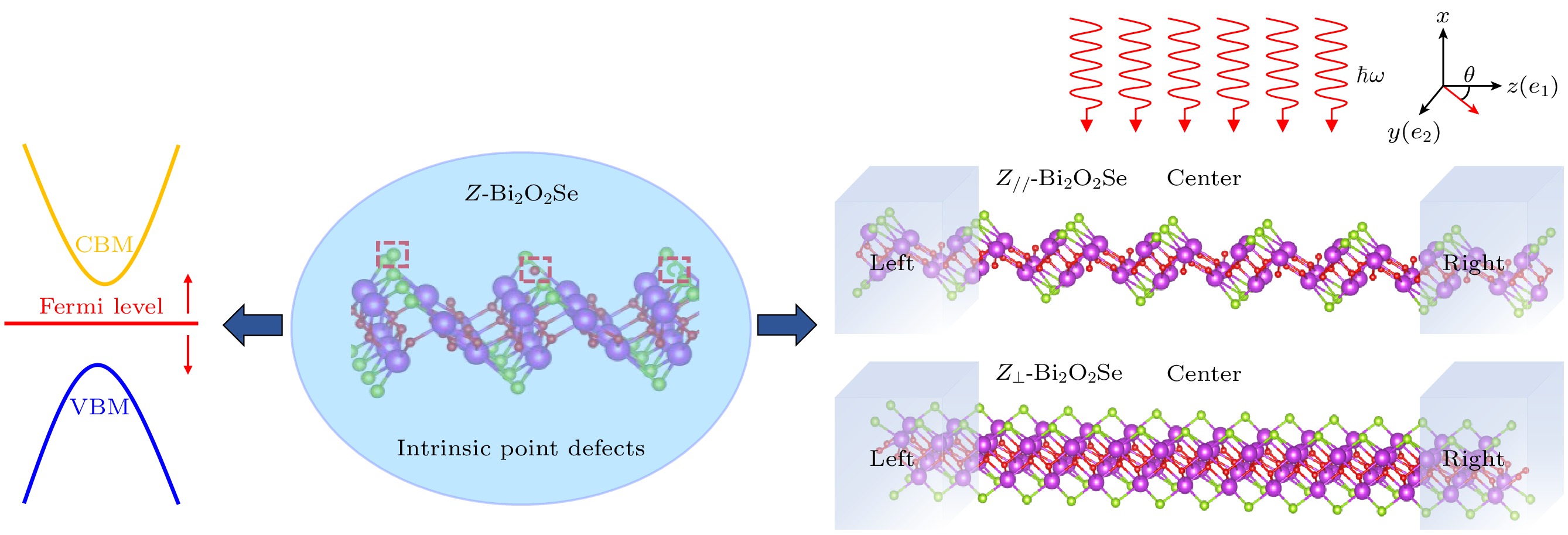
采用基于密度泛函理论的第一性原理和非平衡格林函数方法, 系统研究了单层拉链型硒氧化铋(Z-Bi2O2Se)中空位、反位和吸附点缺陷的结构、电子和光电性质. 通过在不同生长环境下形成能的计算发现, 点缺陷O' 空位, O取代Se反位、Se 吸附Bi'-Bi'-Se和Bi-Bi-Se穴位相对容易形成; 电子态密度及形成能的计算结果显示, O' 空位、Se吸附Bi'-Bi'-Se和Bi-Bi-Se穴位属于深能级n型掺杂. 此外, 沿平行和垂直拉链方向分别构建了基于单层Z-Bi2O2Se的器件, 其光电性能表现出明显的各向异性. 点缺陷的引入降低了体系对称性, 使其光电流在可见光区和紫外光区显著增大, 各向异性仍然存在. 点缺陷对器件消光比的影响同时取决于点缺陷类型及光子能量, 通过选择点缺陷在特定光子能量的照射可以有效提高器件的偏振灵敏度. 本文研究结果对深入认识二维Bi2O2Se结构及其性能提供理论指导.The novel layered semiconductor material bismuth oxyselenide (Bi2O2Se) exhibits exceptional properties such as thickness-dependent bandgap, superior electron mobility, compatibility with various materials, and stability under ambient conditions. The zipper-type two-dimensional Bi2O2Se (Z-Bi2O2Se) is a newly proposed structure based on theoretical studies of material surface dissociation mechanisms. However, current understanding of this structure still mainly focuses on fundamental investigations of electronic properties such as band structures. Intrinsic point defects, which are inevitable during material synthesis and operational environments, significantly influence the physical characteristics of materials and ultimately dictate device performance. In this work, we conduct an in-depth exploration of intrinsic point defects in the material. Using first-principles calculations based on density functional theory (DFT) and non-equilibrium Green’s function (NEGF) methods, we systematically investigate the structural, electronic, and optoelectronic properties of vacancies, antisites, and adatom point defects in Z-Bi2O2Se. First, the formation energy calculations under different growth conditions reveal that o'vacancy, Se replaced by O, Se adsorption on “Bi'-Bi'-Se” and “Bi-Bi-Se” hollow sites are relatively easy to form. The density of states (DOS) and formation energy shows that o'vacancy, Se adsorption on “Bi'-Bi'-Se” and “Bi-Bi-Se” hollow sites tend to lose electrons and become positively charged. Their donor levels are located at 0.78 eV, 0.01 eV, and 0.07 eV above the valence band maximum (VBM), but well below the conduction band minimum (CBM), indicating deep-level n-type doping characteristics. Furthermore, devices based on monolayer Z-Bi2O2Se along the parallel (Z//) direction and perpendicular (Z⊥) direction of the “zipper” structure are constructed to investigate the influence of intrinsic point defects on optoelectronic performance. The results show that for pristine materials, the photocurrent of Z⊥-perfect in the visible and ultraviolet regions is two orders of magnitude smaller than that of Z//-perfect, demonstrating significant anisotropy. The introduction of point defects reduces system’s symmetry, leading to a remarkable enhancement of photocurrent in both devices in these spectral regions. Notably, in the Z⊥ direction, the point defects induce the photocurrent to increase by three orders of magnitude. However, the photocurrent remains relatively small compared with that in Z// direction, indicating persistent anisotropy. The influence of point defects on the extinction ratio depends on both defect types and photon energy. By selecting specific point defects under irradiation at targeted photon energy, the polarization sensitivity of devices can be effectively improved. These findings provide theoretical guidance for deepening the understanding of the electronic structure and optoelectronic properties of two-dimensional Z-Bi2O2Se.
-
Keywords:
- first-principles calculation /
- non-equilibrium Green’s function /
- point defects /
- electronic and photoelectric properties
[1] Wu J X, Yuan H T, Meng M M, et al. 2017 Nature Nanotech. 12 530
 Google Scholar
[2] Fu H X, Wu J X, Peng H L, Yan B H 2018 Phys. Rev. B 95 241203
Google Scholar
[3] Wang C, Ding G Q, Wu X M, Wei S S, Gao G Y 2018 New J. Phys. 20 123014
Google Scholar
[4] Jiang H T, Xu X, Fan C, Dai B B, Qi Z D, Jiang S, Cai M Q, Zhang Q L 2022 Chin. Phys. B 31 048102
Google Scholar
[5] Li J, Wang Z X, Wen Y, Chu J, Yin L, Cheng R Q, Lei L, He P, Jiang C, Feng L P, He J 2018 Adv. Funct. Mater. 28 1706437
Google Scholar
[6] Tong T, Chen Y F, Qin S C, et al. 2019 Adv. Funct. Mater. 29 1905806
Google Scholar
[7] Liu B, Zhou H 2021 Chin. Phys. B 30 106803
Google Scholar
[8] Ding X, Li M L, Chen P, et al. 2022 Matter 5 4274
Google Scholar
[9] Tippireddy S, Prem Kumar D S, Das S, Mallik R C 2021 ACS Appl. Energy Mater. 4 2022
Google Scholar
[10] Wu J X, Tan C W, Tan Z J, Liu Y J, Yin J B, Dang W H, Wang M Z, Peng H L 2017 Nano. Lett. 17 3021
Google Scholar
[11] Liang Y, Chen Y J, Sun Y W, et al. 2019 Adv. Mater. 31 1901964
Google Scholar
[12] Wu J X, Qiu C G, Fu H X, et al. 2019 Nano. Lett. 19 197
Google Scholar
[13] Song Y K, Li Z J, Li H, et al. 2020 Nanotechnology 31 165704
Google Scholar
[14] Wang H, Zhang Z K, Luo H J, Zhang S Q, Pan W W, Liu J L, Ren Y L, Lei W 2024 Adv. Optical Mater. 12 2401404
Google Scholar
[15] Chen G X, Wu J, Wang B, Li J, Qi X 2020 Appl. Phys. A 126 579
Google Scholar
[16] Chen G X, Zhou Y, Zhang G B, Li J, Qi X 2021 Ceram. Int. 47 25255
Google Scholar
[17] 李丹阳, 韩旭, 徐光远, 刘筱, 赵枭钧, 李庚伟, 郝会颖, 董敬敬, 刘昊, 邢杰 2020 物理学报 69 248502
Google Scholar
Li D Y, Han X, Xu G Y, Liu X, Zhao X J, Li G W, Hao H Y, Dong J J, Liu H, Xing J 2020 Acta Phys. Sin. 69 248502
Google Scholar
[18] Khan U, Luo Y T, Tang L, Teng C J, Liu J M, Liu B L, Cheng H M 2019 Adv. Funct. Mater. 29 1807979
Google Scholar
[19] Wang N, Li M L, Xiao H Y, Gong H F, Liu Z J, Zu X T, Qiao L 2019 Phys. Chem. Chem. Phys. 21 15097
Google Scholar
[20] Tang H, Shi B W, Wang Y Y, Yang C, Liu S Q, Li Y, Quhe R G, Lu J 2021 Phys. Rev. Appl. 15 064037
Google Scholar
[21] Pang Z Q, Li T 2021 J. Mech. Phys. Solids 157 104626
Google Scholar
[22] Li J Q, Cheng C, Duan M Y 2023 Appl. Surf. Sci. 618 156541
Google Scholar
[23] Wei Q L, Li R P, Lin C Q, Han A, Nie A M, Li Y R, Li L J, Cheng Y C, Huang W 2019 ACS Nano. 13 13439
Google Scholar
[24] Ge Z C, Zhao W, Yuan S F, Gao Z X, Hao C L, Ma H, Ren H, Guo W Y 2023 Appl. Surf. Sci. 611 155528
Google Scholar
[25] Lu S C, Li Y L, Zhao X 2023 Phys. Chem. Chem. Phys. 25 19167
Google Scholar
[26] Hossain M T, Jena T, Debnath S, Giri P K 2023 J. Mater. Chem. C 11 6670
Google Scholar
[27] Li H L, Xu X T, Zhang Y, Gillen R, Shi L P, Robertson J 2018 Sci. Rep. 8 10920
Google Scholar
[28] Wei Q L, Lin C Q, Li Y F, Zhang X Y, Zhang Q Y, Shen Q, Cheng Y C, Huang W 2018 J. Appl. Phys. 124 055701
Google Scholar
[29] Wu Z, Wang Y, Liu G, Yang X, Wei T, Zhang H, Zhou J, Zhu J 2021 Mater. Today 21 100810
Google Scholar
[30] Kresse G, Furthmüller J 1996 Comput. Mater. Sci. 6 15
Google Scholar
[31] Kresse G, Hafner J 1993 Phys. Rev. B 47 558
Google Scholar
[32] Kresse G, Furthmüller J 1996 Phys. Rev. B 54 11169
Google Scholar
[33] Kresse G, Joubert D 1999 Phys. Rev. B 59 1758
Google Scholar
[34] Perdew J P, Burke K, Ernzerhof M 1996 Phys. Rev. Lett. 77 3865
Google Scholar
[35] Freysoldt C, Grabowski B, Hickel T, Neugebauer J, Kresse G, Janotti A, Van de Walle C G 2014 Rev. Mod. Phys. 86 253
Google Scholar
[36] Kohn W, Sham L J 1965 Phys. Rev. 140 A1133
Google Scholar
[37] Freysoldt C, Neugebauer J 2018 Phys. Rev. B 97 205425
Google Scholar
[38] Freysoldt C, Neugebauer J, Van de Walle C G 2009 Phys. Rev. Lett. 102 016402
Google Scholar
[39] Xue L, Sun L Z, Hao G L, Zhou P, He C Y, Huang Z Y, Zhong J X 2014 RSC Adv. 4 10499
Google Scholar
[40] Huang M L, Zheng Z N, Dai Z X, Guo X J, Wang S S, Jiang L L, Wei J C, Chen S Y 2022 J. Semicond. 43 042101
Google Scholar
[41] Fu Z T, Yan P L, Li J, Zhang S F, He C Y, Ouyang T, Zhang C X, Tang C, Zhong J X 2022 Nanoscale 14 11316
Google Scholar
[42] Taylor J, Guo H, Wang J 2001 Phys. Rev. B 63 245407
Google Scholar
[43] Zhang L, Gong K, Chen J Z, Liu L, Zhu Y, Xiao D, Guo H 2014 Phys. Rev. B 90 195428
Google Scholar
[44] Chen J Z, Hu Y B, Guo H 2012 Phys. Rev. B 85 155441
Google Scholar
[45] Chu F H, Chen M Y, Wang Y, Xie Y Q, Liu B Y, Yang Y H, An X T, Zhang Y Z 2018 J. Mater. Chem. C 6 2509
Google Scholar
[46] Xie Y Q, Zhang L, Zhu Y, Liu L, Guo H 2015 Nanotechnology 26 455202
Google Scholar
[47] Xu Z H, Luo B, Chen M Y, Xie W Z, Hu Y B, Xiao X B 2021 Appl. Surf. Sci. 548 148751
Google Scholar
[48] Belinicher V I 1978 Phys. Lett. A 66 213
Google Scholar
[49] Zhang L W, Yang Y Q, Chen J, Zhang L 2023 Front. Phys. 18 62301
Google Scholar
[50] Luo Y Z, Xie Y Q, Zhao J, Hu Y B, Ye X, Ke S H 2021 Phys. Rev. Mater. 5 054004
Google Scholar
[51] Zhao J, Hu Y B, Xie Y Q, Zhang L, Wang Y 2020 Phys. Rev. Appl. 14 064003
Google Scholar
[52] Sun X X, Yin S Q, Wei D, Li Y, Ma Y Q, Dai X Q 2023 Appl. Surf. Sci. 610 155401
Google Scholar
-
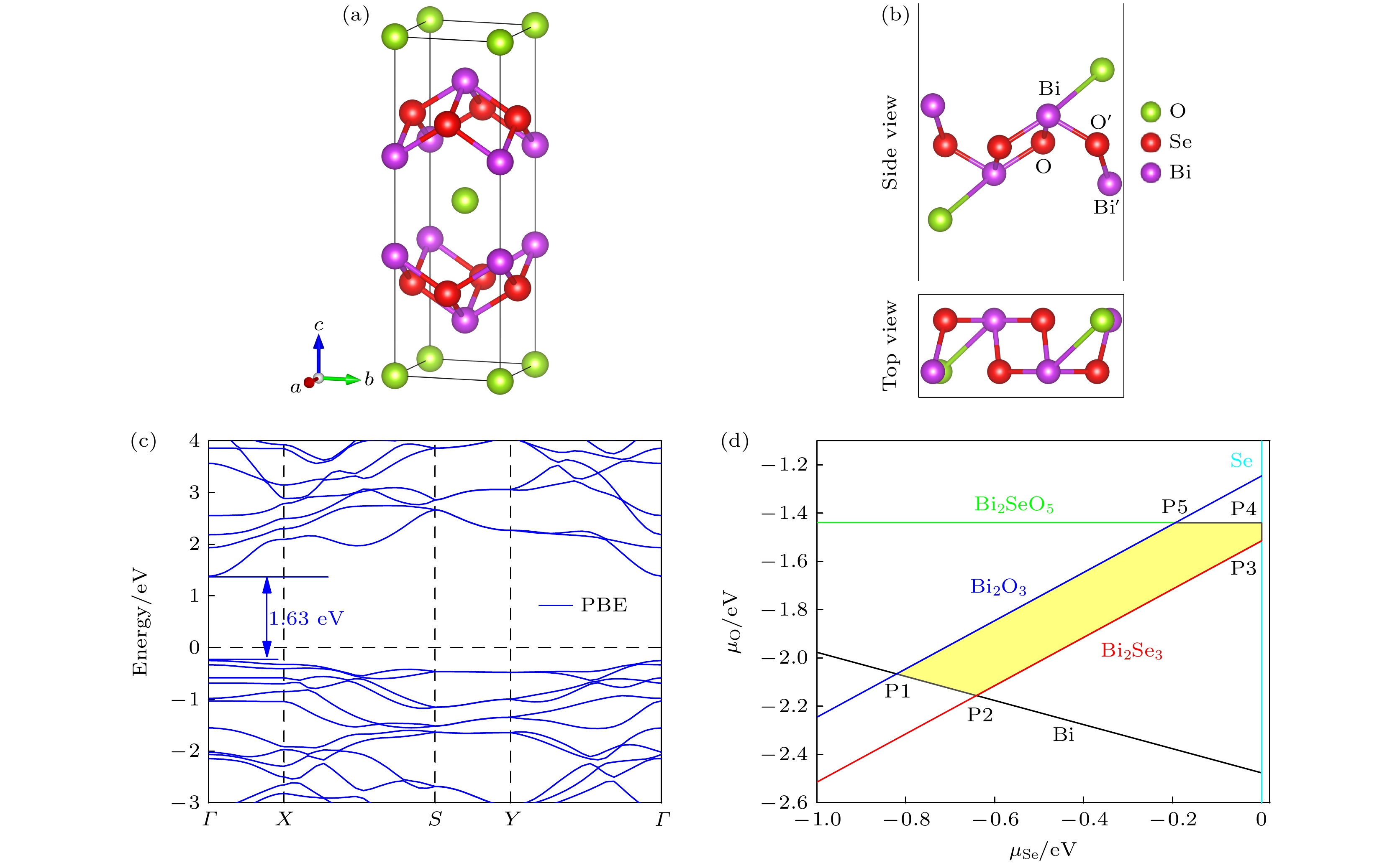
图 1 (a)块体 Bi2O2Se 的单胞结构; (b)单层 Z-Bi2O2Se 的侧视图及俯视图; (c)单层 Z-Bi2O2Se 的电子能带结构(蓝色为PBE方法); (d) Bi2O2Se 生长的化学势范围(黄色区域)
Fig. 1. (a) Unit cell structure of bulk Bi2O2Se; (b) the side and top views of monolayer Z-Bi2O2Se; (c) the electronic energy bands of the monolayer Z-Bi2O2Se (bule represents PBE); (d) the chemical potentials range for the growth of Bi2O2Se (the yellow part).
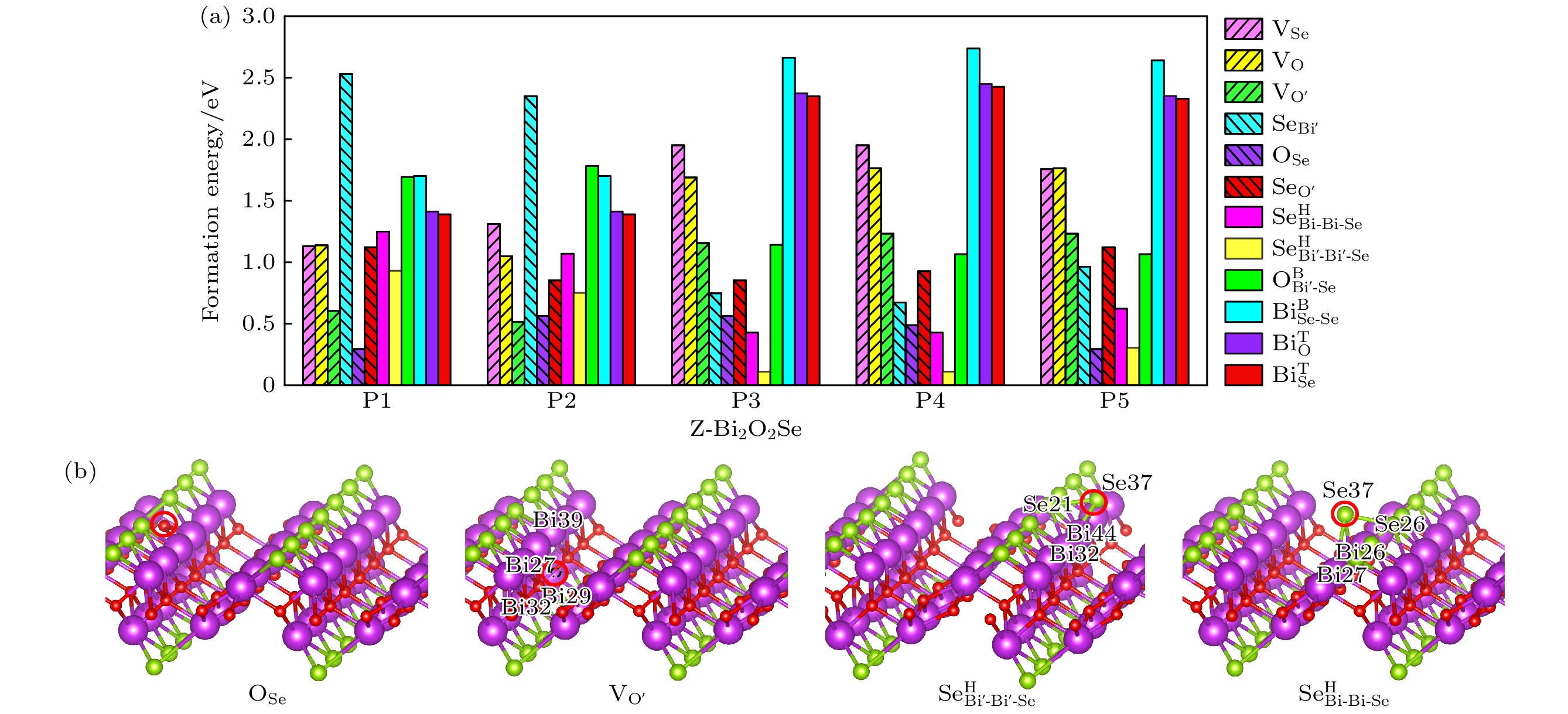
图 2 (a)在不同生长环境P1—P5时, 单层 Z-Bi2O2Se 中点缺陷的形成能; (b)单层 Z-Bi2O2Se 中点缺陷OSe, $\rm V_{O'}$, $ \text{Se}_{\text{Bi}'\text{-Bi}'\text{-Se}}^{\text{H}} $和$ {\text{Se}}_{{\text{Bi-Bi-Se}}}^{\text{H}} $的结构图
Fig. 2. (a) Formation energies of the point defects in monolayer Z-Bi2O2Se under different growth environments P1–P5; (b) the structures of the point defects OSe, $\rm V_{O'} $, $ \text{Se}_{\text{Bi}'\text{-Bi}'\text{-Se}}^{\text{H}} $ and $ {\text{Se}}_{{\text{Bi-Bi-Se}}}^{\text{H}} $ in monolayer Z-Bi2O2Se.
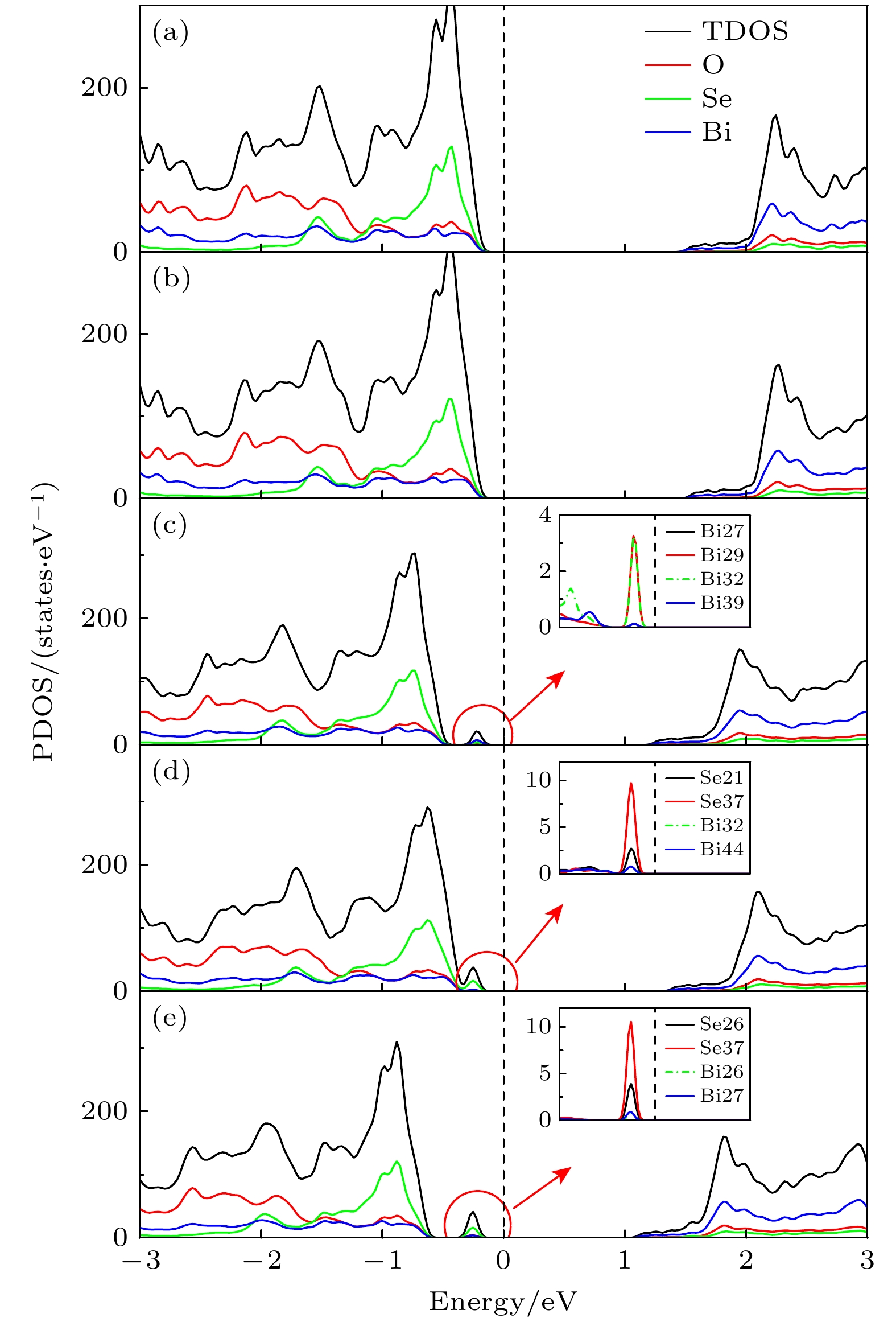
图 3 (a) Z-Bi2O2Se 完整体系与含 (b) OSe, (c) $\rm V_{O'} $, (d) $ \text{Se}_{\text{Bi}'\text{-Bi}'\text{-Se}}^{\text{H}} $, (e) $ {\text{Se}}_{{\text{Bi-Bi-Se}}}^{\text{H}} $ 点缺陷体系总态密度和投影态密度图, 插图为杂质态部分原子投影态密度
Fig. 3. The TDOS and PDOS of (a) the perfect Z-Bi2O2Se and (b) OSe, (c) $\rm V_{O'} $, (d) $ \text{Se}_{\text{Bi}'\text{-Bi}'\text{-Se}}^{\text{H}}$, (e) $ {\text{Se}}_{{\text{Bi-Bi-Se}}}^{\text{H}} $ doped systems, and the insets are the enlarge views of the impurity states.
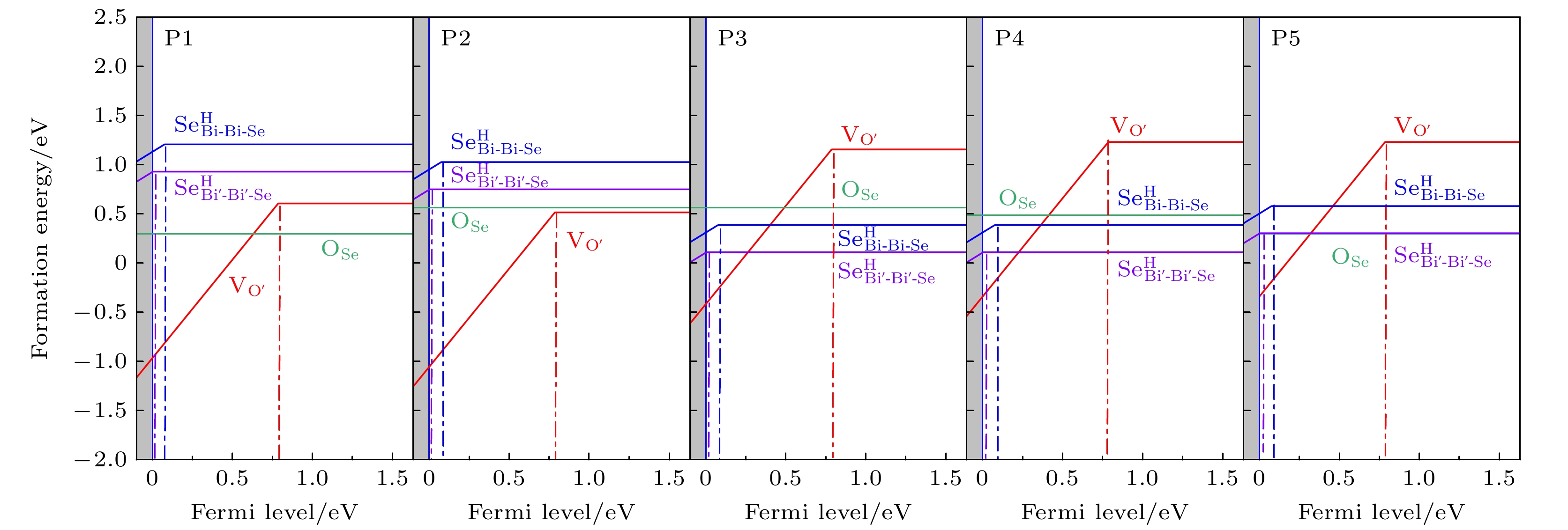
图 4 不同化学势条件(P1, P2, P3, P4, P5)下, 点缺陷OSe, $\rm V_{O'} $, $ \text{Se}_{\text{Bi}'\text{-Bi}'\text{-Se}}^{\text{H}} $和$ {\text{Se}}_{{\text{Bi-Bi-Se}}}^{\text{H}} $的形成能随费米能级的变化(将VBM处设置为零点, 线的斜率表示缺陷在该费米能级处的电荷态)
Fig. 4. Formation energies of point defects (OSe, $\rm V_{O'} $, $ \text{Se}_{\text{Bi}'\text{-Bi}'\text{-Se}}^{\text{H}} $and $ {\text{Se}}_{{\text{Bi-Bi-Se}}}^{\text{H}} $) in Bi2O2Se are as a function of the Fermi level under different chemical potential conditions (P1–P5). For all cases, the VBM are set for zero. The slope of the lines gives the charge state at the Fermi level.
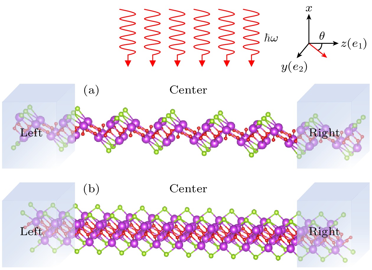
图 5 线偏振光照射下(a)单层 Z//-Bi2O2Se和(b)单层 Z⊥-Bi2O2Se 光电探测器结构示意图
Fig. 5. Schematic structures of (a) monolayer Z//-Bi2O2Se and (b) monolayer Z⊥-Bi2O2Se photodetectors under the linearly polarized light.
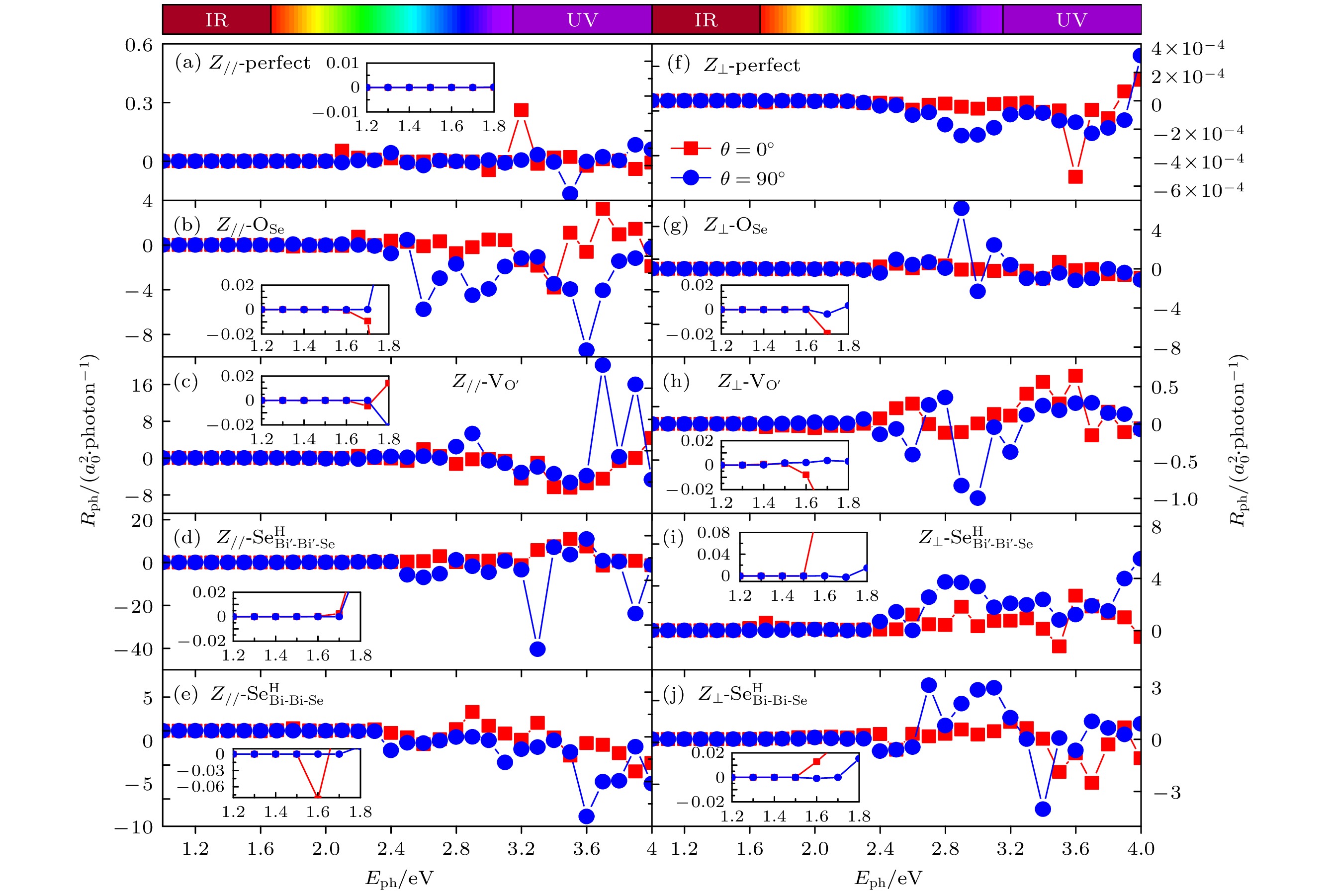
图 6 基于单层 Z//-Bi2O2Se和 Z⊥-Bi2O2Se 完整结构和含点缺陷OSe, $\rm V_{O'} $, $ \text{Se}_{\text{Bi}'\text{-Bi}'\text{-Se}}^{\text{H}} $和$ {\text{Se}}_{{\text{Bi-Bi-Se}}}^{\text{H}} $的器件在θ = 0° 和 θ = 90° 线偏振光照射下的光电流(插图为低光子能量区域放大图)
Fig. 6. Photocurrents functions of the devices based on perfect and OSe, $\rm V_{O'} $, $ \text{Se}_{\text{Bi}'\text{-Bi}'\text{-Se}}^{\text{H}} $, $ {\text{Se}}_{{\text{Bi-Bi-Se}}}^{\text{H}} $doped monolayer Z//-Bi2O2Se and Z⊥-Bi2O2Se under θ = 0° and θ = 90° linearly polarized light (the insets are the enlarged views of the low-photo-energy region).
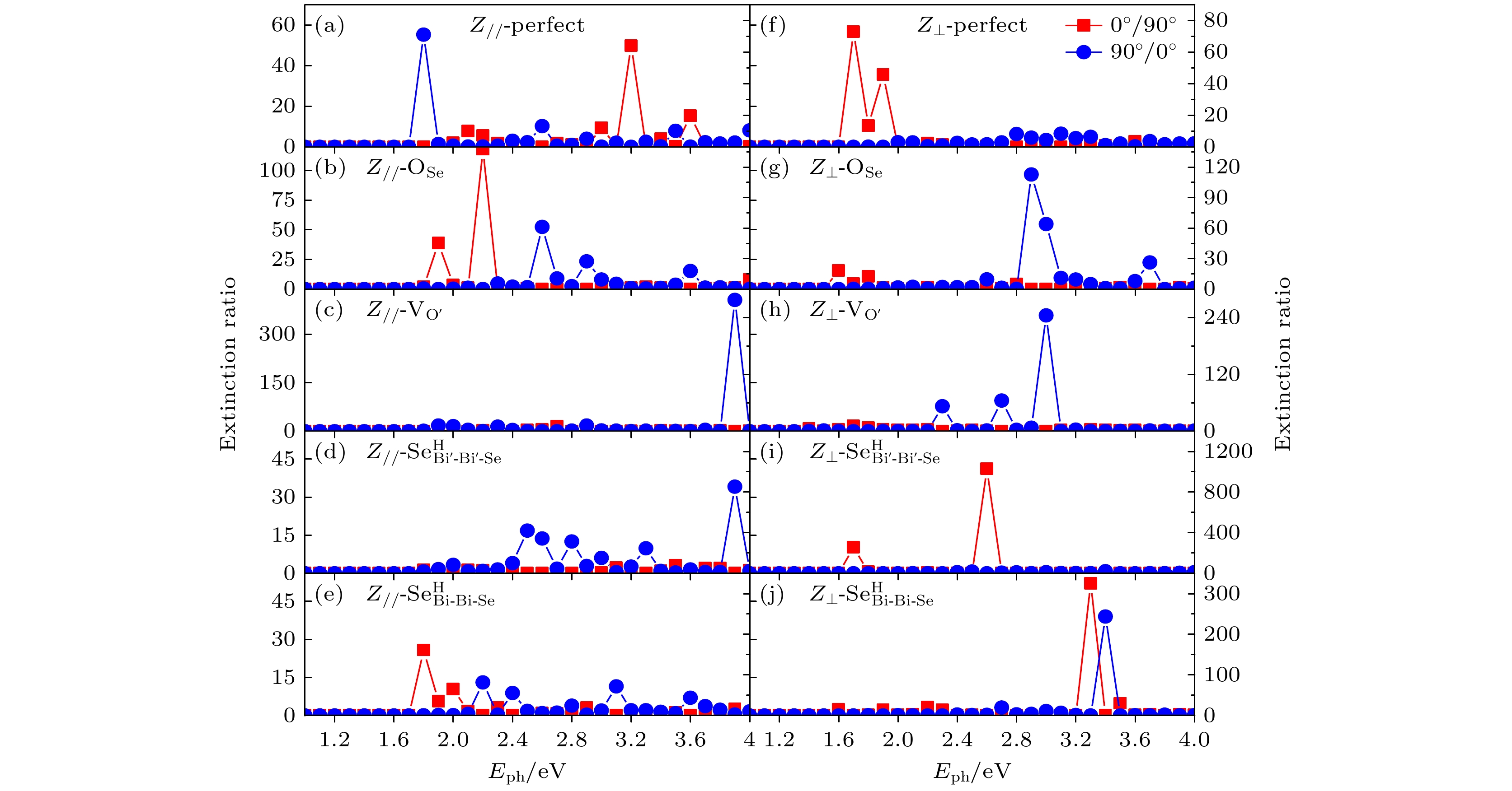
图 7 单层 Z//-Bi2O2Se和 Z⊥-Bi2O2Se 完整结构和含点缺陷OSe, $\rm V_{O'} $, $ \text{Se}_{\text{Bi}'\text{-Bi}'\text{-Se}}^{\text{H}} $和$ {\text{Se}}_{{\text{Bi-Bi-Se}}}^{\text{H}} $器件在不同光子能量下的消光比
Fig. 7. Extinction ratios of devices based on perfect and OSe, $\rm V_{O'} $, $ \text{Se}_{\text{Bi}'\text{-Bi}'\text{-Se}}^{\text{H}} $ and $ {\text{Se}}_{{\text{Bi-Bi-Se}}}^{\text{H}} $ doped monolayer Z//-Bi2O2Se and Z⊥-Bi2O2Se at different photon energies.
表 1 图1(d)中5个临界点 P1—P5 对应的O, Se, Bi的化学势$ {\mu _\text{O}} $, $ {\mu _\text{Se}} $, $ {\mu _{{\text{Bi}}}} $(单位: eV)
Table 1. Chemical potentials of O, Se and Bi ($ {\mu _\text{O}} $, $ {\mu _\text{Se}} $, $ {\mu _{{\text{Bi}}}} $) corresponding to the five critical points P1–P5 in Fig. 1(d) (unit: eV).
P1 P2 P3 P4 P5 $ {\mu _\text{O}} $ –2.07 –2.16 –1.51 –1.44 –1.44 $ {\mu _\text{Se}} $ –0.82 –0.64 0.00 0.00 –0.19 $ {\mu _{{\text{Bi}}}} $ 0.00 0.00 –0.96 –1.04 –0.94  下载: 导出CSV
-
[1] Wu J X, Yuan H T, Meng M M, et al. 2017 Nature Nanotech. 12 530
Google Scholar
[2] Fu H X, Wu J X, Peng H L, Yan B H 2018 Phys. Rev. B 95 241203
Google Scholar
[3] Wang C, Ding G Q, Wu X M, Wei S S, Gao G Y 2018 New J. Phys. 20 123014
Google Scholar
[4] Jiang H T, Xu X, Fan C, Dai B B, Qi Z D, Jiang S, Cai M Q, Zhang Q L 2022 Chin. Phys. B 31 048102
Google Scholar
[5] Li J, Wang Z X, Wen Y, Chu J, Yin L, Cheng R Q, Lei L, He P, Jiang C, Feng L P, He J 2018 Adv. Funct. Mater. 28 1706437
Google Scholar
[6] Tong T, Chen Y F, Qin S C, et al. 2019 Adv. Funct. Mater. 29 1905806
Google Scholar
[7] Liu B, Zhou H 2021 Chin. Phys. B 30 106803
Google Scholar
[8] Ding X, Li M L, Chen P, et al. 2022 Matter 5 4274
Google Scholar
[9] Tippireddy S, Prem Kumar D S, Das S, Mallik R C 2021 ACS Appl. Energy Mater. 4 2022
Google Scholar
[10] Wu J X, Tan C W, Tan Z J, Liu Y J, Yin J B, Dang W H, Wang M Z, Peng H L 2017 Nano. Lett. 17 3021
Google Scholar
[11] Liang Y, Chen Y J, Sun Y W, et al. 2019 Adv. Mater. 31 1901964
Google Scholar
[12] Wu J X, Qiu C G, Fu H X, et al. 2019 Nano. Lett. 19 197
Google Scholar
[13] Song Y K, Li Z J, Li H, et al. 2020 Nanotechnology 31 165704
Google Scholar
[14] Wang H, Zhang Z K, Luo H J, Zhang S Q, Pan W W, Liu J L, Ren Y L, Lei W 2024 Adv. Optical Mater. 12 2401404
Google Scholar
[15] Chen G X, Wu J, Wang B, Li J, Qi X 2020 Appl. Phys. A 126 579
Google Scholar
[16] Chen G X, Zhou Y, Zhang G B, Li J, Qi X 2021 Ceram. Int. 47 25255
Google Scholar
[17] 李丹阳, 韩旭, 徐光远, 刘筱, 赵枭钧, 李庚伟, 郝会颖, 董敬敬, 刘昊, 邢杰 2020 物理学报 69 248502
Google Scholar
Li D Y, Han X, Xu G Y, Liu X, Zhao X J, Li G W, Hao H Y, Dong J J, Liu H, Xing J 2020 Acta Phys. Sin. 69 248502
Google Scholar
[18] Khan U, Luo Y T, Tang L, Teng C J, Liu J M, Liu B L, Cheng H M 2019 Adv. Funct. Mater. 29 1807979
Google Scholar
[19] Wang N, Li M L, Xiao H Y, Gong H F, Liu Z J, Zu X T, Qiao L 2019 Phys. Chem. Chem. Phys. 21 15097
Google Scholar
[20] Tang H, Shi B W, Wang Y Y, Yang C, Liu S Q, Li Y, Quhe R G, Lu J 2021 Phys. Rev. Appl. 15 064037
Google Scholar
[21] Pang Z Q, Li T 2021 J. Mech. Phys. Solids 157 104626
Google Scholar
[22] Li J Q, Cheng C, Duan M Y 2023 Appl. Surf. Sci. 618 156541
Google Scholar
[23] Wei Q L, Li R P, Lin C Q, Han A, Nie A M, Li Y R, Li L J, Cheng Y C, Huang W 2019 ACS Nano. 13 13439
Google Scholar
[24] Ge Z C, Zhao W, Yuan S F, Gao Z X, Hao C L, Ma H, Ren H, Guo W Y 2023 Appl. Surf. Sci. 611 155528
Google Scholar
[25] Lu S C, Li Y L, Zhao X 2023 Phys. Chem. Chem. Phys. 25 19167
Google Scholar
[26] Hossain M T, Jena T, Debnath S, Giri P K 2023 J. Mater. Chem. C 11 6670
Google Scholar
[27] Li H L, Xu X T, Zhang Y, Gillen R, Shi L P, Robertson J 2018 Sci. Rep. 8 10920
Google Scholar
[28] Wei Q L, Lin C Q, Li Y F, Zhang X Y, Zhang Q Y, Shen Q, Cheng Y C, Huang W 2018 J. Appl. Phys. 124 055701
Google Scholar
[29] Wu Z, Wang Y, Liu G, Yang X, Wei T, Zhang H, Zhou J, Zhu J 2021 Mater. Today 21 100810
Google Scholar
[30] Kresse G, Furthmüller J 1996 Comput. Mater. Sci. 6 15
Google Scholar
[31] Kresse G, Hafner J 1993 Phys. Rev. B 47 558
Google Scholar
[32] Kresse G, Furthmüller J 1996 Phys. Rev. B 54 11169
Google Scholar
[33] Kresse G, Joubert D 1999 Phys. Rev. B 59 1758
Google Scholar
[34] Perdew J P, Burke K, Ernzerhof M 1996 Phys. Rev. Lett. 77 3865
Google Scholar
[35] Freysoldt C, Grabowski B, Hickel T, Neugebauer J, Kresse G, Janotti A, Van de Walle C G 2014 Rev. Mod. Phys. 86 253
Google Scholar
[36] Kohn W, Sham L J 1965 Phys. Rev. 140 A1133
Google Scholar
[37] Freysoldt C, Neugebauer J 2018 Phys. Rev. B 97 205425
Google Scholar
[38] Freysoldt C, Neugebauer J, Van de Walle C G 2009 Phys. Rev. Lett. 102 016402
Google Scholar
[39] Xue L, Sun L Z, Hao G L, Zhou P, He C Y, Huang Z Y, Zhong J X 2014 RSC Adv. 4 10499
Google Scholar
[40] Huang M L, Zheng Z N, Dai Z X, Guo X J, Wang S S, Jiang L L, Wei J C, Chen S Y 2022 J. Semicond. 43 042101
Google Scholar
[41] Fu Z T, Yan P L, Li J, Zhang S F, He C Y, Ouyang T, Zhang C X, Tang C, Zhong J X 2022 Nanoscale 14 11316
Google Scholar
[42] Taylor J, Guo H, Wang J 2001 Phys. Rev. B 63 245407
Google Scholar
[43] Zhang L, Gong K, Chen J Z, Liu L, Zhu Y, Xiao D, Guo H 2014 Phys. Rev. B 90 195428
Google Scholar
[44] Chen J Z, Hu Y B, Guo H 2012 Phys. Rev. B 85 155441
Google Scholar
[45] Chu F H, Chen M Y, Wang Y, Xie Y Q, Liu B Y, Yang Y H, An X T, Zhang Y Z 2018 J. Mater. Chem. C 6 2509
Google Scholar
[46] Xie Y Q, Zhang L, Zhu Y, Liu L, Guo H 2015 Nanotechnology 26 455202
Google Scholar
[47] Xu Z H, Luo B, Chen M Y, Xie W Z, Hu Y B, Xiao X B 2021 Appl. Surf. Sci. 548 148751
Google Scholar
[48] Belinicher V I 1978 Phys. Lett. A 66 213
Google Scholar
[49] Zhang L W, Yang Y Q, Chen J, Zhang L 2023 Front. Phys. 18 62301
Google Scholar
[50] Luo Y Z, Xie Y Q, Zhao J, Hu Y B, Ye X, Ke S H 2021 Phys. Rev. Mater. 5 054004
Google Scholar
[51] Zhao J, Hu Y B, Xie Y Q, Zhang L, Wang Y 2020 Phys. Rev. Appl. 14 064003
Google Scholar
[52] Sun X X, Yin S Q, Wei D, Li Y, Ma Y Q, Dai X Q 2023 Appl. Surf. Sci. 610 155401
Google Scholar

 下载:
下载:
计量
- 文章访问数: 2141
- PDF下载量: 46
- 被引次数: 0
