


-
In this paper, the Tamm plasmon and its interaction with excitons in a plasmon microcavity consisting of metasurface, dielectric spacer, distributed Bragg reflector (DBR) are studied. The reflection phase of light on the surface can be controlled by changing the structure parameters in the metasurface. When the thickness of the dielectric spacer layer of the microcavity structure keeps unchanged, the resonance position of the Tamm plasmon mode supported by the microcavity structure can be adjusted by varying the structure parameters of the metasurface, and thus providing more degrees of freedom for regulating the Tamm plasmon mode. In addition, by comparing the traditional metal thin film-dielectric spacer-DBR structure, we find that the introduction of metasurface and its regulation of reflection phase can make the metasurface-dielectric spacer-DBR structure support the Tamm plasmon mode resonance at the same wavelength under a smaller thickness of spacer. And combining the local characteristics of the super-surface field, the model volume of Tamm plasmon can be reduced effectively. On this basis, we compare the interaction of traditional and metasurface-based Tamm plasmon with single-layer tungsten disulfide (WS2), and find that metasurface-based Tamm plasmon can produce stronger photon-exciton coupling and obtain larger Rabi splitting.
-
Keywords:
- surface plasmon /
- metasurface /
- two-dimensional materials /
- strong Coupling
[1] Gramotnev D K, Bozhevolnyi S I 2010 Nat. Photonics 4 83
 Google Scholar
[2] Schuller J A, Barnard E S, Cai W, Jun Y C, White J S, Brongersma M L 2010 Nat. Mater. 9 193
Google Scholar
[3] McFarland A D, Van Duyne R P 2013 Nano Lett. 3 1057
[4] Kinkhabwala A, Yu Z, Fan S, Avlasevich Y, Müllen K, Moerner W E 2009 Nat. Photonics 3 654
Google Scholar
[5] Schietinger S, Barth M, Aichele T, Benson O 2009 Nano Lett. 9 1694
Google Scholar
[6] Xu H, Bjerneld E J, Käll M, Börjesson L 1999 Phys. Rev. Lett. 83 4357
Google Scholar
[7] Vasa P, Wang W, Pomraenke R, Lammers M, Maiuri M, Manzoni C, Cerullo G, Lienau C 2013 Nat. Photonics 7 128
Google Scholar
[8] Santhosh K, Bitton O, Chuntonov L, Haran G 2016 Nat. Commun. 7 11823
Google Scholar
[9] Shi L, Hakala T K, Rekola H T, Martikainen J P, Moerland R J, Törmä P 2014 Phys. Rev. Lett. 112 153002
Google Scholar
[10] Ramezani M, Le-Van Q, Halpin A, Rivas J G 2018 Phys. Rev. Lett. 121 243904
Google Scholar
[11] Bellessa J, Symonds C, Vynck K, Lemaitre A, Brioude A, Beaur L, Plenet J C, Viste P, Fellbacq D, Cambrll E, Valvin P 2009 Phys. Rev. B 80 033303
Google Scholar
[12] 赵泽宇, 刘晋侨, 李爱, 武徐颖 2016 物理学报 65 231101
Google Scholar
Zhao Z Y, Liu J Q, Li A W, Xu X Y 2016 Acta Phys. Sin. 65 231101
Google Scholar
[13] Coles D M, Yang Y, Wang Y, Grant R T, Taylor R A, Saikin S K, Aspuru-Guzik A, Lidzey D G, Tang J K, Smith J M 2014 Nat. Commun. 5 5561
Google Scholar
[14] Todorov Y, Andrews A M, Sagnes I, Colombelli R, Klang P, Strasser G, Sirtori C 2009 Phys. Rev. Lett. 102 186402
Google Scholar
[15] Schwartz T, Hutchison J A, Genet C, Ebbesen T W 2011 Phys. Rev. Lett. 106 196405
Google Scholar
[16] Wurdack M, Lundt N, Klaas M, Baumann V, Kavokin A V, Höfling S, Schneider C 2017 Nat. Commun. 8 259
Google Scholar
[17] Lundt N, Klembt S, Cherotchenko E, Betzold S, Iff O, Nalitov A V, Klaas M, Dietrich C P, Kavokin A V, Höfling S, Schneider C 2016 Nat. Commun. 7 13328
Google Scholar
[18] Yu N, Aieta F, Genevet P, Kats M A, Gaburro Z, Capasso F 2012 Nano Lett. 12 6328
Google Scholar
[19] Yu N, Genevet P, Kats M A, Aieta F, Tetienne J P, Capasso F, Gaburro Z 2011 Science 334 333
Google Scholar
[20] Yang Y, Wang W, Moitra P, Kravchenko I I, Briggs D P, Valentine J 2014 Nano Lett. 14 1394
Google Scholar
[21] Jiang S C, Xiong X, Hu Y S, Hu Y H, Ma G B, Peng R W, Sun C, Wang M 2014 Phys. Rev. X 4 021026
[22] Lin D, Fan P, Hasman E, Brongersma M L 2014 Science 345 298
Google Scholar
[23] Zheng G, Mühlenbernd H, Kenney M, Li G, Zentgraf T, Zhang S 2015 Nat. Nanotechnol. 10 308
Google Scholar
[24] Wang S, Wu P C, Su V C, Lai Y C, Chen M K, Kuo H Y, Chen B H, Huang T T, Wang J H, Lin R M, Kuan C H, Li T, Wang Z, Tsai D P 2018 Nat. Nanotechnol. 13 227
Google Scholar
[25] Deng Z L, Deng J, Zhuang X, Wang S, Li K, Wang Y, Chi Y, Ye X, Xu J, Wang G P, Zhao R, Wang X, Cao Y, Cheng X, Li G, Li X 2018 Nano Lett. 18 2885
Google Scholar
[26] Wang S, Li F, Deng J, Ye X, Deng Z L, Cao Y, Guan B O, Li G, Li X 2019 J. Phys. D: Appl. Phys. 52 324002
Google Scholar
[27] Blaber M G, Arnold M D, Ford M J 2009 J. Phys. Chem. C 113 3041
[28] Dai Y, Ren W, Cai H, Ding H, Pan N, Wang X 2014 Opt. Express 22 7465
Google Scholar
[29] Liu W, Lee B, Naylor C H, Ee H S, Park J, Johnson A C, Agarwal R 2016 Nano Lett. 16 1262
Google Scholar
[30] Li Y, Chernikov A, Zhang X, Rigosi A, Hill H M, van der Zande A M, Chenet D A, Shih E M, Hone J, Heinz T F 2014 Phys. Rev. B 90 205422
Google Scholar
-
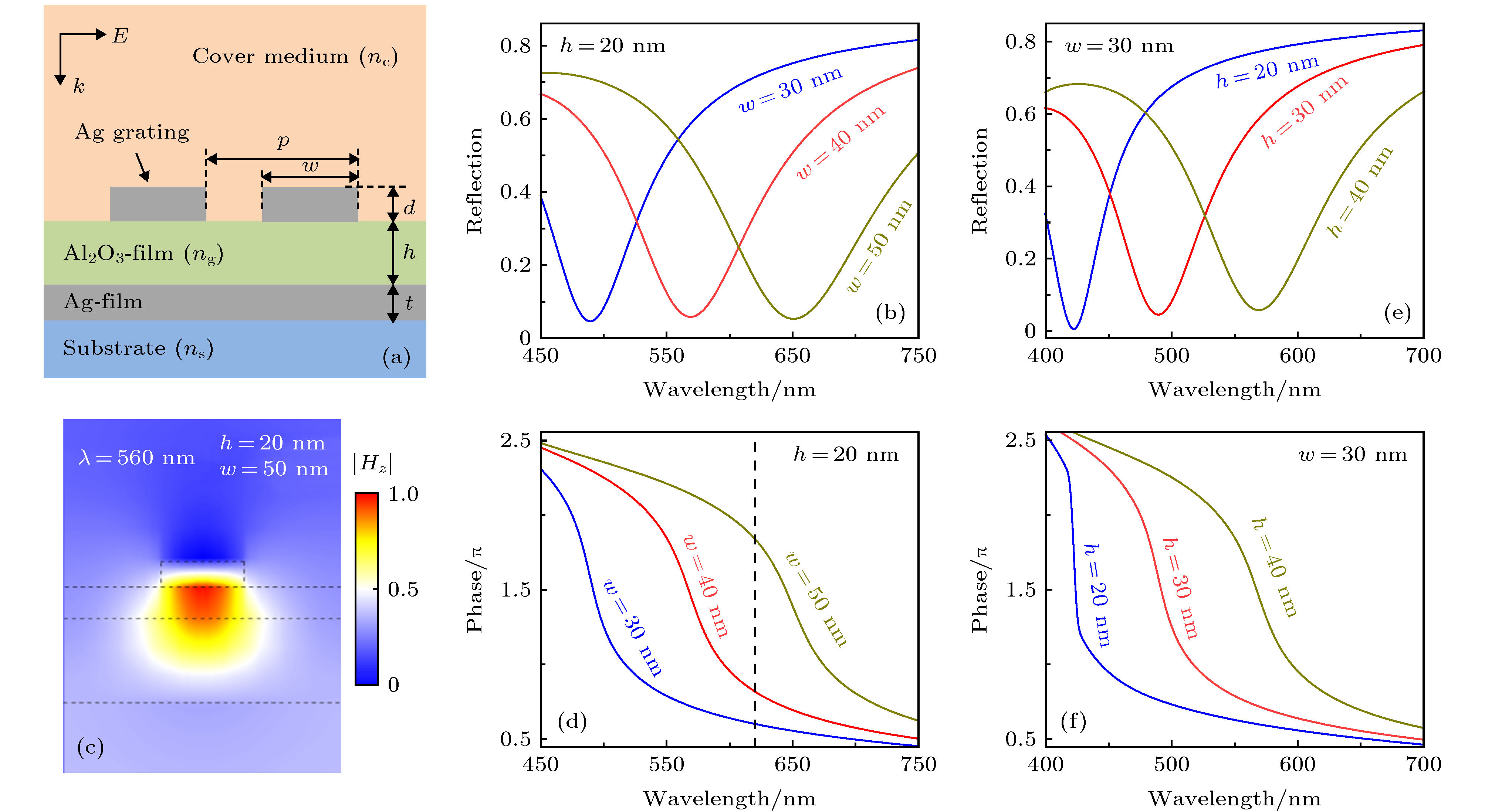
图 1 (a)银光栅-氧化铝介质层-银薄膜构成的超表面结构示意图, 其中银薄膜厚度、银光栅周期和厚度分别固定为t = 30 nm, p = 150 nm和d = 10 nm; (b), (d)氧化铝层厚度h = 20 nm银光栅同宽度时超表面的反射谱和反射位相; (c)光栅宽度w = 50 nm和氧化铝层厚度h = 20 nm的超表面在共振时的磁场分布图; (e), (f)银光栅宽度w = 30 nm氧化铝层厚度不同时超表面的反射谱和反射位相
Figure 1. (a) A schematic diagram of metasurface consisting of silver grating, alumina dielectric layer and silver film, in which the thickness of silver film, the period and thickness of silver grating are fixed at t = 30 nm, P = 150 nm and d = 10 nm, respectively; (b), (d) the thickness of alumina layer is h = 20 nm, and the reflection spectrum and phase of metasurface at different width of silver grating; (c) the magnetic field distribution of metasurface at resonance with grating width w = 50 nm and alumina layer thickness h = 20 nm; (e), (f) with grating width w = 30 nm and different thickness of alumina layer have reflected spectra and phases on the metasurface.
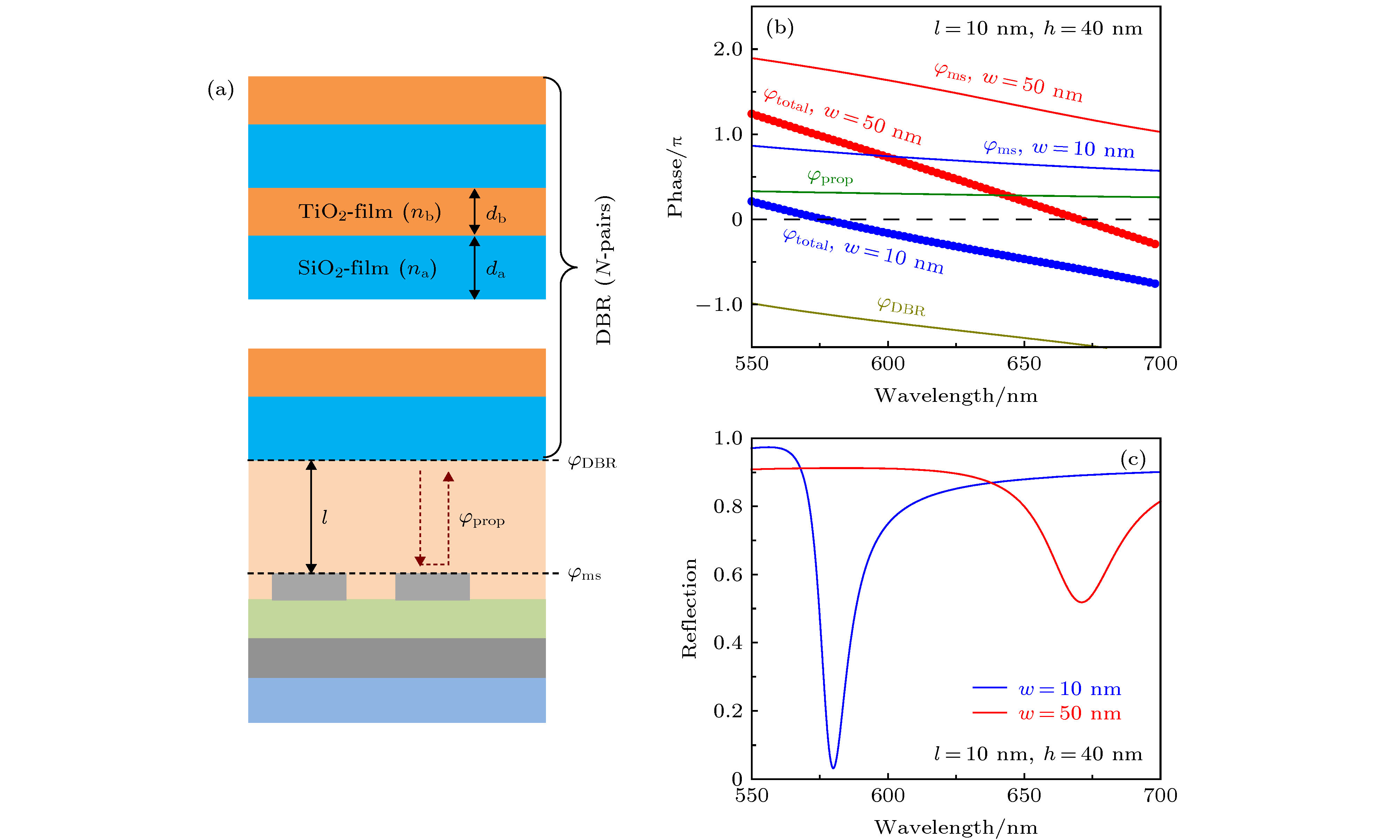
图 2 (a)由超表面-介质间隔层-DBR构成的Tamm等离激元微腔结构示意图. DBR由8对二氧化硅和二氧化钛多层介质膜组成, 其中二氧化硅和二氧化钛的折射率为n a = 1.45和n b = 2.4, 厚度为d a = 103.5 nm和d b = 62.5 nm; 介质间隔层厚度为l, 折射率与图1(a)中超表面结构的包覆层折射率相同, 超表面的结构参数与图1(a)中所展示的相同. φDBR和φmetal分别是光在DBR的表面和超表面结构的表面反射引起的位相变化, φ prop代表光在介质间隔层中的传播位相; (b)固定介质间隔层厚度为l = 10 nm, 超表面中氧化铝层厚度为h = 40 nm, 银光栅宽度为w = 10 nm和50 nm两种情况下所获得的φms以及φDBR, φprop, 总位相φtotal随波长的变化关系. 水平虚线代表相位为0; (c) l = 10 nm, h = 40 nm以及w = 10 nm和50 nm条件下的超表面-介质间隔层-DBR结构的反射谱
Figure 2. (a) A schematic diagram of the structure of a Tamm plasmon microcavity consisting of metasurface-dielectric spacer-DBR. DBR consists of 8 pairs of silica and titanium dioxide multilayer dielectric films, in which the refractive index of silica is n a = 1.45, the refractive index of titanium dioxide is n b = 2.4, and the thickness of silica and titanium dioxide in each layer is d a = 103.5 nm and d b = 62.5 nm. The thickness of the dielectric spacer is l, and the refractive index is the same as that of the cladding layer of the metasurface structure in Fig. 1(a). The structural parameters of the metasurface are the same as those shown in Fig. 1(a). The phase transitions of φDBR and φmetal are caused by the reflection of light on the surface of DBR and metasurface structure respectively. φprop represents the phase of light propagating in the dielectric spacer; (b) the thickness of fixed dielectric spacer is l = 10 nm, the thickness of alumina layer in metasurface is h = 40 nm, and the width of silver grating is w = 10 nm and 50 nm. In both cases, the relationship between wavelength and the obtained φms, φDBR, φprop and total phase φtotal is obtained. The horizontal dashed line represents the phase of 0; (c) reflectance spectra of metasurface-dielectric spacer-DBR structures at l = 10 nm, h = 40 nm and w = 10 nm and 50 nm.

图 3 (a)金属薄膜-介质间隔层-DBR结构中Tamm等离激元模式的共振波长随介质间隔层厚度l的变化关系. 超表面-介质间隔层-DBR结构中固定介质间隔层厚度l = 10 nm和氧化铝层厚度h = 30 nm时Tamm等离激元模式共振波长随银光栅宽度w的变化关系以及l = 10 nm和w = 40 nm时Tamm等离激元模式的共振波长随氧化铝层厚度h的变化关系; (b)介质间隔层厚度固定为l = 10 nm时, 不同的氧化铝层厚度h和银光栅宽度w的参数组合情况下超表面-介质间隔层-DBR结构的反射光谱
Figure 3. (a) The variation of Tamm plasmon mode wavelength with the thickness of dielectric spacer l in metal film-dielectric spacer-DBR structure, the variation of Tamm plasmon mode wavelength with the width of silver grating w when the thickness of fixed dielectric spacer l = 10 nm and alumina layer h = 30 nm in metasurface-dielectric spacer-DBR structure, and fixed l = 10 nm and w = 40 nm, the Tamm plasmon mode wavelength varies with the thickness of alumina layer h; (b) reflectance spectra of metasurface-dielectric spacer-DBR structure with different thickness of alumina and width of silver grating w when the thickness of dielectric spacer is fixed at l = 10 nm.

图 4 (a)和(b)分别为共振波长位于620 nm的常规金属薄膜-介质间隔层-DBR结构和超表面-介质间隔层-DBR结构的反射谱和吸收谱; (c)和(d)分别为有超表面的和常规的Tamm等离激元微腔结构所支持的Tamm等离激元模式的电场分布图. 左侧为结构示意图, 水平虚线代表二维激子材料在结构中放置的位置; (e)和(f)分别为两种Tamm等离激元微腔中加入二维激子材料后的反射谱和吸收谱
Figure 4. (a) and (b) are the reflection and absorption spectra of the conventional metal film-dielectric spacer-DBR structure and the metasurface-dielectric spacer-DBR structure with resonant wavelength at 620 nm, respectively; (c) and (d) electric field distributions of Tamm plasmon modes supported by metasurface and conventional Tamm plasmon microcavities, respectively. On the left is a structural sketch. The horizontal dashed line represents the position of the two-dimensional exciton material in the structure; (e) and (f) are the reflection and absorption spectra of two kinds of Tamm plasmon microcavities with two-dimensional exciton materials.
-
[1] Gramotnev D K, Bozhevolnyi S I 2010 Nat. Photonics 4 83
Google Scholar
[2] Schuller J A, Barnard E S, Cai W, Jun Y C, White J S, Brongersma M L 2010 Nat. Mater. 9 193
Google Scholar
[3] McFarland A D, Van Duyne R P 2013 Nano Lett. 3 1057
[4] Kinkhabwala A, Yu Z, Fan S, Avlasevich Y, Müllen K, Moerner W E 2009 Nat. Photonics 3 654
Google Scholar
[5] Schietinger S, Barth M, Aichele T, Benson O 2009 Nano Lett. 9 1694
Google Scholar
[6] Xu H, Bjerneld E J, Käll M, Börjesson L 1999 Phys. Rev. Lett. 83 4357
Google Scholar
[7] Vasa P, Wang W, Pomraenke R, Lammers M, Maiuri M, Manzoni C, Cerullo G, Lienau C 2013 Nat. Photonics 7 128
Google Scholar
[8] Santhosh K, Bitton O, Chuntonov L, Haran G 2016 Nat. Commun. 7 11823
Google Scholar
[9] Shi L, Hakala T K, Rekola H T, Martikainen J P, Moerland R J, Törmä P 2014 Phys. Rev. Lett. 112 153002
Google Scholar
[10] Ramezani M, Le-Van Q, Halpin A, Rivas J G 2018 Phys. Rev. Lett. 121 243904
Google Scholar
[11] Bellessa J, Symonds C, Vynck K, Lemaitre A, Brioude A, Beaur L, Plenet J C, Viste P, Fellbacq D, Cambrll E, Valvin P 2009 Phys. Rev. B 80 033303
Google Scholar
[12] 赵泽宇, 刘晋侨, 李爱, 武徐颖 2016 物理学报 65 231101
Google Scholar
Zhao Z Y, Liu J Q, Li A W, Xu X Y 2016 Acta Phys. Sin. 65 231101
Google Scholar
[13] Coles D M, Yang Y, Wang Y, Grant R T, Taylor R A, Saikin S K, Aspuru-Guzik A, Lidzey D G, Tang J K, Smith J M 2014 Nat. Commun. 5 5561
Google Scholar
[14] Todorov Y, Andrews A M, Sagnes I, Colombelli R, Klang P, Strasser G, Sirtori C 2009 Phys. Rev. Lett. 102 186402
Google Scholar
[15] Schwartz T, Hutchison J A, Genet C, Ebbesen T W 2011 Phys. Rev. Lett. 106 196405
Google Scholar
[16] Wurdack M, Lundt N, Klaas M, Baumann V, Kavokin A V, Höfling S, Schneider C 2017 Nat. Commun. 8 259
Google Scholar
[17] Lundt N, Klembt S, Cherotchenko E, Betzold S, Iff O, Nalitov A V, Klaas M, Dietrich C P, Kavokin A V, Höfling S, Schneider C 2016 Nat. Commun. 7 13328
Google Scholar
[18] Yu N, Aieta F, Genevet P, Kats M A, Gaburro Z, Capasso F 2012 Nano Lett. 12 6328
Google Scholar
[19] Yu N, Genevet P, Kats M A, Aieta F, Tetienne J P, Capasso F, Gaburro Z 2011 Science 334 333
Google Scholar
[20] Yang Y, Wang W, Moitra P, Kravchenko I I, Briggs D P, Valentine J 2014 Nano Lett. 14 1394
Google Scholar
[21] Jiang S C, Xiong X, Hu Y S, Hu Y H, Ma G B, Peng R W, Sun C, Wang M 2014 Phys. Rev. X 4 021026
[22] Lin D, Fan P, Hasman E, Brongersma M L 2014 Science 345 298
Google Scholar
[23] Zheng G, Mühlenbernd H, Kenney M, Li G, Zentgraf T, Zhang S 2015 Nat. Nanotechnol. 10 308
Google Scholar
[24] Wang S, Wu P C, Su V C, Lai Y C, Chen M K, Kuo H Y, Chen B H, Huang T T, Wang J H, Lin R M, Kuan C H, Li T, Wang Z, Tsai D P 2018 Nat. Nanotechnol. 13 227
Google Scholar
[25] Deng Z L, Deng J, Zhuang X, Wang S, Li K, Wang Y, Chi Y, Ye X, Xu J, Wang G P, Zhao R, Wang X, Cao Y, Cheng X, Li G, Li X 2018 Nano Lett. 18 2885
Google Scholar
[26] Wang S, Li F, Deng J, Ye X, Deng Z L, Cao Y, Guan B O, Li G, Li X 2019 J. Phys. D: Appl. Phys. 52 324002
Google Scholar
[27] Blaber M G, Arnold M D, Ford M J 2009 J. Phys. Chem. C 113 3041
[28] Dai Y, Ren W, Cai H, Ding H, Pan N, Wang X 2014 Opt. Express 22 7465
Google Scholar
[29] Liu W, Lee B, Naylor C H, Ee H S, Park J, Johnson A C, Agarwal R 2016 Nano Lett. 16 1262
Google Scholar
[30] Li Y, Chernikov A, Zhang X, Rigosi A, Hill H M, van der Zande A M, Chenet D A, Shih E M, Hone J, Heinz T F 2014 Phys. Rev. B 90 205422
Google Scholar

 DownLoad:
Catalog
Metrics
- Abstract views: 22752
- PDF Downloads: 589
- Cited By: 0
