


-
Near-field imaging and active control of excitation efficiency of femtosecond propagating surface plasmon (fs-PSP) are the prerequisites for its application. Here, we perform near-field imaging of fs-PSP excited at the trench etched on silver nano-film by using photoemission electron microscopy (PEEM). As an excellent near-field microscopy technique of in situ imaging with a high spatial resolution (< 20 nm), it needs neither molecular reporters nor scanning probes as required in nonlinear fluorescence microscopy in nonlinear fluorescence microscopy or scanning near-field optical microscopy, both of which may potentially bias PSP derived from such measurements. The period of the interference patterns induced by the incident femtosecond laser and the laser-induced fs-PSP and the wavelength of fs-PSP in a range of 720–900 nm of the incident laser wavelength are systematically measured. The fringe period of the interference pattern between fs-PSP and the incident laser is a range of 5.9–7.7 µm, and the wavelength of fs-PSP is in a range of 700–879 nm. The experimental results are consistent with the theoretical simulation results. Furthermore, we demonstrate that the excitation efficiency of fs-PSP can be actively controlled by adjusting the polarization direction of the incident laser in the femtosecond pump-probe experiments. Specifically, it is found that when the incident laser is polarized to 0° (p-polarization light), the excitation efficiency of PSP reaches a maximum value, and when the incident light is polarized to 90° (s-polarization light), the excitation efficiency of fs-PSP is the lowest. Unlike the simulation result by the finite difference time domain (FDTD) method, a plateau area of the intensity of the photoemission signal with the polarization direction of the incident laser appears in the femtosecond pump-probe experiment. This phenomenon is attributed to the background noise of the detection laser that masks the change of the fs-PSP excitation efficiency. In a word, this research realizes the experimental measurement of the basic parameters of fs-PSP and the manipulation of fs-PSP excitation efficiency by adjusting the polarization angle of the incident laser. This research lays a foundation for realizing the engineering manipulation of fs-PSP excitation efficiency and optimizing the performance of plasmonic devices.
-
Keywords:
- photoemission electron microscopy /
- femtosecond propagating surface plasmon /
- near-field imaging /
- regulation of excitation efficiency
[1] Gramotnev D K, Bozhevolnyi S I 2010 Nat. Photonics 4 83
 Google Scholar
[2] Ozbay E 2006 Science 311 189
Google Scholar
[3] Wei H, Pan D, Zhang S P, Li Z P, Li Q, Liu N, Xu H X, Wang W H 2018 Chem. Rev. 118 2882
Google Scholar
[4] Gong Y, Joly A G, Hu D, El-Khoury P Z, Hess W P 2015 Nano Lett. 15 3472
Google Scholar
[5] Pyayt A L, Wiley B, Xia Y, Chen A, Dalton L 2008 Nat. Nanotechnol. 3 660
Google Scholar
[6] Li X, Huang L, Tan Q, Bai B, Jin G 2011 Opt. Express 19 6541
Google Scholar
[7] Sumimura A, Ota M, Nakayama K, Ito M, Ishii Y, Fukuda M 2016 IEEE Photonics Technol. Lett. 28 2419
Google Scholar
[8] Chang K W, Huang C C 2016 Sci. Rep. 6 19609
Google Scholar
[9] Hu T, Qiu H, Zhang Z, Guo X, Liu C, Rouifed M S, Littlejohns C G, Reed G T, Wang H 2016 IEEE Photonics J. 8 4802209
Google Scholar
[10] Lemke C, Schneider C, Leißner T, Bayer D, Radke J W, Fischer A, Melchior P, Evlyukhin A B, Chichkov B N, Reinhardt C, Bauer M, Aeschlimann M 2013 Nano Lett. 13 1053
Google Scholar
[11] Bettina F, Philip K, Daniel P, Grisha S, Meir O, Fu L W, Thomas W, Michael H H, Timothy J D, Frank-J M Z H, Harald G 2017 Sci. Adv. 3 e1700721
Google Scholar
[12] Zu S, Han T Y, Jiang M L, Liu Z X, Jiang Q, Lin F, Zhu X, Fang Z Y 2019 Nano Lett. 19 775
Google Scholar
[13] Zu S, Han T Y, Jiang M L, Lin F, Zhu X, Fang Z Y 2018 ACS Nano 12 3908
Google Scholar
[14] Han T Y, Zu S, Li Z W, Jiang M L, Zhu X, Fang Z Y 2018 Nano Lett. 18 567
Google Scholar
[15] Liu Z X, Jiang M L, Hu Y L, Lin F, Shen B, Zhu X, Fang Z Y 2018 Opto-Electron. 1 180007
Google Scholar
[16] EL-Khoury P Z, Abellan P, Gong Y, Hage F S, Cottom J, Joly A G, Brydson R, Ramasse Q M, Hess W P 2016 The Anakyst 141 3562
Google Scholar
[17] Wild B, Cao L, Sun Y, Khanal B P, Zubarev E R, Gray S K, Pelton M, Scherer N F 2012 ACS Nano 6 472
Google Scholar
[18] Liu X J, Wang Y, Potma E O 2012 Appl. Phys. Lett. 101 081116
Google Scholar
[19] Zhang W H, Fang Z Y, Zhu X 2017 Chem. Rev. 117 5095
Google Scholar
[20] Yin L L, Vlasko-Vlasov V K, Pearson J, Hiller J M, Hua J, Welp U, Brown D E, Kimball C W 2005 Nano Lett. 5 1399
Google Scholar
[21] Fang Z Y, Zhu X 2013 Adv. Mater. 25 3840
Google Scholar
[22] Kubo A, Pontius N, Petek H 2007 Nano Lett. 7 470
Google Scholar
[23] Sun Q, Zu S, Misawa H 2020 J. Chem. Phys. 153 120902
Google Scholar
[24] Dąbrowski M, Dai Y N, Petek H 2017 J. Phys. Chem. Lett. 8 4446
Google Scholar
[25] Ditlbacher H, Krenn J R, Hohenau A, Leitner A, Aussenegg F R 2003 Appl. Phys. Lett. 83 3665
Google Scholar
[26] Radko I P, Bozhevolnyi S I, Brucoli G, Martı′n-Moreno L, Garcıá-Vidal F G, Boltaseva A 2008 Phys. Rev. B 78 115115
Google Scholar
[27] Baudrion A L, León-Pérez F, Mahboub O, Hohenau A, Ditlbacher H, Garcıá-Vidal F J, Dintinger J, Ebbesen T W, Martı′n-Moreno L, R.Krenn J 2008 Opt. Express 16 3420
Google Scholar
[28] Lu J, Petre C, Yablonovitch E, Conway J 2007 J. Opt. Soc. Am. B 24 2268
Google Scholar
[29] Klick A, Cruz S L, Lemke C, Großmann M, Beyer H, Fiutowski J, Rubahn H G, Mendez E R, Bauer M 2016 Appl. Phys. B 122 79
Google Scholar
[30] Zhang L X, Kubo A, Wang L, Petek H, Seideman T 2011 Phys. Rev. B 84 245442
Google Scholar
[31] Buckanie N M, Kirschbaum P, Sindermann S, Meyer zu J, Heringdorf F 2013 Ultramicroscopy 130 49
Google Scholar
[32] Gong Y, Joly A G, EI-Khoury P Z, Hess W P 2017 J. Phys. Chem. Lett. 8 49
Google Scholar
[33] Qin Y L, Song X W, Ji B Y, Xu Y, Lin J Q 2019 Opt. Lett. 44 2935
Google Scholar
-
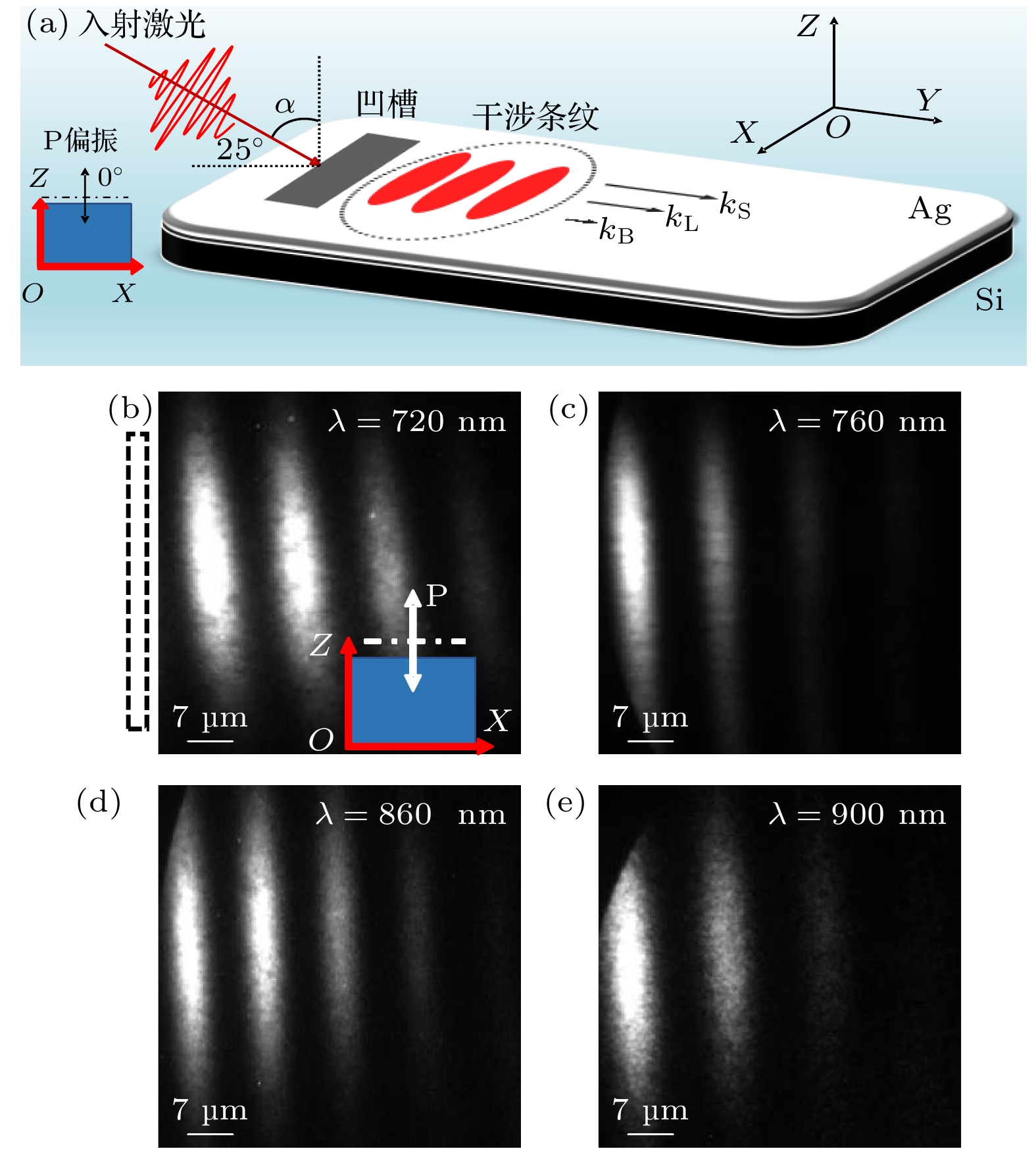
图 1 (a)激发fs-PSP的实验示意图; (b)−(e)分别表示入射激光波长为720, 760, 860 和900 nm时的PEEM图像
Figure 1. (a) Schematic diagram of the experiment of exciting fs-PSP; (b)−(e) the PEEM images when the incident laser wavelength is 720 nm, 760 nm, 860 nm and 900 nm, respectively.
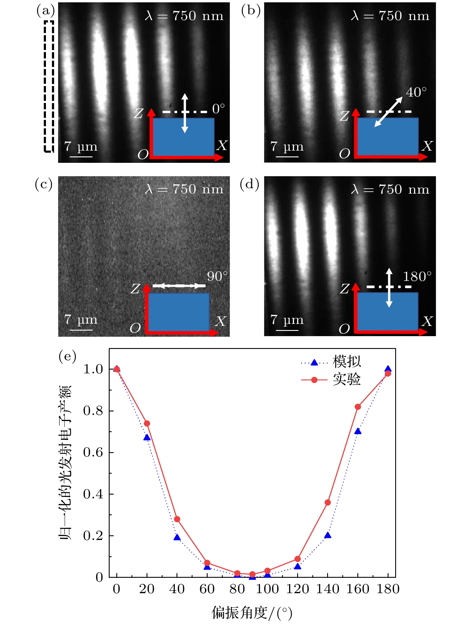
图 2 (a)−(d) 750 nm入射激光, 随偏振角度变化的PEEM图像; (e) fs-PSP归一化的光发射电子产额随入射激光偏振角度变化的模拟和实验曲线
Figure 2. (a)−(d) The PEEM images of the incident laser at 750 nm, changing with the polarization angle; (e) simulation and experimental curves of fs-PSP normalized light emission electron yield with incident laser polarization angle.
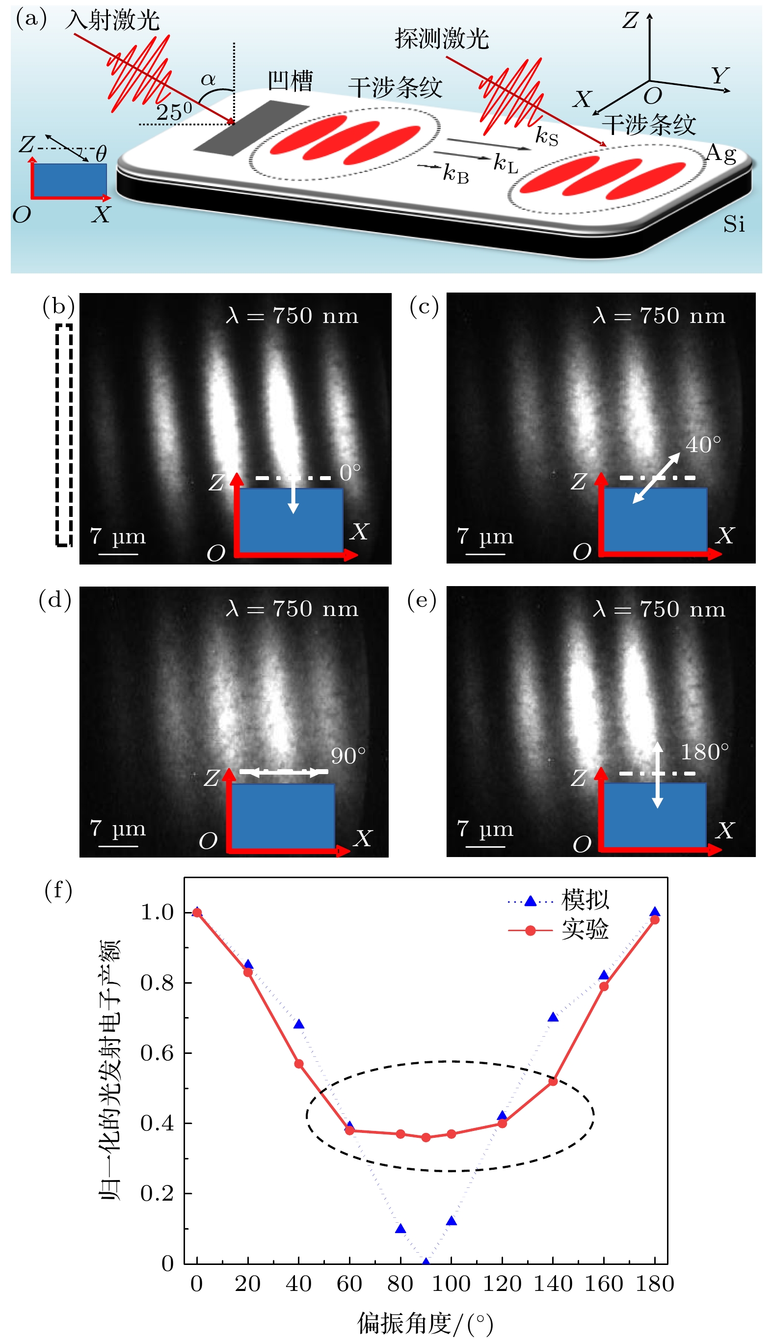
图 3 (a)飞秒双光束泵浦-探测实验示意图; (b)−(e) 750 nm入射激光, 在探测光辐照区域, 随偏振角度变化的PEEM图像; (f) fs-PSP归一化的光发射电子产额随入射激光偏振角度变化的模拟和实验曲线
Figure 3. (a) Schematic diagram of femtosecond dual-beam pumping-detection experiment; (b)−(e) the PEEM images of the incident laser at 750 nm in the area irradiated by the probe light with the polarization angle; (f) the simulation and experimental curves of fs-PSP normalized light emission electron yield with the incident laser polarization angle.
表 1 fs-PSP的波长及干涉条纹周期随入射激光波长改变的数值
Table 1. The value of fs-PSP's wavelength and interference fringe period changing with the incident laser wavelength.
入射光波长 $ {\lambda }_{\rm{L}}/ $nm 720 740 760 780 800 820 840 860 880 900 fs-PSP拍频周期 $ {\lambda }_{\rm{B}}/ $µm 5.9 6.1 6.6 6.7 7.0 7.1 7.2 7.3 7.5 7.7 fs-PSP波长的理论值$ {\lambda }_{{\rm{s}}{\rm{s}}}/ $nm 706 726 746 766 785 805 824 844 864 883 fs-PSP波长实验测得值$ {\lambda }_{{\rm{s}}{\rm{m}}}/ $nm 700 720 744 765 784 803 821 840 859 879  DownLoad: CSV
-
[1] Gramotnev D K, Bozhevolnyi S I 2010 Nat. Photonics 4 83
Google Scholar
[2] Ozbay E 2006 Science 311 189
Google Scholar
[3] Wei H, Pan D, Zhang S P, Li Z P, Li Q, Liu N, Xu H X, Wang W H 2018 Chem. Rev. 118 2882
Google Scholar
[4] Gong Y, Joly A G, Hu D, El-Khoury P Z, Hess W P 2015 Nano Lett. 15 3472
Google Scholar
[5] Pyayt A L, Wiley B, Xia Y, Chen A, Dalton L 2008 Nat. Nanotechnol. 3 660
Google Scholar
[6] Li X, Huang L, Tan Q, Bai B, Jin G 2011 Opt. Express 19 6541
Google Scholar
[7] Sumimura A, Ota M, Nakayama K, Ito M, Ishii Y, Fukuda M 2016 IEEE Photonics Technol. Lett. 28 2419
Google Scholar
[8] Chang K W, Huang C C 2016 Sci. Rep. 6 19609
Google Scholar
[9] Hu T, Qiu H, Zhang Z, Guo X, Liu C, Rouifed M S, Littlejohns C G, Reed G T, Wang H 2016 IEEE Photonics J. 8 4802209
Google Scholar
[10] Lemke C, Schneider C, Leißner T, Bayer D, Radke J W, Fischer A, Melchior P, Evlyukhin A B, Chichkov B N, Reinhardt C, Bauer M, Aeschlimann M 2013 Nano Lett. 13 1053
Google Scholar
[11] Bettina F, Philip K, Daniel P, Grisha S, Meir O, Fu L W, Thomas W, Michael H H, Timothy J D, Frank-J M Z H, Harald G 2017 Sci. Adv. 3 e1700721
Google Scholar
[12] Zu S, Han T Y, Jiang M L, Liu Z X, Jiang Q, Lin F, Zhu X, Fang Z Y 2019 Nano Lett. 19 775
Google Scholar
[13] Zu S, Han T Y, Jiang M L, Lin F, Zhu X, Fang Z Y 2018 ACS Nano 12 3908
Google Scholar
[14] Han T Y, Zu S, Li Z W, Jiang M L, Zhu X, Fang Z Y 2018 Nano Lett. 18 567
Google Scholar
[15] Liu Z X, Jiang M L, Hu Y L, Lin F, Shen B, Zhu X, Fang Z Y 2018 Opto-Electron. 1 180007
Google Scholar
[16] EL-Khoury P Z, Abellan P, Gong Y, Hage F S, Cottom J, Joly A G, Brydson R, Ramasse Q M, Hess W P 2016 The Anakyst 141 3562
Google Scholar
[17] Wild B, Cao L, Sun Y, Khanal B P, Zubarev E R, Gray S K, Pelton M, Scherer N F 2012 ACS Nano 6 472
Google Scholar
[18] Liu X J, Wang Y, Potma E O 2012 Appl. Phys. Lett. 101 081116
Google Scholar
[19] Zhang W H, Fang Z Y, Zhu X 2017 Chem. Rev. 117 5095
Google Scholar
[20] Yin L L, Vlasko-Vlasov V K, Pearson J, Hiller J M, Hua J, Welp U, Brown D E, Kimball C W 2005 Nano Lett. 5 1399
Google Scholar
[21] Fang Z Y, Zhu X 2013 Adv. Mater. 25 3840
Google Scholar
[22] Kubo A, Pontius N, Petek H 2007 Nano Lett. 7 470
Google Scholar
[23] Sun Q, Zu S, Misawa H 2020 J. Chem. Phys. 153 120902
Google Scholar
[24] Dąbrowski M, Dai Y N, Petek H 2017 J. Phys. Chem. Lett. 8 4446
Google Scholar
[25] Ditlbacher H, Krenn J R, Hohenau A, Leitner A, Aussenegg F R 2003 Appl. Phys. Lett. 83 3665
Google Scholar
[26] Radko I P, Bozhevolnyi S I, Brucoli G, Martı′n-Moreno L, Garcıá-Vidal F G, Boltaseva A 2008 Phys. Rev. B 78 115115
Google Scholar
[27] Baudrion A L, León-Pérez F, Mahboub O, Hohenau A, Ditlbacher H, Garcıá-Vidal F J, Dintinger J, Ebbesen T W, Martı′n-Moreno L, R.Krenn J 2008 Opt. Express 16 3420
Google Scholar
[28] Lu J, Petre C, Yablonovitch E, Conway J 2007 J. Opt. Soc. Am. B 24 2268
Google Scholar
[29] Klick A, Cruz S L, Lemke C, Großmann M, Beyer H, Fiutowski J, Rubahn H G, Mendez E R, Bauer M 2016 Appl. Phys. B 122 79
Google Scholar
[30] Zhang L X, Kubo A, Wang L, Petek H, Seideman T 2011 Phys. Rev. B 84 245442
Google Scholar
[31] Buckanie N M, Kirschbaum P, Sindermann S, Meyer zu J, Heringdorf F 2013 Ultramicroscopy 130 49
Google Scholar
[32] Gong Y, Joly A G, EI-Khoury P Z, Hess W P 2017 J. Phys. Chem. Lett. 8 49
Google Scholar
[33] Qin Y L, Song X W, Ji B Y, Xu Y, Lin J Q 2019 Opt. Lett. 44 2935
Google Scholar

 DownLoad:
Catalog
Metrics
- Abstract views: 7772
- PDF Downloads: 101
- Cited By: 0
