


-
The phenomenon of electromagnetically induced transparency (EIT)-like in terahertz (THz) metasurfaces facilitates agile manipulation of electromagnetic wave transmission windows and the deceleration of light, rendering it suitable for applications in modulators, absorbers, slow light devices, and more. Traditional design methodologies focus on the coupling between bright-dark modes and bright-bright modes within the unit cell, leveraging interference cancellation effects to regulate electromagnetic wave transmission. Notably, the periodicity of the array structure also plays a pivotal role in modulating the amplitude and resonance intensity of the transparent window, a phenomenon termed lattice-induced transparency (LIT). In this paper, we introduce a gold nanorod structure and an S-shaped gold split-ring resonator supported on a vanadium dioxide (${\rm{VO}}_{2}$) thin film to investigate LIT. Unlike conventional structures that solely consider single bright-bright or bright-dark mode coupling, our proposed structure incorporates both bright-bright and bright-dark modes coupling. Furthermore, the dark mode in our structure is not a conventional multipolar mode but rather a surface lattice resonance (SLR) arising from the coupling between lattice modes and the localized surface plasmon resonance (LSPR) of the structure itself. Through the analysis of simulated transmission spectra for the individual gold nanorod and S-shaped split-ring structures, we observed that the gold nanorod exhibits LSPR at 0.985 THz, whereas the S-shaped split-ring structure demonstrates LSPR and SLR at 0.51 THz and 1.025 THz, respectively. When combined, these structures form transparent windows with transmission rates of 66.03% and 59.4% at 0.643 THz and 1.01 THz due to the interplay of bright-bright and bright-dark modes coupling. Upon examining the electric field distribution in the x-y plane, we found that the electric field energy is predominantly concentrated on the S-shaped split-ring. To gain deeper insights into each resonance mode, we employed multipolar decomposition to quantify resonance scattering energy. Our findings revealed that both transparent windows are predominantly governed by electric dipole scattering energy. Further investigations showed that as the array structure’s period varies from 60 μm to 95 μm, the lattice mode progressively couples into the high frequency transmission valley (1.031 THz), giving rise to a high frequency hybrid mode (HFHM). The Q value of this mode initially increases and then decreases, peaking at 27 when the period is 84 μm. Similarly, as the period continues to increase, the lattice mode couples into the low frequency resonance valley (0.76 THz), forming a low frequency hybrid mode (LFHM) with a Q value that reaches a maximum of 51 at 115 μm—approximately an order of magnitude higher than that at a period of 60 μm. Additionally, as the periodicity increases, the near field coupling effect between adjacent units diminishes, leading to the gradual disappearance of the two transparent windows. To achieve active control over these transparent windows, we varied the conductivity of ${\rm{VO}}_{2}$ from 20 S/m to 30000 S/m, resulting in a decrease in the transmission amplitudes of the two transparent windows to 37.58% and 3.39%, respectively. Finally, we investigated the slow light effect of the two transparent windows, comparing the maximum group delay between them, which was found to be 8.1 ps. The terahertz metasurface proposed in this study opens up avenues for the design of dynamically tunable sensing and slow light devices in the future. -
Keywords:
- terahertz hybrid metasurface /
- lattice mode /
- lattice-induced transparency /
- quality factor
-
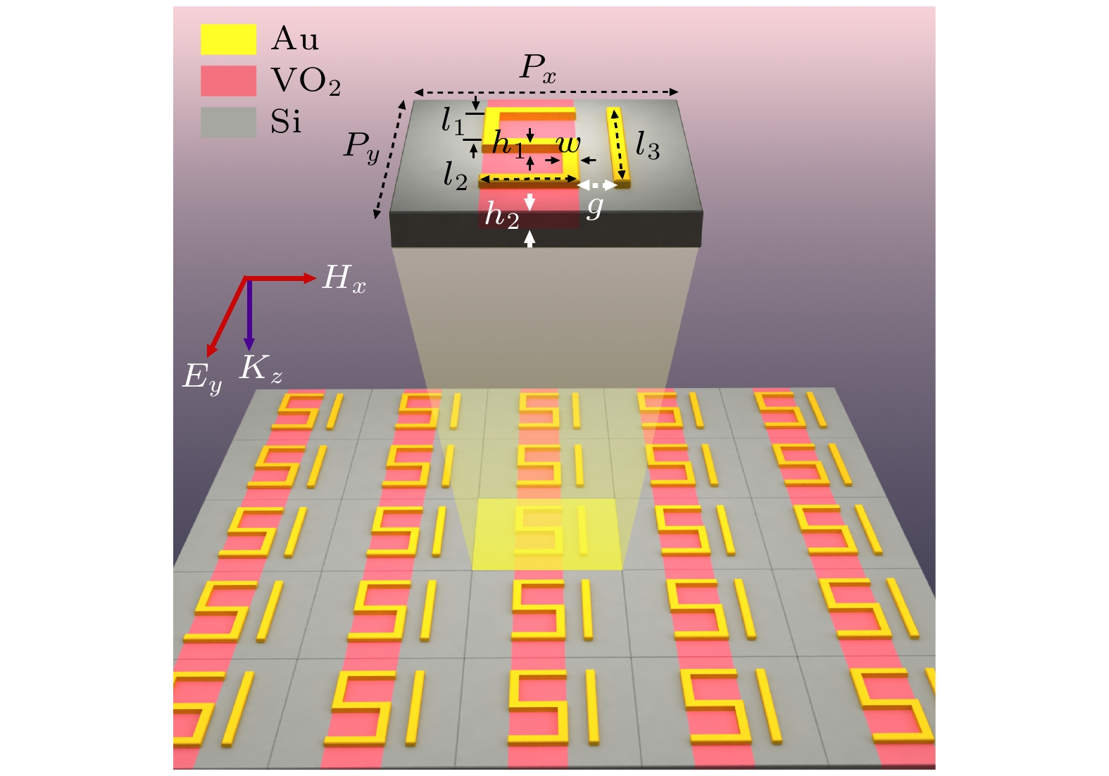
图 1 提出的超表面阵列结构及其单元结构示意图. 其中$ P_{x} $ = $ P_{y} $ = 60 μm, $ l_{1} $ = 17.5 μm, $ l_{2} $ = 25 μm, $ l_{3} $ = 50 μm, w = 5 μm, d = 3 μm, $ h_{1} $ = $ h_{2} $ = 0.2 μm
Figure 1. The proposed metasurface array structure and its unit structure schematic diagram. Among them, $ P_ {x} $ =$ P_ {y} $ = 60 μm, $ l_ {1} $ = 17.5 μm, $ l_ {2} $ = 25 μm, $ l_ {3} $ = 50 μm, w = 5 μm, d = 3 μm, $ h_ {1} $ = $ h_ {2} $ = 0.2 μm.
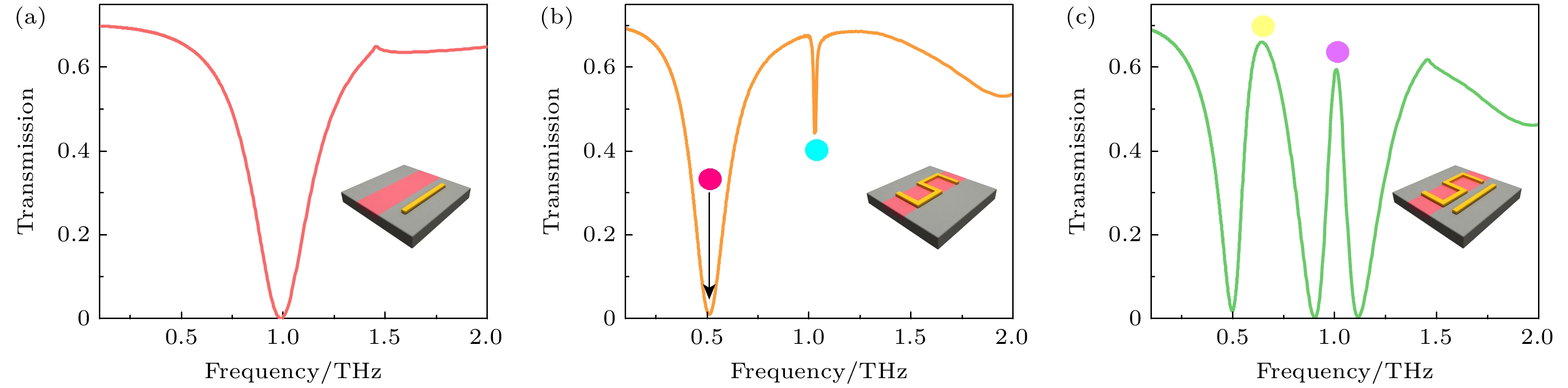
图 2 (a) 金纳米条结构, (b) S型金开口环结构与(c) 组合结构的仿真透射谱; 带颜色的实心圆表示共振位置
Figure 2. (a) Simulation transmission spectra of only the gold nanorod, (b) only the S-shaped split-ring, and (c) both the gold nanorod and the S-shaped split-ring structure. The colored solid circles denote the resonance positions.
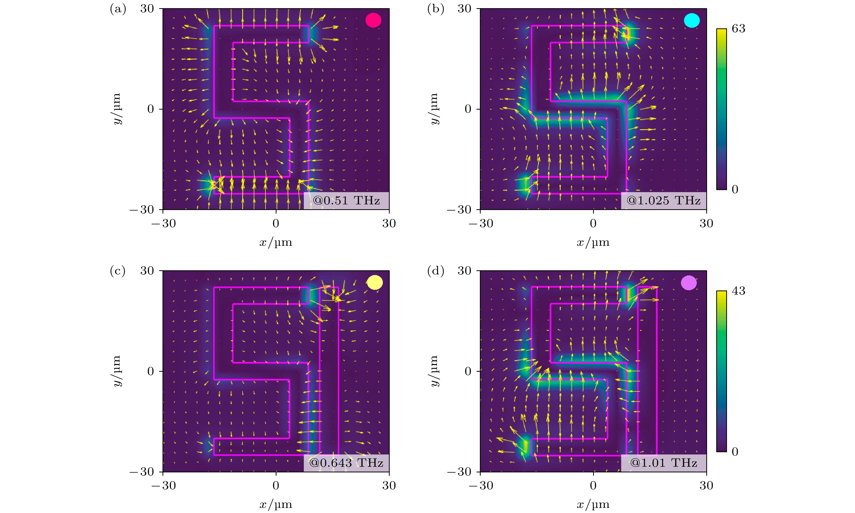
图 3 阵列结构在x-y平面的电场强度分布. S型开口环在(a) 0.51 THz与(b) 1.025 THz处电场分布; (c)(d) 两个透明窗在0.643 THz和1.01 THz处的电场分布; 粉色线为单元结构轮廓, 黄色箭头表示电场方向, 颜色条为共振强度, 这里(a)(b)共用一个颜色条, (c)(d)共用一个颜色条; 带颜色的实心圆对应图2中透射谱的共振位置
Figure 3. The electric field intensity distribution of the proposed array structure in the x-y plane. (a) and (b) show the electric field distribution of the S-shaped split-ring at 0.51 THz and 1.025 THz, respectively; (c) and (d) represent the electric field distribution of the two transparent windows at 0.643 THz and 1.01 THz, respectively. The pink line outlines the unit structure, the yellow arrow denotes the direction of the electric field, and the color bar indicates the resonance intensity. Specifically, (a) and (b) utilize a shared color bar, and similarly, (c) and (d) employ another common color bar. The solid circles with colors correspond to the resonance positions of the transmission spectra in fig. 2.
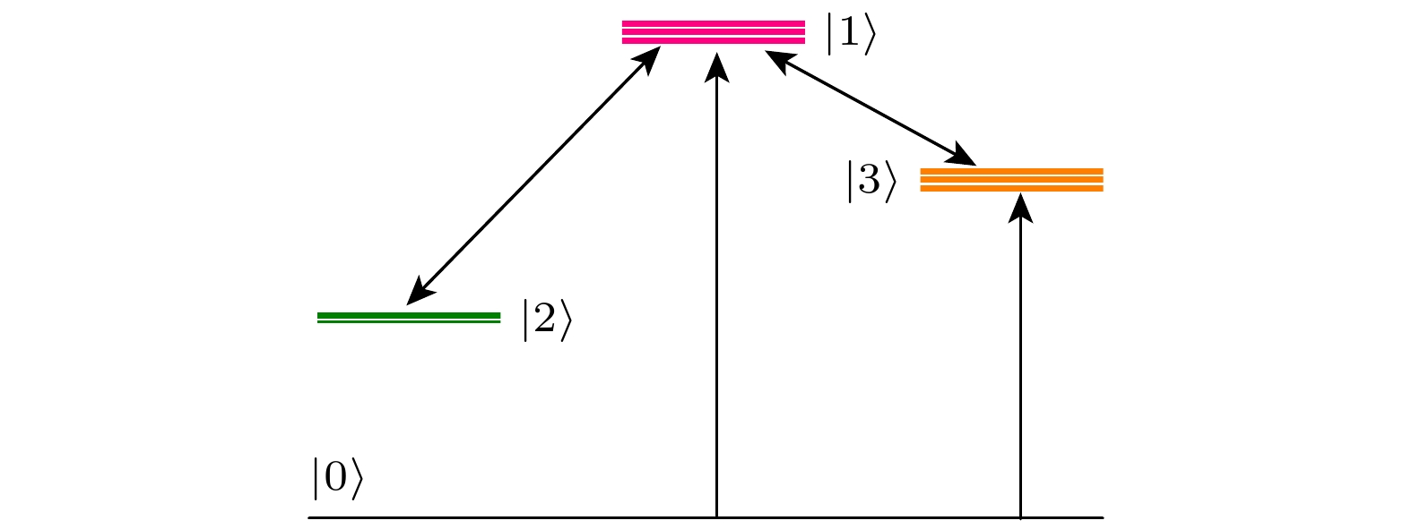
图 4 类EIT效应的四能级系统
Figure 4. The four-level system with EIT-like effect.
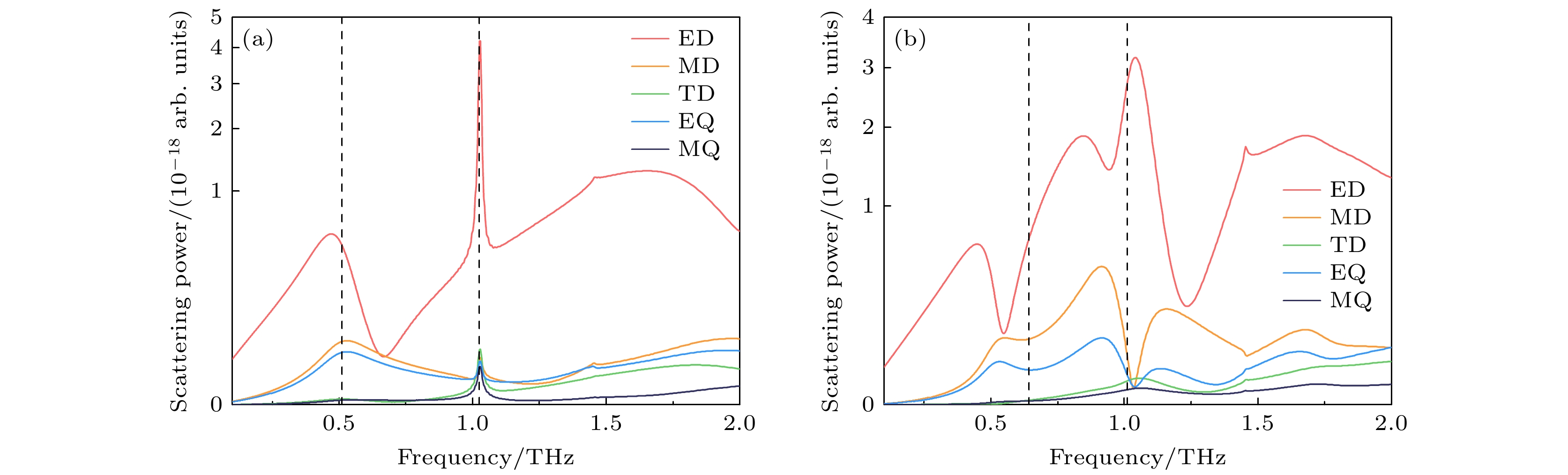
图 5 散射功率谱 (a) S型开口环散射功率谱; (b) 组合结构散射功率谱. ED, MD, TD, EQ, MQ分别表示电偶极子, 磁偶极子, 环偶极子, 电四偶极子, 磁四偶极子; 黑色虚线表示共振位置
Figure 5. scattered power spectra. (a) Scattered power spectra of the S-shaped split-ring; (b) Scattered power spectra of the combined structure. ED, MD, TD, EQ, and MQ denote electric dipole, magnetic dipole, ring dipole, electric quadrupole, and magnetic quadrupole, respectively; black dashed lines denote resonance positions.
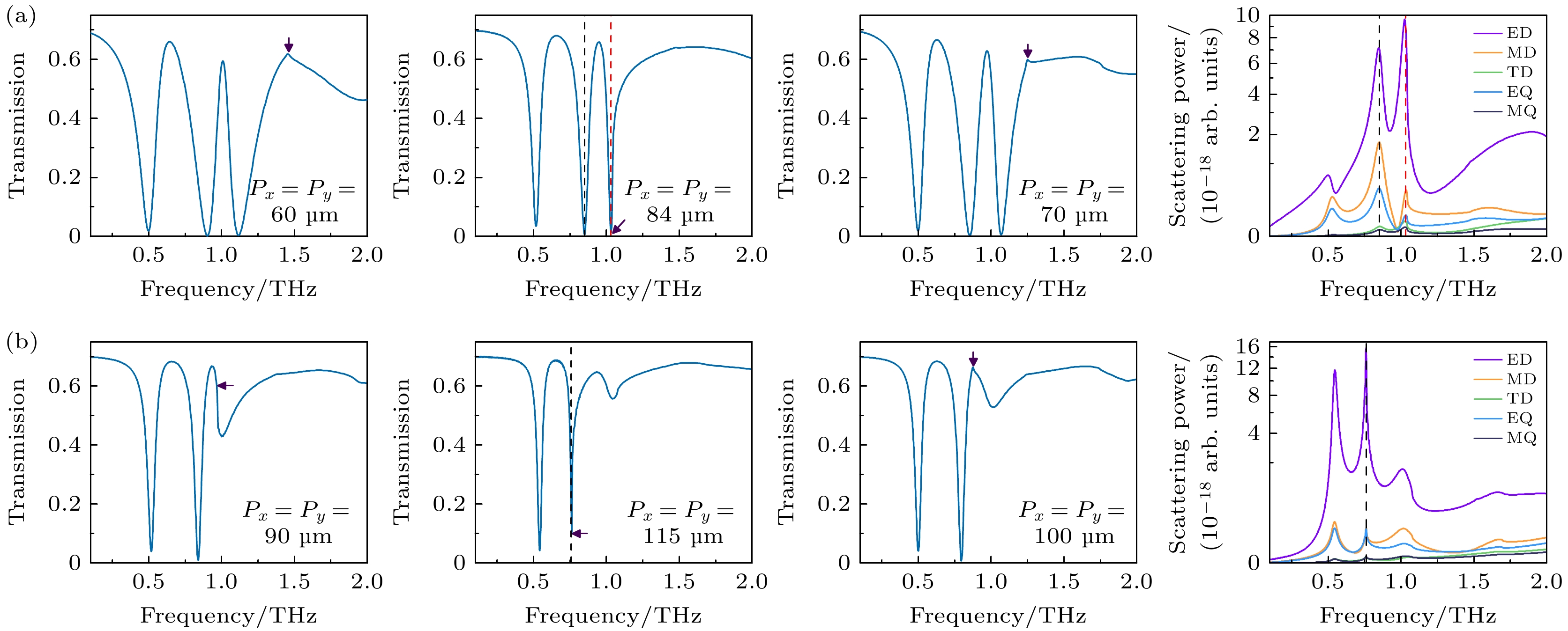
图 6 固定结构参数不变, 周期$ P_x $、$ P_y $从(a) 60 μm变化到84 μm与(b) 90 μm变化到115 μm时, 组合结构的仿真透射谱及其多极子分解散射功率谱. 晶格模式$ f_{{\rm{LM}}(\pm1, 0)} $用黑色三角符号表示, 红色虚线表示HFHM频率位置, 黑色虚线表示LFHM频率位置
Figure 6. With fixed structural parameters, the simulated transmission spectra and multipole decomposition scattering power spectra of the combined structure are presented when the periods $ P_x $ and $ P_y $ are varied from (a) 60 μm to 84 μm and from (b) 90 μm to 115 μm. The lattice mode $ f_{{\rm{LM}}(\pm1, 0)} $ is denoted by black triangular symbols, with the red dashed line indicating the frequency position of HFHM and the black dashed line indicating the frequency position of LFHM.
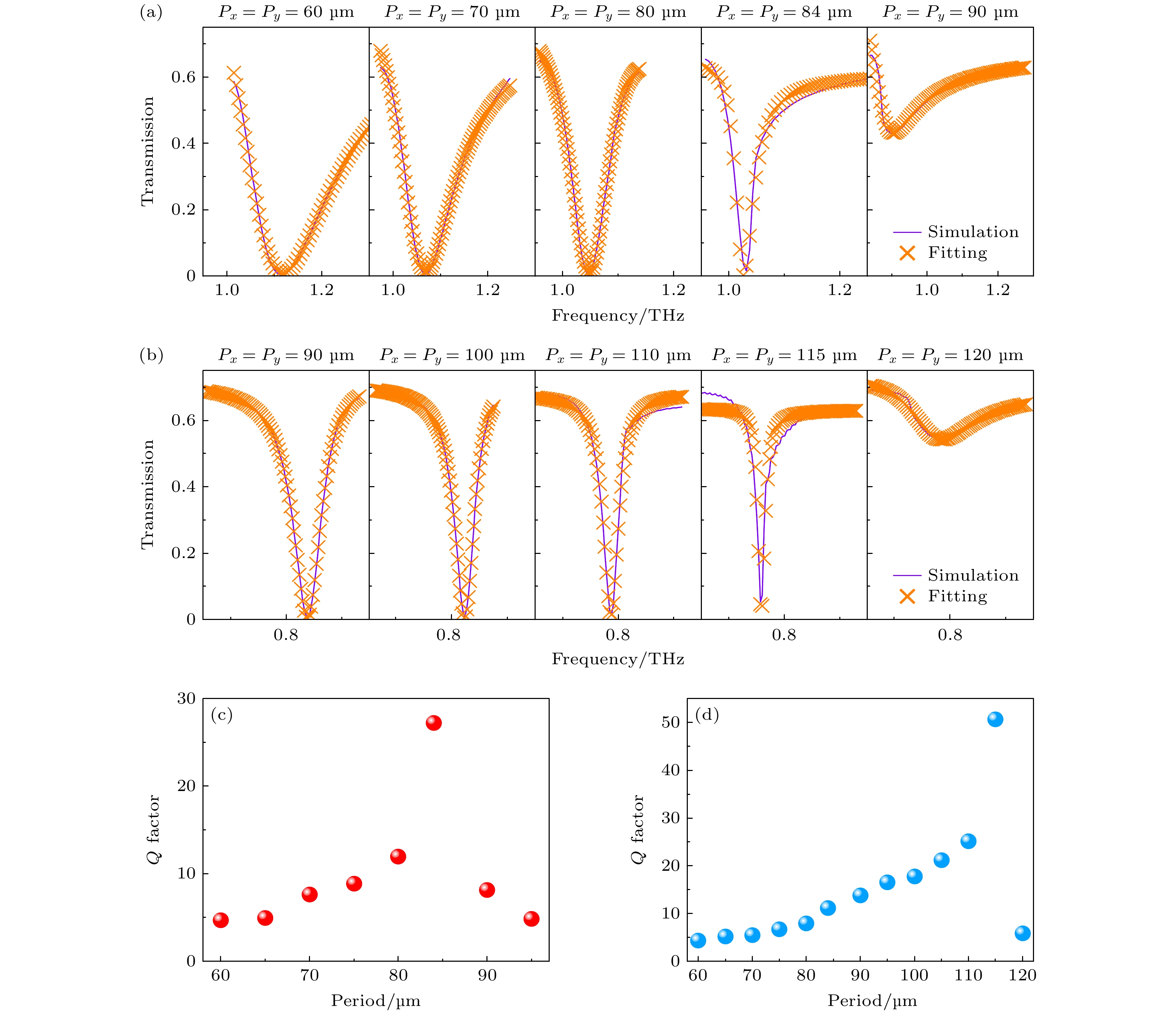
图 7 不同周期下仿真与拟合的(a) HFHM与(b) LFHM透射谱; (c) HFHM与(d) LFHM随着周期的增加品质因子Q变化情况
Figure 7. Simulated transmission spectra of (a) HFHM and (b) LFHM fitted by the Fano formula for varying periods, with (c) HFHM and (d) LFHM quality factor Q variations as the period increases.
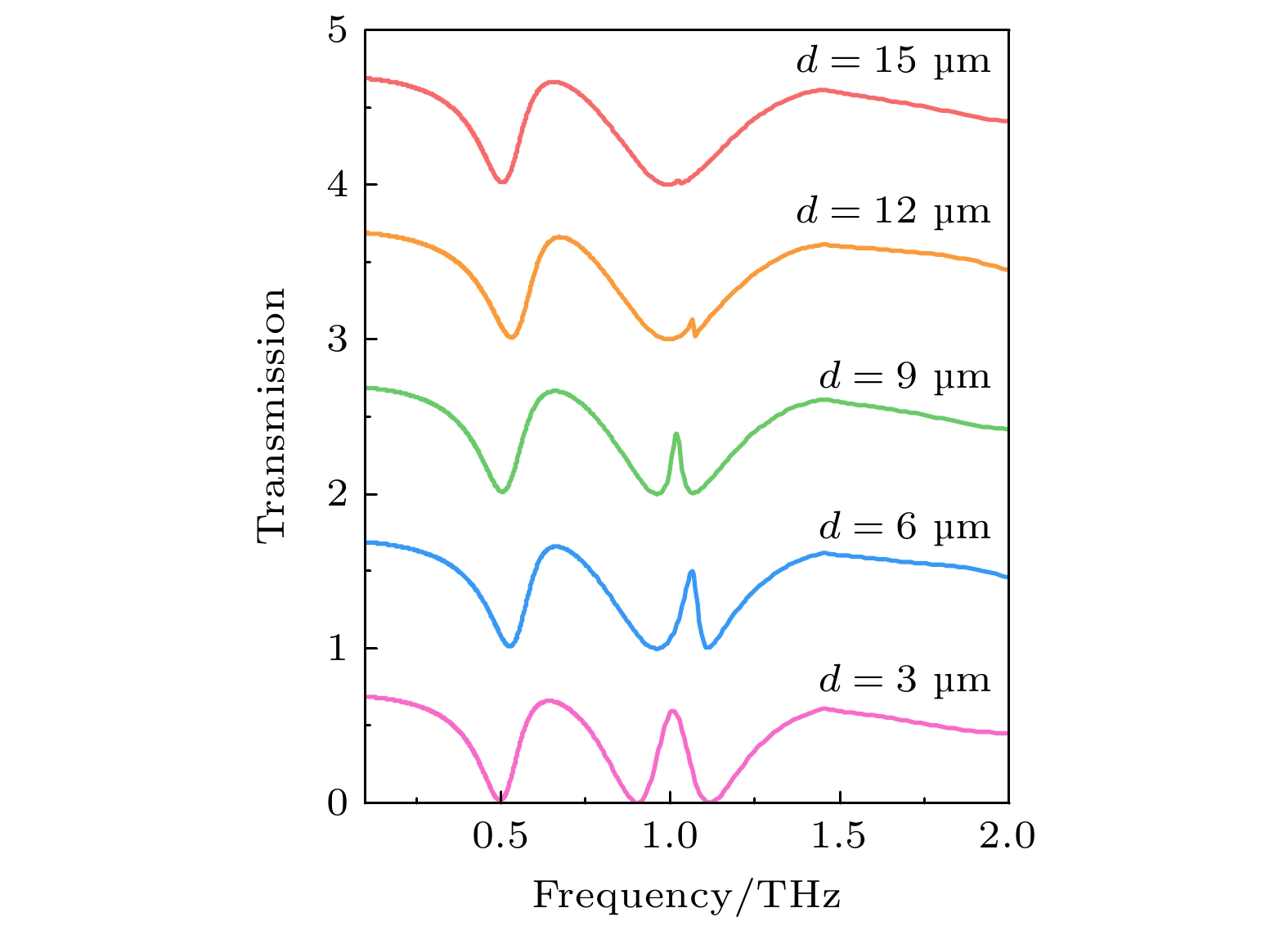
图 8 阵列结构透射率随着间距d增大变化情况
Figure 8. The variation of transmission in the array structure with increasing spacing d.
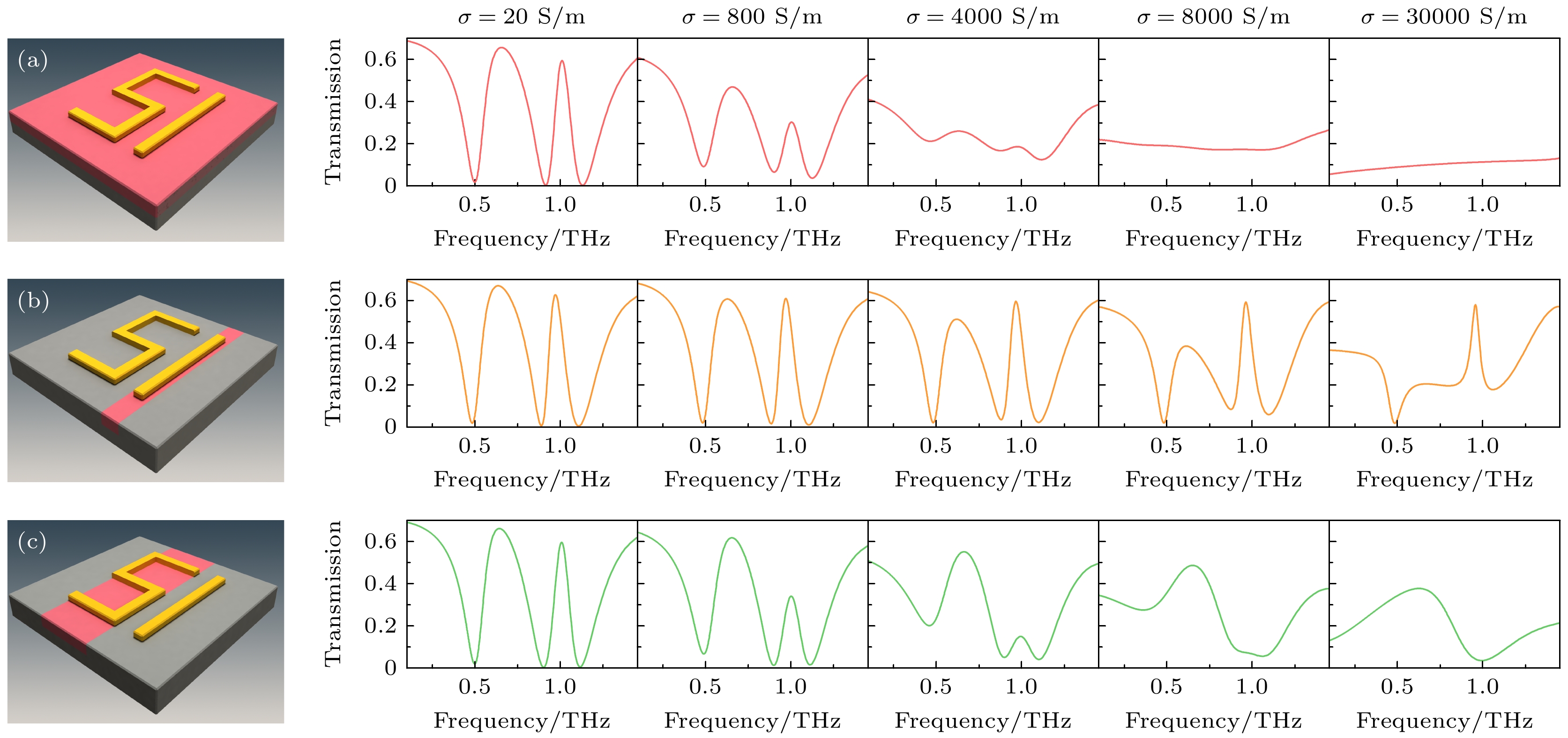
图 9 当VO2电导率σ从20 S/m增加到30000 S/m时, 三种典型结构的透射光谱变化情况: (a) VO2完全覆盖基底表面; (b) VO2位于金纳米条下方; (c) VO2位于S型金开口环下方
Figure 9. Evolution of transmission spectra for three characteristic structures as the electrical conductivity σ of VO2 increases from 20 S/m to 30, 000 S/m: (a) VO2 fully covering the substrate surface; (b) VO2 located beneath the gold nanorod; (c) VO2 positioned under the S-shaped split-ring.
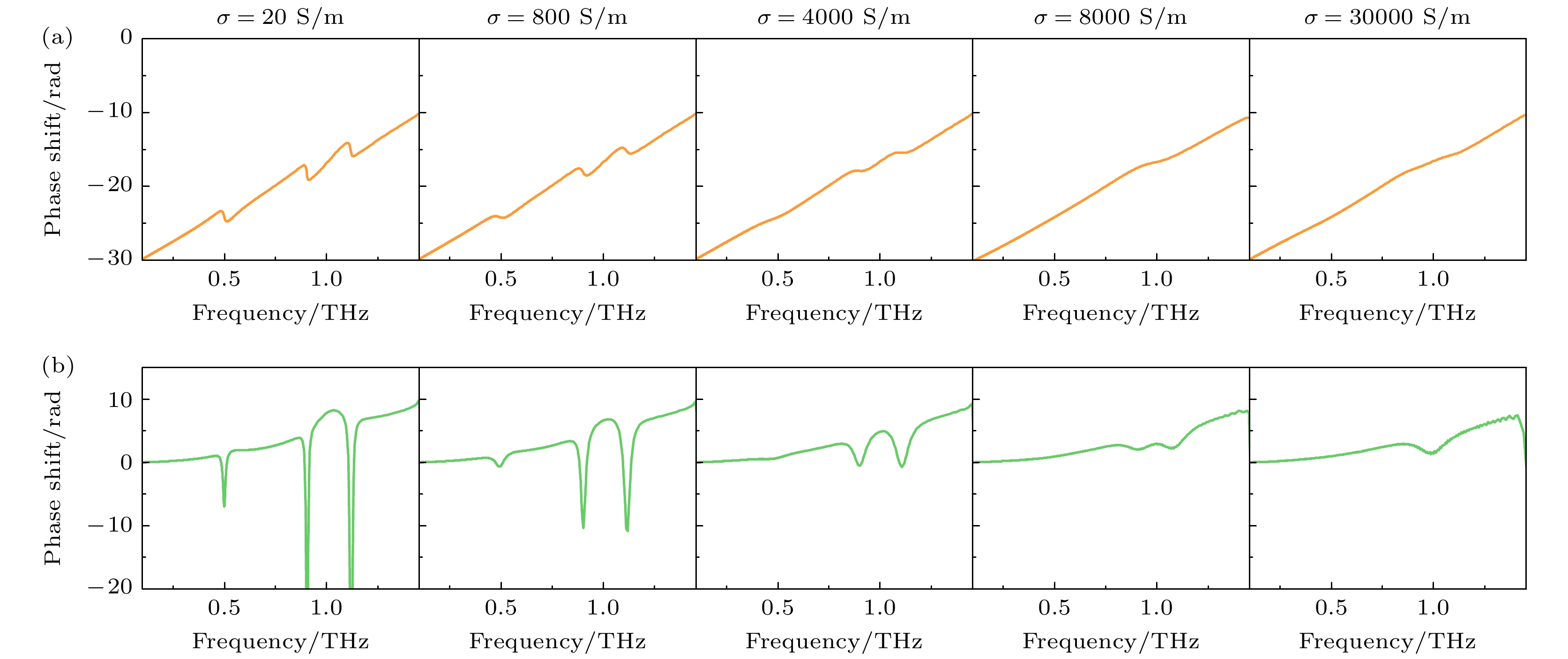
图 10 当VO2电导率σ从20 S/m增加到30000 S/m时, 阵列结构的(a) 相位与(b) 群延时变化情况
Figure 10. As the conductivity σ of VO2 rises from 20 S/m to 30000 S/m, the array structure exhibits changes in (a) phase and (b) group delay.
表 1 多极矩及其远场散射功率表达式
Table 1. Multipole moment and its expression for far-field scattering power.
多极子 矩表达式 散射功率 电偶极子 (ED) $ p = \dfrac{1}{i\omega} \displaystyle\int J({\bf{r}}) d^3{\bf{r}} $ $ I_p = \dfrac{2\omega^4}{3 c^3} |{\bf{p}}|^2 $ 磁偶极子 (MD) $ m = \dfrac{1}{ic} \displaystyle\int {\bf{r}} \times J({\bf{r}}) d^3{\bf{r}} $ $ I_m = \dfrac{2\omega^4}{3 c^3} |{\bf{m}}|^2 $ 环偶极子 (TD) $ T = \dfrac{1}{10 c} \displaystyle\int \{ [{\bf{r}} \cdot J({\bf{r}})]{\bf{r}} - 2[{\bf{r}} \cdot {\bf{r}}]J({\bf{r}}) \} d^3{\bf{r}} $ $ I_T = \dfrac{2\omega^6}{3 c^5} |{\bf{T}}|^2 $ 电四偶极子 (EQ) $ Q_{\alpha\beta} = \dfrac{1}{2 i\omega} \displaystyle\int \{ r_{\alpha}J_{\beta}({\bf{r}}) + r_{\beta}J_{\alpha}({\bf{r}}) - \dfrac{2}{3}[{\bf{r}} \cdot J({\bf{r}})]\delta_{\alpha\beta} \} d^3{\bf{r}} $ $ I^e_Q = \dfrac{\omega^6}{5 c^5} \displaystyle\sum|Q_{\alpha\beta}|^2 $ 磁四偶极子 (MQ) $ M_{\alpha\beta} = \dfrac{1}{3 c} \displaystyle\int \{ [{\bf{r}} \times J({\bf{r}})]_{\alpha}r_{\beta} + [{\bf{r}} \times J({\bf{r}})]_{\beta}r_{\alpha} \} d^3{\bf{r}} $ $ I^m_Q = \dfrac{\omega^6}{20 c^5} \displaystyle\sum|M_{\alpha\beta}|^2 $  DownLoad: CSV
表 2 类电磁诱导透明超表面的群延时性能与本研究的对比
Table 2. Comparison of group delay performance EIT-like metasurfaces with that of this study.
DownLoad: CSV
-
[1] Pendry J B 2000 Phys. Rev. Lett. 85 18
 Google Scholar
[2] Seeds A J, Shams H, Fice M J, Renaud C C 2014 J Lightwave Technol. 33 519
[3] Jepsen P U, Cooke D G, Koch M 2011 Laser Photonics Rev. 5 124
Google Scholar
[4] Schurig D, Mock J J, Justice B J, Cummer S A, Pendry J B, Starr A F, Smith D R 2006 Science 314 977
Google Scholar
[5] Zhang S, Genov D A, Wang Y, Liu M, Zhang X 2008 Phys. Rev. Lett. 101 047401
Google Scholar
[6] Hu X G, Yuan S, Armghan A, Liu Y, Jiao Z, Lv H J, Zeng C, Huang Y, Huang Q Z, Wang Y, Xia J S 2017 J. Phys. D: Appl. Phys. 50 1361
[7] Wang S, Zhang M, Ju A A, Wang B, Zhao R, Kong Z B, Wang K S, Lian P F 2023 Opt. Mater. 13 12
[8] Wang Z F, Wu J, Hou J Q, Wan F Y, Fu J H, Wu Q, Ran L X, Denidni T A 2025 Appl. Phys. Lett. 126 211701
Google Scholar
[9] Yahiaoui R, Burrow J A, Mekonen S M, Sarangan A, Mathews J, Agha I, Searles T A 2018 Phys. Rev. B 97 155403
Google Scholar
[10] Yu W, Meng H Y, Chen Z J, Li X P, Zhang X, Wang F Q, Wei Z C, Tan C H, Huang X G, Li S T 2018 Opt. Commun. 414 29
Google Scholar
[11] Jia Z P, Huang L, Su J B, Tang B 2020 Appl. Phys. Express 13 072006
Google Scholar
[12] Zhang Y T, Liu S Y, Huang W, Dong E X, Li H Y, Shi X T, Liu M, Zhang W T, Yin S, Luo Z Y 2022 Chinese Phys. B 31 068702
Google Scholar
[13] Nourinovin S, Rahman M M, Naftaly M, Philpott M P, Abbasi Q H, Alomainy A 2024 IEEE Trans. Biomed. Eng. 71 2180
Google Scholar
[14] Wang H, Zhang D Q, Jin Z W, Fang B, Pan G M, Hong Z, Shu F Z 2025 Phys. Scr. 100 035505
Google Scholar
[15] Zhou M, Li Y C, Tian J P, Yang R C 2025 Phys. Lett. A 536 130300
Google Scholar
[16] Shu C, Mei J S, Sun H Y, Chen L y, Sun Y 2024 Opt. Quant. Electron. 56 43
Google Scholar
[17] Huang W, Cao S T, Liang S J, Shan Y, Zhang W T 2025 Phys. Rev. B 111 045429
Google Scholar
[18] Le-Van Q, Zoethout E, Geluk E J, Ramezani M, Berghuis M, Gómez Rivas J 2019 Adv. Opt. Mater. 7 1801451
Google Scholar
[19] Manjappa M, Srivastava Y K, Singh R 2016 Phys. Rev. B 94 161103
Google Scholar
[20] Khlopin D, Laux F, Wardley W P, Martin J, Wurtz G A, Plain J, Bonod N, Zayats A V, Dickson W, Gérard D 2017 J. Opt. Soc. Amer. B 34 691
Google Scholar
[21] Tan T C W, Srivastava Y K, Manjappa M, Plum E, Singh R 2018 Appl. Phys. Lett. 112 201111
Google Scholar
[22] Burrow J A, Yahiaoui R, Sarangan A, Mathews J, Agha I, Searles T A 2019 Opt. Lett. 44 2705
Google Scholar
[23] Karmakar S, Kumar D, Varshney R K, Roy Chowdhury D 2020 Opt. Lett. 45 3386
Google Scholar
[24] Seliuta D, Šlekas G, Valušis G, Kancleris ff 2019 Opt. Lett. 44 759
Google Scholar
[25] Tan T C W, Plum E, Singh R 2020 Adv. Optical Mater. 20 1901572
[26] Luo C C, Tan T C W, Fan Z Y, Chen L, Singh R, Zhu Y M, Zhuang S L 2024 Sensor Actuat. B. 410 135628
Google Scholar
[27] Michaeli L, Suchowski H, Ellenbogen T 2020 Laser Photonics Rev. 14 1900204
Google Scholar
[28] Ning R X, Li D K, Yang T L, Chen Z H, Qian H W 2019 Sci. Rep. 9 15801
Google Scholar
[29] Luo H, Luo J, Chu H C, Ji W J, Lai Y 2025 Phys. Rev. Applied 23 024025
Google Scholar
[30] Li T F, Chu Z T, Yang J, Ding C, Jia Y X, Fu X M, Zhao S, Liu Z T, Feng C Q, Wang J F 2025 Mater. Today Nano 29 100559
Google Scholar
[31] Mei J S, Song C L, Shu C 2021 Opt. Commun. 488 126851
Google Scholar
[32] Wang J P, Fan C Z 2025 Phys. Scr. 100 025517
Google Scholar
[33] 胡树南, 李德琼, 詹杰, 高恩多, 王琦, 刘南柳, 聂国政 2025 物理学报 74 097801
Google Scholar
Hu S N, Li D Q, Zhan J, Gao E D, Wang Q, Liu N L, Nie G Z 2025 Acta Phys. Sin. 74 097801
Google Scholar
[34] Guo W P, Wang Y, Liu C X, Tan P, Wang L Guan Chao Li, Tian H 2024 Appl. Phys. Lett. 125 241703
Google Scholar
[35] Chen M M, Yang X X, Shu F Z 2024 Mater. Res. Bull. 180 113000
Google Scholar
[36] Wang Z, Xie J, Fan C Z 2024 J. Phys. D: Appl. Phys. 57 395107
Google Scholar
[37] Liu N, Langguth L, Weiss T, Kästel J, Fleischhauer M, Pfau T, Giessen H 2009 Nat. Mater. 8 758
Google Scholar
[38] Liu H, Fan Y X, Chen H G, Li L, Tao Z Y 2019 Opt. Commun. 445 277
Google Scholar
[39] Li C, Zhu W, Liu Z, Pan R H, Hu S, Du S, Li J J, Gu C Z 2020 Nanoscal 12 10065
Google Scholar
[40] Zhao Y C, Zhang Y X, Shi Q W, Liang S X, Huang W X, Kou W, Yang Z Q 2018 ACS Photonics 5 3040
Google Scholar
[41] Miroshnichenko A E, Flach S, Kivshar Y S 2010 Rev. Mod. Phys. 82 2257
Google Scholar
[42] Fan J X, Li Z L, Xue Z Q, Xing H Y, Lu D, Xu G Z, Gu J Q, Han J G, Cong L Q 2023 Opto-Electron. Sci. 2 230006
Google Scholar
[43] Fan F, Hou Y, Jiang Z W, Wang X H, Chang S J 2012 Appl. Opt. 51 4589
Google Scholar
[44] Gao W K, Chen F, Yang W X 2025 Opt. Commun. 590 132027
Google Scholar
[45] Liang D H, Chen T 2023 Diam. Relat. Mater. 131 109613
Google Scholar
[46] Lu J J, Li H, Qiu X J, Long H, Shen J 2025 Photonics Nanostruct. Fundam. Appl. 64 101370
Google Scholar
[47] Xu H Y, Xu H, Yang X J, Li M, Yu H F, Cheng Y X, Zhan S P, Chen Z Q 2024 Phys. Lett. A 504 129401
Google Scholar
[48] Zhang Z J, Yang J B, Han Y X, He X, Zhang J J, Huang J, Chen D B, Xu S Y, Xie W L 2020 Appl. Phys. A 126 199
Google Scholar

 DownLoad:
Metrics
- Abstract views: 15
- PDF Downloads: 0
- Cited By: 0
