


Accepted Papers
Recent catalogue
-
Vol.74 No.24
2025-12-20
-
Vol.74 No.23
2025-12-05
-
Vol.74 No.22
2025-11-20
-
Vol.74 No.21
2025-11-05
- All Archive
SPECIAL TOPIC—Instrumentation and metrology for ultrafast atomic and molecular spectroscopy
2025, 74 (24): 240101.
doi: 10.7498/aps.74.240101
Abstract +

SPECIAL TOPIC—Atomic, molecular and materials properties data
2025, 74 (24): 240102.
doi: 10.7498/aps.74.240102
Abstract +

GENERAL
2025, 74 (24): 240201.
doi: 10.7498/aps.74.20251073
Abstract +
Owing to, Solid-state batteries have gradually become the focus of people’s attention and research in recent years due to the advantages of high energy density and high safety factor. Lithium dendrites are a key factor affecting battery safety and service life, and in severe cases, battery short circuits can occur. Compared with liquid batteries, solid-state batteries rely on solid-state electrolytes with higher mechanical strength, which can effectively inhibit the growth of lithium dendrites, but with the increase of the number of charge-discharge cycles, the dead lithium produced by the incomplete dissolution of lithium dendrites gradually accumulates, and the performance of the battery gradually decreases. In this work, the problem of dead lithium in solid-state batteries is studied by using COMSOL Multiphysics 6.2 finite element simulation software. Due to the fact that existing research on dead lithium mainly focuses on phase field models combined with binary physics, there is little research on the influence of electrochemical parameters on dead lithium. Therefore, the phase field method is used to simulate the dissolution of lithium dendrites and the formation of dead lithium under the coupling of force-thermal-electrochemical fields. When the heat transfer model is coupled, the difference in the morphology of dead lithium before and after the coupled heat transfer model is further studied by applying an external pressure to change the stress of lithium dendrites. When the coupled mechanical field changes, the morphology of dead lithium before and after the coupled mechanical field is further studied by changing the temperature magnitude. At the same time, the effects of changes in three electrochemical parameters, namely diffusion coefficient, interfacial mobility and anisotropic strength, on the area of dead lithium are also explored. The research results indicate that when the heat transfer model or mechanical field is coupled into the phase field model, the dendrite dissolution cut-off time and dead lithium area will change. When the base rises at high temperature or when low external pressure or high external pressure is applied, the area of dead lithium decreases. For changing the electrochemical parameters, reducing the diffusion coefficient, increasing the interfacial mobility and reducing the anisotropic strength can effectively reduce the area of dead lithium.
SPECIAL TOPIC—Principles and applications of quantum optics·COVER ARTICLE
2025, 74 (24): 240301.
doi: 10.7498/aps.74.20251454
Abstract +
GENERAL
2025, 74 (24): 240501.
doi: 10.7498/aps.74.20251142
Abstract +
GENERAL
2025, 74 (24): 240502.
doi: 10.7498/aps.74.20251102
Abstract +
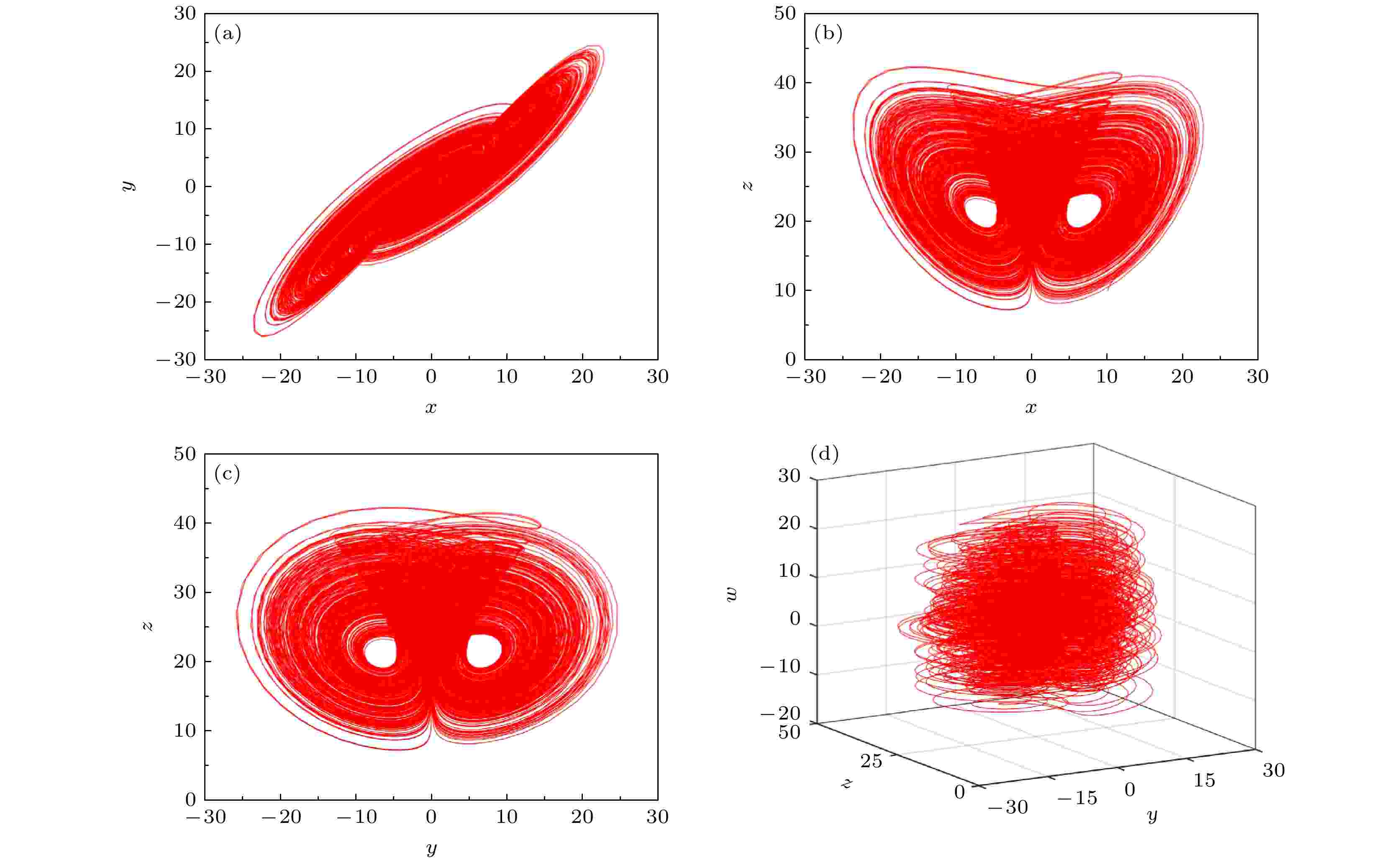
Memristors exhibit controllable nonlinear characteristics, generating chaotic signals that are characterized by randomness, sensitivity, and unpredictability, thereby demonstrating significant potential applications in information encryption and signal processing. With the integration of chaos theory and electronic technology, constructing memristive hyperchaotic systems has become a hot topic in nonlinear science and information security. To overcome the limitation of monotonic dynamic characteristics in traditional chaotic systems, we design a novel memristor-based hyperchaotic system with richer dynamic behavior and higher application value in this paper. Moreover, the characteristic analysis, theoretical verification, application exploration, and hardware implementation are conducted to support the engineering applications of the system. Building upon the classical Chen system, this work is innovatively combined with a cubic nonlinear magnetically controlled memristor model as a feedback element. By establishing a mathematical model of the memristor and coupling it with the state equations of the Chen system, we design a four-dimensional memristor-based hyperchaotic system. First, by integrating numerical computation with differential equation theory, a comprehensive mathematical model is established to analyze fundamental properties, such as symmetry and dissipativity, thereby validating the system’s rationality. Second, the system’s dynamical behaviors are analyzed, including attractor phase diagrams, Lyapunov exponents, power spectra, parameter effects, transient dynamics, and coexisting attractors. Simultaneously, variational methods are utilized to analyze unstable periodic orbits within the system. A symbolic coding approach based on orbital characteristics is established to convert orbital information into symbolic sequences, and orbital pruning rules are explored to provide a basis for optimal orbital control. Furthermore, a digital image encryption method is proposed based on this system. Using chaotic sequences as keys, image pixels are scrambled and diffused. The effectiveness of encryption is validated through histogram analysis, correlation analysis, information entropy evaluation, and testing of anti-attack capabilities. Finally, a DSP-based digital circuit hardware platform is constructed to run the system, and the hardware experimental results are compared with software simulation outcomes. These findings reveal that the introduction of memristors induces linearly distributed equilibrium points in phase space, generating hidden attractors that enrich the chaotic behavior of the system. The simulation of dynamic behavior confirms the rich dynamics of this four-dimensional memristor-based hyperchaotic system. The proposed digital image encryption method demonstrates robust security performance. The DSP hardware experiments and software simulations yield highly consistent attractor phase diagrams, validating the correctness and feasibility of the system.
SPECIAL TOPIC—AI + Physical Science
2025, 74 (24): 240701.
doi: 10.7498/aps.74.20250989
Abstract +
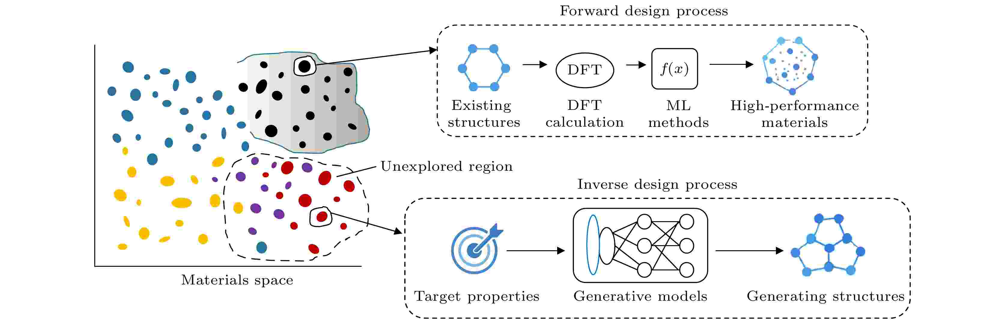
In recent years, the application of machine learning in materials science has significantly accelerated the discovery of new materials. In particular, when combined with traditional methods such as first-principles calculations, machine learning models have proven effective in screening potential high-performance materials from existing databases. However, these methods are largely limited by the known chemical spaces, making it difficult to achieve the active design of novel material structures. To overcome this limitation, generative models have become a promising tool for inverse material design, providing new avenues for exploring unknown structures and property spaces. Although existing generative models have achieved initial progress in crystal structure generation, achieving property-guided material generation remains a significant challenge. In this review paper, we first introduce the representative generative models recently applied to materials generation, including CDVAE, MatGAN, and MatterGen, and analyzes their basic abilities and limitations in structural generation. We then focus on strategies for incorporating target properties into generative models to generate the property-guided structure. Specifically, we discuss four representative methods: Con-CDVAE based on target property vectors, SCIGEN with integrated structural constraints and guidance mechanisms, a fine-tuned version of MatterGen leveraging adapter-based property control, and a CDVAE latent space optimization strategy guided by property objectives. Finally, we summarize the key challenges faced by property-guided generative models and provide an outlook on future research directions. This review aims to offer researchers a systematic reference and inspiration for advancing property-driven generative approaches in material design and provides researchers with a systematic reference and insight into the advancement of property-driven generative methods for materials design.
GENERAL
2025, 74 (24): 240702.
doi: 10.7498/aps.74.20251146
Abstract +

THE PHYSICS OF ELEMENTARY PARTICLES AND FIELDS
2025, 74 (24): 241301.
doi: 10.7498/aps.74.20250639
Abstract +
An unresolved issue in the study of baryon non-leptonic decays is that the theoretical values describing the s- and p-wave amplitudes of such decays cannot simultaneously accord well with experimental values. Compared with previous literature, this paper adopts the covariant chiral effective theory framework and calculates the one-loop corrections to the s- and p-wave amplitudes by using the extended minimal subtraction (EMS) scheme, and also takes into account the contributions from intermediate pion states that are neglected in previous studies (the contributions from intermediate decuplet states are not considered here). Unlike infrared regularization and the extended on-shell subtraction scheme, EMS is easier to implement and also avoids over-subtraction. Apart from the typical chiral logarithmic term mslnms obtained in heavy-baryon formalism, the covariant calculation retains many non-local contributions that are not negligible. These non-local contributions vary with loop diagrams and intermediate states, making the complete covariant results significantly different from those from the simple chiral logarithmic structures in heavy-baryon formalism, which may alleviate the tension between the s- and p-wave components of the decay amplitudes. Subsequent numerical analysis confirms this conjecture. Two approaches are adopted to obtain covariant theoretical predictions: s-wave fitting and p-wave fitting. According to the fitted predictions and chi-squares of fitness, the s-wave fitting yields s-wave predictions slightly inferior to those under heavy-baryon formalism, but the resulting p-wave predictions are considerably improved compared with the heavy-baryon formalism predictions. The p-wave fitting produces p-wave predictions closer to experimental values, while the heavy-baryon predictions differ significantly from the experimental values. The resulting s-wave predictions from p-wave fitting show noticeable discrepancies with experimental data, but the heavy-baryon predictions are even worse. Therefore, working in the covariant framework, the tension between s- and p-wave amplitudes for baryon non-leptonic decays is significantly alleviated in comparison with that in heavy-baryon formalism. In addition, it is found that the contributions from intermediate pion states may be neglected in many cases, but are important and must be kept for decays with smaller experimental values.
SPECIAL TOPIC—Semiconductor physics and devices
2025, 74 (24): 241302.
doi: 10.7498/aps.74.20251120
Abstract +
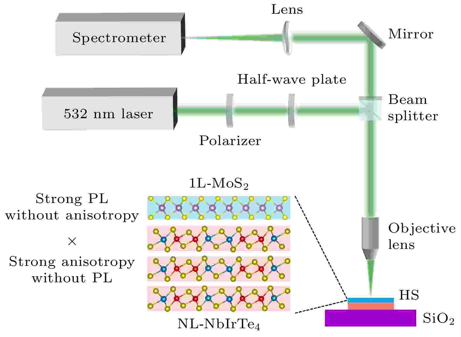
Luminescence and anisotropy in two-dimensional (2D) materials have important implications for both fundamental material physics and potential applications such as polarized light-emitting devices. However, many natural-occuring 2D materials typically exhibit either luminescence or anisotropy, but not both. In this work, we utilize van der Waals (vdW) engineering to construct a heterostructure (HS) with anisotropic luminescent properties, which is composed of isotropic monolayer (1L) MoS2 (with strong intrinsic luminescence) and low-symmetry NbIrTe4 (strong anisotropy without photoluminescence). Experimentally, we characterize the optical response of the HS by using angle-resolved PL spectroscopy. The results indicate that the intrinsic anisotropic potential field of NbIrTe4 at the interface effectively breaks the in-plane isotropic symmetry of MoS2, inducing a pronounced polarization-dependent emission of A and B excitons. The anisotropy ratio is enhanced to ~1.58, corresponding to a linear polarization degree of approximately 22%. This work provides new insights into 2D interfacial coupling and offers useful guidance for the design and engineering of next-generation high-performance, tunable polarized light-emitting devices.

- 1
- 2
- 3
- 4
- 5
- ...
- 11
- 12


