


-
透明导电氧化物 (transparent conductive oxides, TCOs)薄膜和透明氧化物半导体 (transparent oxide semiconductors, TOSs) 薄膜具有高透明度和良好的导电率等特点, 广泛应用于太阳能电池、平板显示、智能窗以及透明柔性电子器件等领域. 大多数TCOs和TSOs薄膜主要是以氧化铟、氧化锌和氧化锡三种材料为基础衍生来的, 其中, 氧化铟薄膜中In元素有毒、含量稀少且价格昂贵, 会造成环境污染; 氧化锌薄膜对酸或碱刻蚀液敏感, 薄膜图形化困难; 氧化锡薄膜不仅无毒、无污染、价格低廉, 还具有良好的电学性能和化学稳定性, 具有巨大的发展潜力. 目前, 薄膜的制备主要依赖于真空镀膜技术. 此类技术的缺点在于设备结构复杂且价格昂贵、能耗高、工艺复杂、生产成本高等. 相比传统真空镀膜技术, 溶胶-凝胶法具有工艺简单、成本低等优点, 受到了人们的广泛关注. 本文从TCOs和TSOs薄膜的发展现状和发展趋势出发, 先介绍了氧化锡薄膜的结构特性、导电机制、元素掺杂理论以及载流子散射机理, 然后介绍了溶胶-凝胶法原理和制备方法, 接着介绍了近些年来溶胶-凝胶法制备氧化锡基薄膜在n型透明导电薄膜、薄膜晶体管以及p型半导体薄膜中的应用和发展, 最后总结了当前存在的问题以及今后研究的方向.Transparent conductive oxide (TCO) films and transparent oxide semiconductor (TOS) films have been widely adopted in solar cells, flat panel displays, smart windows, and transparent flexible electronic devices due to their advantages of high transparency and good conductivity and so on. Most of TCO and TOS films are mainly derived from indium oxide, zinc oxide and tin oxide. Among these materials, the In element is toxic, rare and expensive for indium oxide film, which will cause environmental pollution; zinc oxide film is sensitive to acid or alkali etchants, resulting in a poor formation of film patterning; tin oxide film is not only non-toxic, eco-friendly, and cheap but also has good electrical properties and strong chemical stability. Thus, tin oxide has a great potential for developing the TCO and TOS films. At present, the film is prepared mainly by the vacuum deposition technique. The drawbacks of this technique are complex and expensive equipment system, high energy consumption, complicated process and high-cost production. However, compared with the vacuum deposition technique, the sol-gel method has attracted extensive attention because of its virtues such as simple process and low cost. In this paper, we review the development status and trend of TCO and TOS films. First, the structural characteristics, conductive mechanism, element doping theory and carrier scattering mechanism of tin oxide thin films are introduced. Then the principle of sol-gel method and correlative film fabrication techniques are illustrated. Subsequently, the application and development of tin oxide-based thin films prepared by sol-gel method in n-type transparent conductive films, thin-film transistors and p-type semiconductor films in recent years are described. Finally, current problems and future research directions are also pointed out.
-
Keywords:
- tin oxide /
- sol-gel method /
- transparent conductive oxide films /
- transparent semiconductor oxide films /
- thin film transistor /
- p-type semiconductor films
[1] Grundmann M, Frenzel H, Lajn A, Lorenz M, Schein F, von Wenckstern H 2010 Phys. Status Solidi Appl. Mater. Sci. 207 1437
 Google Scholar
[2] Yu X, Marks T J, Facchetti A 2016 Nat. Mater. 15 383
Google Scholar
[3] Park J, Kim H, Kim I 2014 J. Electroceram. 32 117
Google Scholar
[4] Hosono H 2007 Thin Solid Films 515 6000
Google Scholar
[5] Park J S, Maeng W J, Kim H S, Park J S 2012 Thin Solid Films 520 1679
Google Scholar
[6] Facchetti A, Marks T J 2010 Transparent Electron. From Synth. to Appl. 561 2002
[7] Fortunato E, Barquinha P, Martins R 2012 Adv. Mater. 24 2945
Google Scholar
[8] Chopra K L, Major S, Pandya D K 1983 Thin Solid Films. 102 1
Google Scholar
[9] Nomura K, Ohta H, Takagi A, Kamiya T, Hirano M, Hosono H 2004 Nature 432 488
Google Scholar
[10] Yang T, Qin X, Wang H H, Jia Q, Yu R, Wang B, Wang J, Ibrahim K, Jiang X, He Q 2010 Thin Solid Films 518 5542
Google Scholar
[11] Fang F, Zhang Y, Wu X, ShaO Q, Xie Z 2015 Mater. Res. Bull. 68 240
Google Scholar
[12] Ning H L, Liu X Z, Zhang H K, Fang Z Q, Cai W, Chen J Q, Yao R H, Xu M, Wang L, Lan L F, Peng J B, Wang X F, Zhang Z C 2017 Materials (Basel) 10 24
Google Scholar
[13] Jadhav H, Suryawanshi S, More M A, Sinha S 2017 Appl. Surf. Sci. 419 764
Google Scholar
[14] El-Gendy Y A 2017 Phys. B Condens. Matter 526 59
Google Scholar
[15] Bae J Y, Park J, Kim H Y, Kim H S, Park J S 2015 ACS Appl. Mater. Interfaces 7 12074
Google Scholar
[16] Jiménez V M, Espinós J P, González-Elipe A R, Caballero A, Yubero F 1999 J. Phys. IV 9 749
Google Scholar
[17] Choi Y J, Gong S C, Johnson D C, Golledge S, Yeom G Y, Park H H 2013 Appl. Surf. Sci. 269 92
Google Scholar
[18] Park J W, Kang B H, Kim H J 2020 Adv. Funct. Mater. 30 1904632
Google Scholar
[19] Ning H L, Liu X Z, Ruan H G, Peng C, Huang F X, Deng Y X, Yuan W J, Yao R H, Qiu B, Wang X F, Peng J B 2019 AIP Adv. 9 11
Google Scholar
[20] Salmani E, Laghrissi A, Lamouri R, Rouchdi M, Dehmani M, Ez-Zahraouy H, Hassanain N, Mzerd A, Benyoussef A 2018 Opt. Quantum Electron. 50 85
Google Scholar
[21] Pons D, Bourgoin J C 1985 J. Phys. C Solid State Phys. 18 3839
Google Scholar
[22] Shukla T S 2012 J. Sens. Technol. 2 102
Google Scholar
[23] Scanlon D O, Watson G W 2012 J. Mater. Chem. 22 25236
Google Scholar
[24] Terrier C, Chatelon J P, Berjoan R, Roger J A 1995 Thin Solid Films 263 37
Google Scholar
[25] Mäki-Jaskari M A, Rantala T T 2002 Phys. Rev. B - Condens. Matter Mater. Phys. 65 1
Google Scholar
[26] Kılıç Ç, Zunger A 2002 Phys. Rev. Lett. 88 955011
Google Scholar
[27] Singh A K, Janotti A, Scheffler M, van De Walle C G 2008 Phys. Rev. Lett. 101 1
Google Scholar
[28] 倪佳苗, 赵修建, 郑小林, 赵江 2009 真空科学与技术学报 29 531
Google Scholar
NI J M, Zhao X J, Zheng X L, Zhao J 2009 Zhenkong Kexue Yu Jishu Xuebao 29 531
Google Scholar
[29] 望咏林, 颜悦, 沈玫, 贺会权, 张官理 2006 材料导报 20 317
Google Scholar
Wang Y L, Yan Y, Shen M, He H Q, Zhang G L 2006 Mater. Rev. 20 317
Google Scholar
[30] 刘宏燕, 颜悦, 望咏林, 伍建华, 张官理, 厉蕾 2015 航空材料学报 35 63
Liu H Y, Yan Y, Wang Y L, Wu J H, Zhang G L, Li L J. Aeronaut. Mater. 35 63 (in Chinese)
[31] 王立坤, 郁建元, 王丽, 牛孝友, 付晨, 邱茹蒙, 晏伟静, 赵洪力 2018 硅酸盐学报 46 590
Wang L K, Yu J Y, Wang L, Niu X Y, Fu C, Qiu Y M, Yan W J, Zhao H L 2018 J. Chin. Ceram. Soc. 46 590
[32] Noguchi S, Sakata H 1980 J. Phys. D. Appl. Phys. 13 1129
Google Scholar
[33] Galceran Mestres M, Pujol Baiges M C, Aguiló Díaz M 2010 Ph. D. Dissertation (Tarragona: Universitat Rovira i Virgili.)
[34] 武志刚, 高建峰 2010 精细化工 027 21
Wu Z G, Gao J F 2010 Fine Chem. 027 21
[35] Park B, Na S Y, Bae I G 2019 Sci. Rep. 9 1
Google Scholar
[36] Filipovic L, Selberherr S, Mutinati G C, Brunet E, Steinhauer S, Köck A, Teva J, Kraft J, Siegert J, Schrank F 2013 Proc. world. Cong. Eng. 2 987
[37] Aymerich M, Gómez-Varela A I, Álvarez E, Flores-Arias M T 2016 Materials (Basel. 9 728
Google Scholar
[38] Lau G K, Shrestha M 2017 Micromachines 8 1
Google Scholar
[39] Krebs F C 2009 Sol. Energy Mater. Sol. Cells. 93 394
Google Scholar
[40] 李宁, 卢迪芬 2004 玻璃与搪瓷 6 12
Google Scholar
Li N, Lu D F 2004 Glass&Enamel 6 12
Google Scholar
[41] Korotcenkov G, Brinzari V, Schwank J, DiBattista M, Vasiliev A 2001 Sensors Actuators, B Chem. 77 244
Google Scholar
[42] Falcony C, Aguilar-Frutis M A, García-Hipólito M 2018 Micromachines 9 1
Google Scholar
[43] Landau L, Levich B 1988 Dyn. Curved Front. 17 141
[44] Vilà A, Gomez A, Portilla L, Morante J R 2014 Thin Solid Films 553 118
Google Scholar
[45] Betz U, Kharrazi Olsson M, Marthy J, Escolá M F, Atamny F 2006 Surf. Coatings Technol. 200 5751
Google Scholar
[46] Lee S M, Lee J M, Kwon S J, Cho E S 2013 Mol. Cryst. Liq. Cryst. 586 138
Google Scholar
[47] May C, Tomita Y, Toerker M, Eritt M, Loeffler F, Amelung J, Leo K 2008 Thin Solid Films 516 4609
Google Scholar
[48] Park S K, Han J I, Kim W K, Kwak M G 2001 Thin Solid Films 397 49
Google Scholar
[49] Agashe C, Major S S 1996 J. Phys. D. Appl. Phys. 29 2988
Google Scholar
[50] Luo Y R 2007 Comprehensive Handbook of Chemical Bond Energies(Boca Raton: CRC Press) p1
[51] Karthick P, Vijayanarayanan D, Sridharan M, Ananth A K, Sanjeeviraja C, Jeyadheepan K 2017 Thin Solid Films 631 1
Google Scholar
[52] Tran Q P, Fang J S, Chin T S 2015 Mater. Sci. Semicond. Process. 40 664
Google Scholar
[53] Lee K M, Shih K L, Chiang C H, Suryanarayanan V, Wu C G 2014 Thin Solid Films 570 7
Google Scholar
[54] Upadhyay J P, Vishwakarma S R, Prasad H C 1988 Thin Solid Films 167 7
Google Scholar
[55] An H R, Kim C, Oh S T, Ahn H J 2014 Ceram. Int. 40 385
Google Scholar
[56] Elangovan E, Shivashankar S A, Ramamurthi K 2005 J. Cryst. Growth 276 215
Google Scholar
[57] Turgut G 2015 Thin Solid Films 594 56
Google Scholar
[58] Turgut G, Keskenler E F, Aydin S, Sönmez E, Doǧan S, Düzgün B, Ertuǧrul M 2013 Superlattices Microstruct. 56 107
Google Scholar
[59] Turgut G 2015 Philos. Mag. 95 1607
Google Scholar
[60] Huang Y, Li D, Feng J, Li G, Zhang Q 2010 J. Sol-Gel Sci. Technol. 54 276
Google Scholar
[61] Gokulakrishnan V, Parthiban S, Jeganathan K, Ramamurthi K 2011 J. Mater. Sci. 46 5553
Google Scholar
[62] Marius G, Heiko F, Alexander L, Michael L, Friedrich S, H. von W 2010 Phys. Status Solidi A 1449 1437
[63] Jang B, Kim T, Lee S, Lee W Y, Kang H, Cho C S, Jang J 2018 IEEE Electron Device Lett. 39 1179
Google Scholar
[64] Avis C, Ki Y G, Jang J, 2019 Materials (Basel) 12 3341
Google Scholar
[65] Liu C, Wang Z 2018 AM-FPD 2018 - 25 th International Workshop on Active-Matrix Flatpanel Displays Devices Kyoto, Japan July 3−6, 2018 p
[66] Lee W, Jang B, Lee S, Kim T, Jang J 2018 25 th Int. Work. Act. Flatpanel Displays Devices 1
[67] Jang J, Kitsomboonloha R, Swisher S L, Park E S, Kang H, Subramanian V 2013 Adv. Mater. 25 1042
Google Scholar
[68] Huang G, Duan L, Dong G, Zhang D, Qiu Y 2014 ACS Appl. Mater. Interfaces 6 20786
Google Scholar
[69] Zhao Y, Dong G, Duan L, Qiao J, Zhang D, Wang L, Qiu Y 2012 RSC Adv. 2 5307
Google Scholar
[70] Kim S J, Yoon S, Kim H J 2014 Japanese journal of applied physics 2 1
Google Scholar
[71] Liu A, Zhu H, Sun H, Xu Y, Noh Y Y 2018 Adv. Mater. 30 1
Google Scholar
[72] Wang Z, Nayak P K, Caraveo-Frescas J A, Alshareef H N 2016 Adv. Mater. 28 3831
Google Scholar
[73] Hiroshi K, Hiroshi Yanagi K U 2000 MRS Bull. 25 28
Google Scholar
[74] Bagheri-Mohagheghi M M, Shokooh-Saremi M 2004 J. Phys. D. Appl. Phys. 37 1248
Google Scholar
[75] Tsay C Y, Liang S C 2015 J. Alloys Compd. 622 644
Google Scholar
[76] Ji Z, He Z, Song Y, Liu K, Ye Z Z 2003 J. Cryst. Growth 259 282
Google Scholar
[77] Mao Q N, Ji Z G, Zhao L N 2010 Phys. Status Solidi B 247 299
Google Scholar
[78] Soitah T N, Yang C, Sun L 2010 Mater. Sci. Semicond. Process. 13 125
Google Scholar
[79] Li X, Deng R, Li Y, Yao B, Ding Z, Qin J, Liang Q 2016 Ceram. Int. 42 5299
Google Scholar
[80] Ghodsi F E, Mazloom J 2012 Appl. Phys. A Mater. Sci. Process. 108 693
Google Scholar
[81] Mazloom J, Ghodsi F E 2013 Mater. Res. Bull. 48 1468
Google Scholar
[82] Ye Q, Zhang X, Guo D, Xu W, Ning H, Qiu T, Li J, Hou D, Yao R, Peng J 2020 Coatings 10 399
Google Scholar
-

图 3 不同半导体的能带图 (a)本征半导体; (b) n型掺杂半导体; (c) p型掺杂半导体
Fig. 3. The energy band schematic of semiconductors: (a) intrinsic (b) n type; (c) p type.
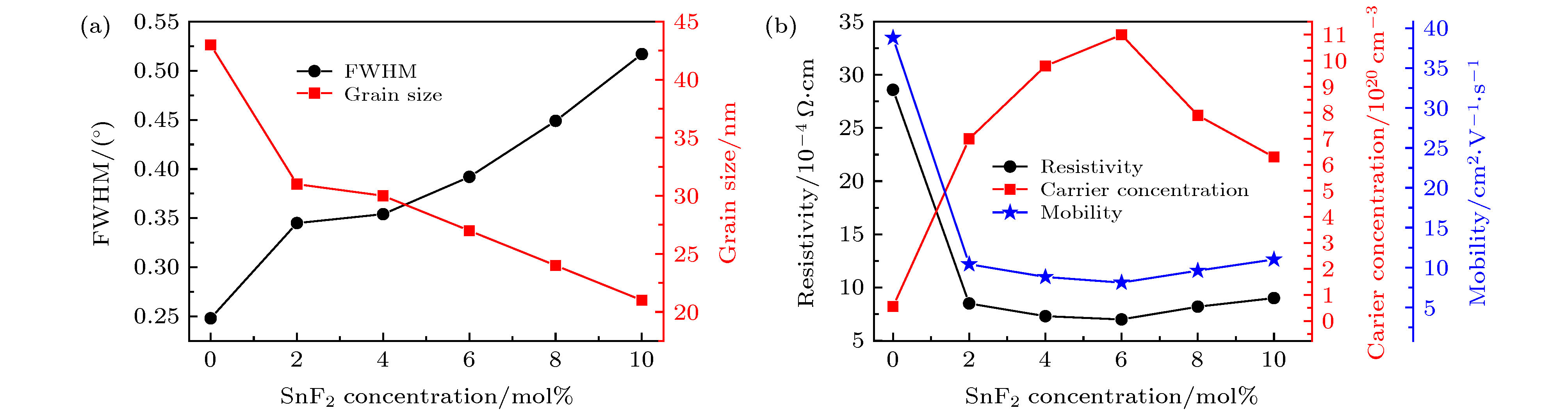
图 7 在不同SnF2浓度下 (a) FTO薄膜 (110) 晶面衍射的半峰宽和晶粒尺寸的变化和 (b) FTO薄膜的电阻率、载流子浓度和迁移率的变化[52]
Fig. 7. (a) Variation of full-width-at-half-maximum and grain size estimated along (1 1 0) diffraction and (b) electrical resistivity, carrier concentration and Hall mobility of the FTO films as a function of SnF2 concentration, 0–10 mol%[52].
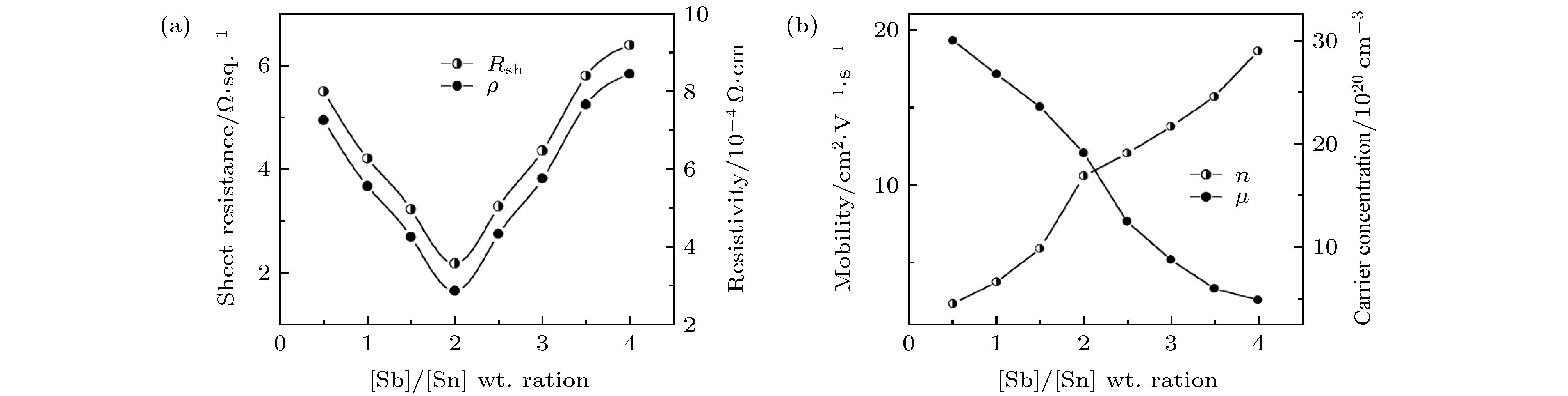
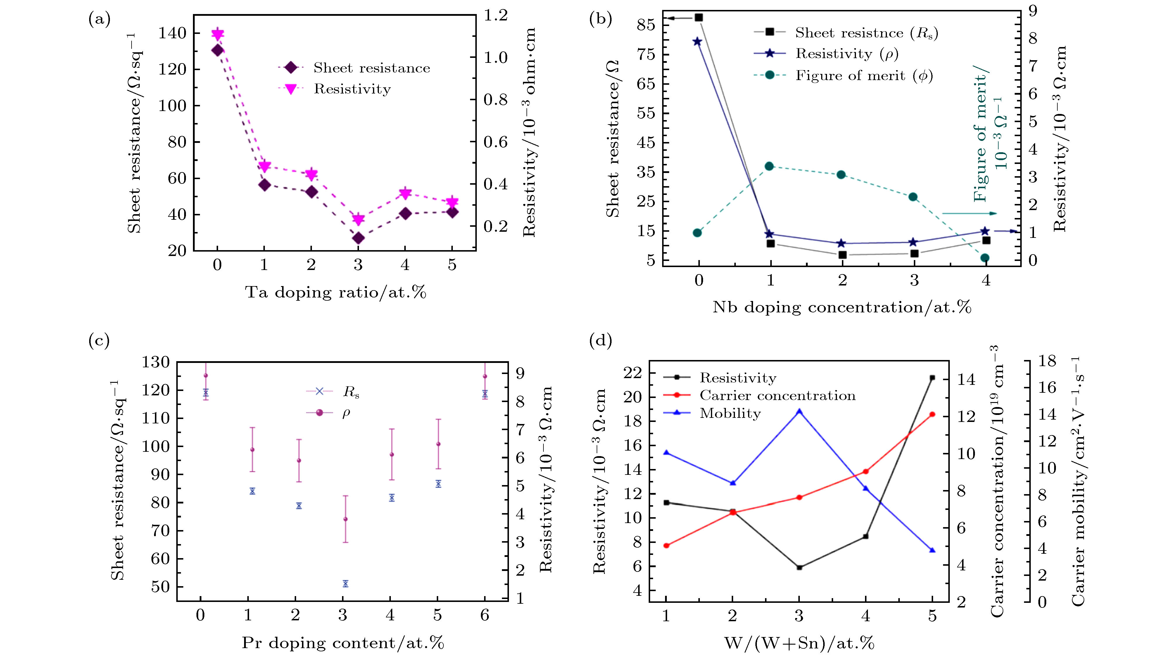
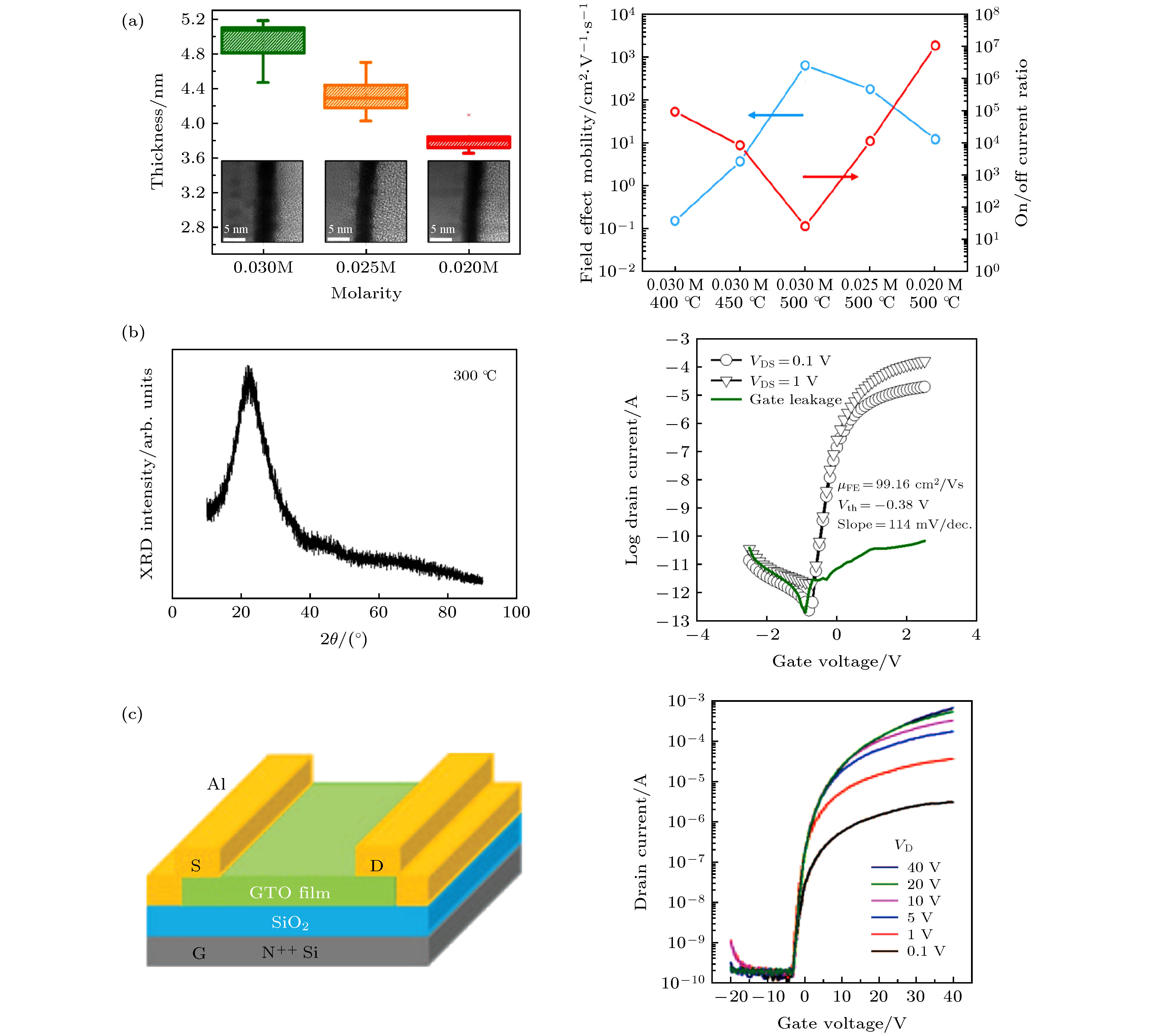
图 10 (a) 不同浓度SnO2薄膜的厚度和电学性能[63]; (b) SnO2薄膜的XRD图谱和TFT的转移特性曲线[64]; (c) Ga掺杂SnO2的TFT示意图及其转移特性曲线[65]
Fig. 10. (a) The thickness and electrical properties of SnO2 films with different concentration[63]; (b) the XRD pattern of SnO2 film and the transfer characteristic curve of SnO2 TFT[64]; (c) the schematic cross-sectional diagram of Ga doped SnO2 TFT and corresponding transfer characteristic curve[65].
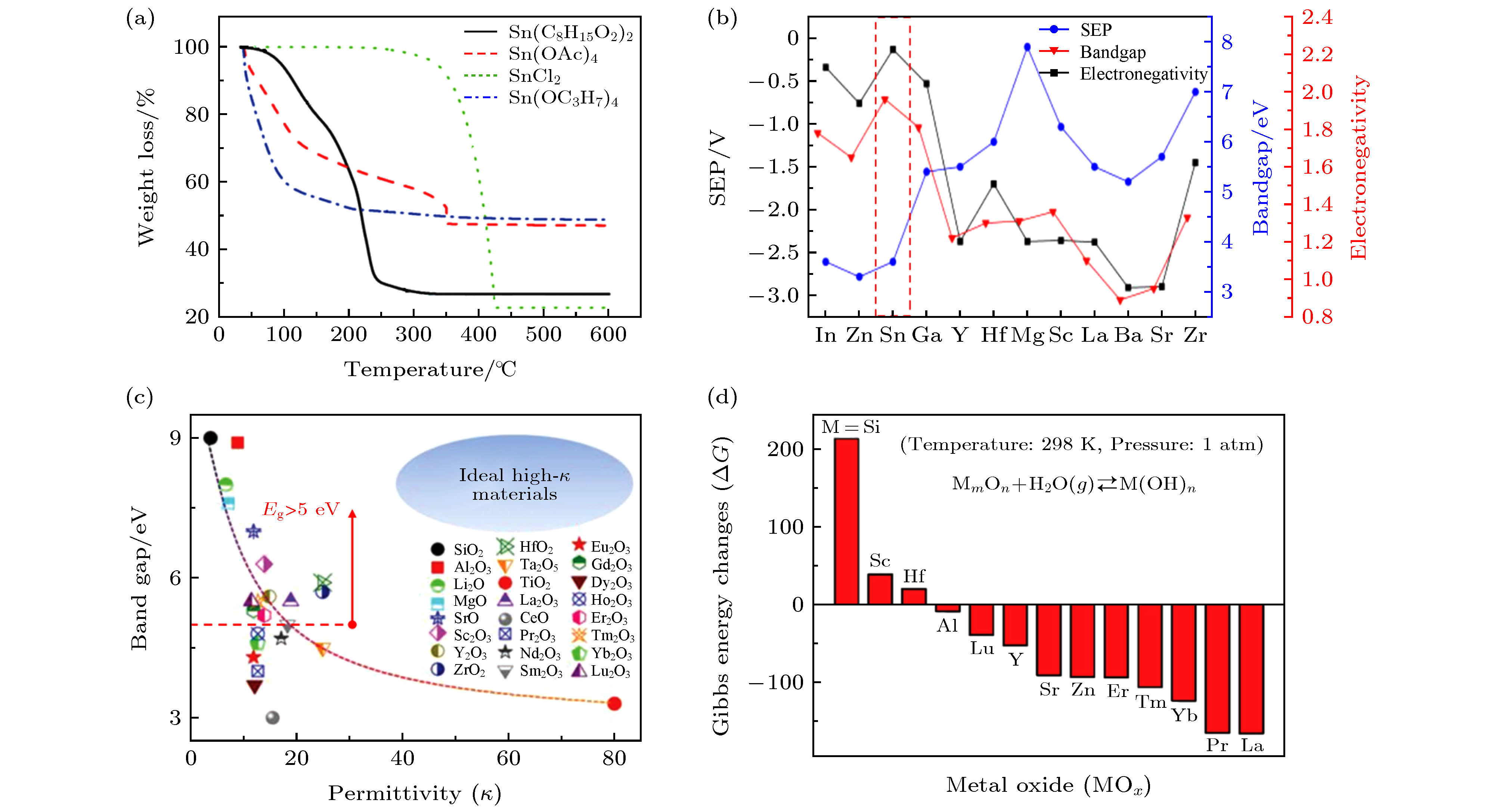
图 11 (a) 不同锡前驱体溶液的热重分析曲线[69]; (b) 不同原子的标准电极电位、带隙和电负性[70]; (c) 不同氧化物介电材料的高介电常数和能带值[71]; (d) 在标准条件下, 高介电常数的氧化物吸湿反应的吉布斯能量变化[71]
Fig. 11. (a) Thermogravimetric analyses curves of various Sn precursors[69]; (b) standard electrode potential, bandgap, and electronegativity of In, Zn, Sn, and carrier suppressible atoms[70]; (c) permittivity and band gap for different oxide dielectrics[71]; (d) Gibbs energy changes for moisture absorption reactions in high permittivity oxides under standard conditions[71].

图 12 不同掺杂浓度SnO2基薄膜的透过率图谱 (a) Ga掺杂SnO2[75]; (b) Co掺杂SnO2[81]; (c) Mn掺杂SnO2[80]; (d) 不同掺杂浓度下Mg掺杂SnO2薄膜的光学吸收图谱[79]
Fig. 12. The transmittance spectra of SnO2-based films with different dopant concentration: (a) Ga doped SnO2[75]; (b) Co doped SnO2[81]; (c) Mn doped SnO2[80]; (d) the optical absorption spectra of Mg-doped SnO2 thin films with different concentration[79].
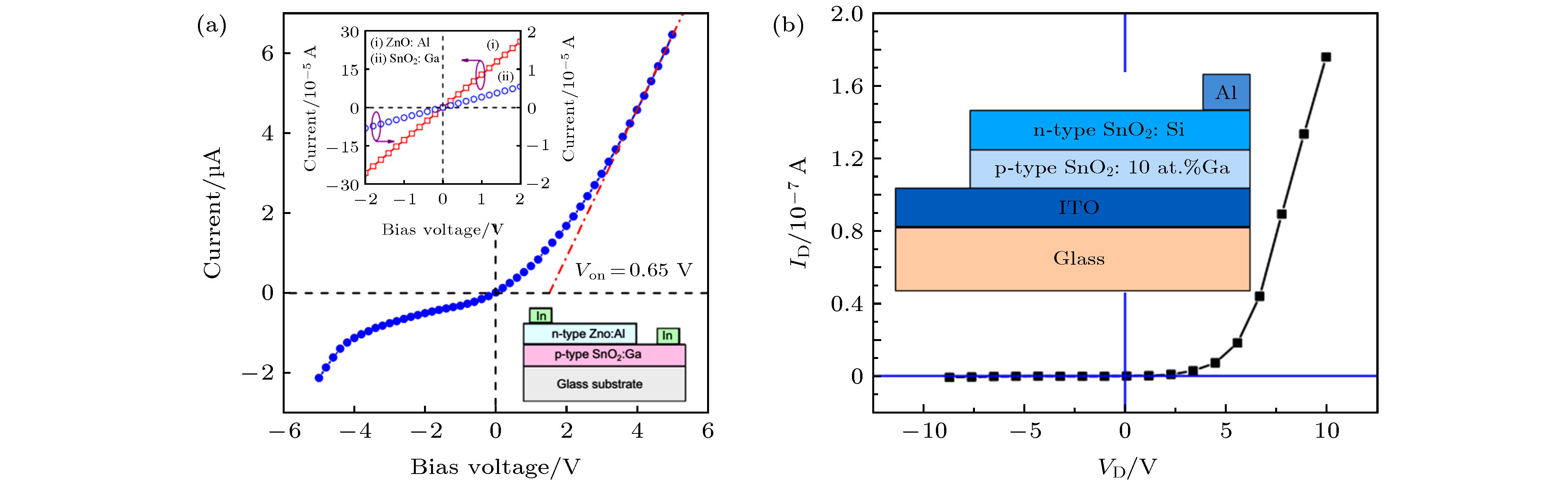
表 1 不同卤素元素的电负性、X—H和X—Sn键解离能和原子半径[31,50]
Table 1. The electronegativity, BDE of X—H and X— Sn, atomic radius for halogen elements[31,50].
Element Electroneg-
ativityBDE of X-H/kJ·mol–1 Atomic radius/nm BDE of X-Sn/kJ·mol–1 F 4.0 569.68 0.42 476 Cl 3.0 431.36 0.79 350 Br 2.8 366.16 1.2 337 BDE: Bond dissociation energy  下载: 导出CSV
表 2 不同元素掺杂SnO2薄膜的电学参数和透过率
Table 2. The electrical parameters and transmittance of SnO2 thin films with different dopants.
Doping elements Conductivity/Ω–1·cm–1 Carrier density /cm–3 Hall Mobility /cm2·V–1·s–1 Transmittance/% Technique Ref. F 0.33 × 10³ 2.62 × 10²⁰ 7.96 86 spray pyrolysis [51] F 1.43 × 10³ 1.10 × 10²¹ 8.1 90 dip-coating [52] Li, F 2.70 × 10³ 5.62 × 10²⁰ 29.1 70 spray pyrolysis [53] P, F 4.0 × 10⁵ 8.30 × 1026 0.0032 86 spray pyrolysis [54] Sb 0.36 × 10³ 6.37 × 10²¹ 0.347 61 spin-coating [55] Sb 3.50 × 10³ 1.68 × 10²¹ 12.03 — spray pyrolysis [56] Ta 0.50 × 10³ 1.30 × 10²⁰ 29.26 80 spray pyrolysis [57] Pr 0.26 × 10³ 8.70 × 10¹⁹ 18.75 80 spray pyrolysis [59] W 0.17 × 10³ 7.60 × 10¹⁹ 14.2 90 dip-coating [60] Nb 0.23 × 10³ 5.00 × 10¹⁹ 25 70 spray pyrolysis [61]
下载: 导出CSV
表 3 溶液法制备SnO2基TFTs的电学性能
Table 3. Electrical properties of solution-processed SnO2-based TFTs.
Solute Dopant Concentration /mol·L–1 Substrate Channel thickness/nm Annealing temperature /℃ Mobility /cm2·V–1·s–1 Ion/Ioff SS/V·dec–1 Ref. SnCl2·2H2O — 0.02 SiO2/Si 3.8 500 11.2 6.8 × 10⁶ 0.78 [63] SnCl2·2H2O — 0.167 HfO2/Mo 9.2 300 99.16 1.7 × 10⁸ 0.114 [64] SnCl2·2H2O Ga(NO3)3
·xH2O0.12 SiO2/Si — 400 4.1 6.6 × 10⁶ 0.77 [65] SnCl2·2H2O — 0.03 SiO2/Si — 500 12.18 5 × 10⁷ 1.17 [66] SnCl2·2H2O — 0.1 ZrO2/ITO 22 400 103 104—105 0.3 [67] C16H30O4Sn — 0.5 Al2O3/ITO 15 350 96.4 2.2 × 10⁶ 0.26 [68]
下载: 导出CSV
表 4 溶液法制备p型SnO2基薄膜的电学性能
Table 4. Electrical properties of solution-processed p type SnO2-based films.
Solute Dopant Resistivity
/Ω·cmCarrier
density/cm–3Hall Mobility
/cm2·V–1·s–1Bandgap/eV Technique Ref. SnCl2·2H2O AlCl3 3.6 × 10⁻² 6.7 × 10¹⁸ 25.90 4.11 spray pyrolysis [74] SnCl2·2H2O Ga(NO3)3·H2O 1.6 1.70 × 10¹⁸ 6.34 3.83 spin-coating [75] SnCl2·2H2O InCl3·4H2O 20.4 1.85 × 10¹⁷ 1.57 3.8 dip-coating [76] SnCl2·2H2O InCl3·4H2O, GaCl3 0.17 9.5 × 10¹⁷ 39.2 3.38 spray pyrolysis [77] SnCl2·2H2O FeCl3·6H2O 660 1.4 × 10¹⁵ 6.75 3.75 dip-coating [78] SnCl2·2H2O MgCl2·6H2O 2.5 × 10⁴ 1014 1.6 3.73 spin-coating [79] SnCl2·2H2O MnCl2 359.1 6.72 × 10¹⁴ 6.14 3.85 dip-coating [80] SnCl2·2H2O CoCl2·6H2O 140 1.47 × 10¹⁵ 8.25 3.81 spin-coating [81]
下载: 导出CSV
-
[1] Grundmann M, Frenzel H, Lajn A, Lorenz M, Schein F, von Wenckstern H 2010 Phys. Status Solidi Appl. Mater. Sci. 207 1437
Google Scholar
[2] Yu X, Marks T J, Facchetti A 2016 Nat. Mater. 15 383
Google Scholar
[3] Park J, Kim H, Kim I 2014 J. Electroceram. 32 117
Google Scholar
[4] Hosono H 2007 Thin Solid Films 515 6000
Google Scholar
[5] Park J S, Maeng W J, Kim H S, Park J S 2012 Thin Solid Films 520 1679
Google Scholar
[6] Facchetti A, Marks T J 2010 Transparent Electron. From Synth. to Appl. 561 2002
[7] Fortunato E, Barquinha P, Martins R 2012 Adv. Mater. 24 2945
Google Scholar
[8] Chopra K L, Major S, Pandya D K 1983 Thin Solid Films. 102 1
Google Scholar
[9] Nomura K, Ohta H, Takagi A, Kamiya T, Hirano M, Hosono H 2004 Nature 432 488
Google Scholar
[10] Yang T, Qin X, Wang H H, Jia Q, Yu R, Wang B, Wang J, Ibrahim K, Jiang X, He Q 2010 Thin Solid Films 518 5542
Google Scholar
[11] Fang F, Zhang Y, Wu X, ShaO Q, Xie Z 2015 Mater. Res. Bull. 68 240
Google Scholar
[12] Ning H L, Liu X Z, Zhang H K, Fang Z Q, Cai W, Chen J Q, Yao R H, Xu M, Wang L, Lan L F, Peng J B, Wang X F, Zhang Z C 2017 Materials (Basel) 10 24
Google Scholar
[13] Jadhav H, Suryawanshi S, More M A, Sinha S 2017 Appl. Surf. Sci. 419 764
Google Scholar
[14] El-Gendy Y A 2017 Phys. B Condens. Matter 526 59
Google Scholar
[15] Bae J Y, Park J, Kim H Y, Kim H S, Park J S 2015 ACS Appl. Mater. Interfaces 7 12074
Google Scholar
[16] Jiménez V M, Espinós J P, González-Elipe A R, Caballero A, Yubero F 1999 J. Phys. IV 9 749
Google Scholar
[17] Choi Y J, Gong S C, Johnson D C, Golledge S, Yeom G Y, Park H H 2013 Appl. Surf. Sci. 269 92
Google Scholar
[18] Park J W, Kang B H, Kim H J 2020 Adv. Funct. Mater. 30 1904632
Google Scholar
[19] Ning H L, Liu X Z, Ruan H G, Peng C, Huang F X, Deng Y X, Yuan W J, Yao R H, Qiu B, Wang X F, Peng J B 2019 AIP Adv. 9 11
Google Scholar
[20] Salmani E, Laghrissi A, Lamouri R, Rouchdi M, Dehmani M, Ez-Zahraouy H, Hassanain N, Mzerd A, Benyoussef A 2018 Opt. Quantum Electron. 50 85
Google Scholar
[21] Pons D, Bourgoin J C 1985 J. Phys. C Solid State Phys. 18 3839
Google Scholar
[22] Shukla T S 2012 J. Sens. Technol. 2 102
Google Scholar
[23] Scanlon D O, Watson G W 2012 J. Mater. Chem. 22 25236
Google Scholar
[24] Terrier C, Chatelon J P, Berjoan R, Roger J A 1995 Thin Solid Films 263 37
Google Scholar
[25] Mäki-Jaskari M A, Rantala T T 2002 Phys. Rev. B - Condens. Matter Mater. Phys. 65 1
Google Scholar
[26] Kılıç Ç, Zunger A 2002 Phys. Rev. Lett. 88 955011
Google Scholar
[27] Singh A K, Janotti A, Scheffler M, van De Walle C G 2008 Phys. Rev. Lett. 101 1
Google Scholar
[28] 倪佳苗, 赵修建, 郑小林, 赵江 2009 真空科学与技术学报 29 531
Google Scholar
NI J M, Zhao X J, Zheng X L, Zhao J 2009 Zhenkong Kexue Yu Jishu Xuebao 29 531
Google Scholar
[29] 望咏林, 颜悦, 沈玫, 贺会权, 张官理 2006 材料导报 20 317
Google Scholar
Wang Y L, Yan Y, Shen M, He H Q, Zhang G L 2006 Mater. Rev. 20 317
Google Scholar
[30] 刘宏燕, 颜悦, 望咏林, 伍建华, 张官理, 厉蕾 2015 航空材料学报 35 63
Liu H Y, Yan Y, Wang Y L, Wu J H, Zhang G L, Li L J. Aeronaut. Mater. 35 63 (in Chinese)
[31] 王立坤, 郁建元, 王丽, 牛孝友, 付晨, 邱茹蒙, 晏伟静, 赵洪力 2018 硅酸盐学报 46 590
Wang L K, Yu J Y, Wang L, Niu X Y, Fu C, Qiu Y M, Yan W J, Zhao H L 2018 J. Chin. Ceram. Soc. 46 590
[32] Noguchi S, Sakata H 1980 J. Phys. D. Appl. Phys. 13 1129
Google Scholar
[33] Galceran Mestres M, Pujol Baiges M C, Aguiló Díaz M 2010 Ph. D. Dissertation (Tarragona: Universitat Rovira i Virgili.)
[34] 武志刚, 高建峰 2010 精细化工 027 21
Wu Z G, Gao J F 2010 Fine Chem. 027 21
[35] Park B, Na S Y, Bae I G 2019 Sci. Rep. 9 1
Google Scholar
[36] Filipovic L, Selberherr S, Mutinati G C, Brunet E, Steinhauer S, Köck A, Teva J, Kraft J, Siegert J, Schrank F 2013 Proc. world. Cong. Eng. 2 987
[37] Aymerich M, Gómez-Varela A I, Álvarez E, Flores-Arias M T 2016 Materials (Basel. 9 728
Google Scholar
[38] Lau G K, Shrestha M 2017 Micromachines 8 1
Google Scholar
[39] Krebs F C 2009 Sol. Energy Mater. Sol. Cells. 93 394
Google Scholar
[40] 李宁, 卢迪芬 2004 玻璃与搪瓷 6 12
Google Scholar
Li N, Lu D F 2004 Glass&Enamel 6 12
Google Scholar
[41] Korotcenkov G, Brinzari V, Schwank J, DiBattista M, Vasiliev A 2001 Sensors Actuators, B Chem. 77 244
Google Scholar
[42] Falcony C, Aguilar-Frutis M A, García-Hipólito M 2018 Micromachines 9 1
Google Scholar
[43] Landau L, Levich B 1988 Dyn. Curved Front. 17 141
[44] Vilà A, Gomez A, Portilla L, Morante J R 2014 Thin Solid Films 553 118
Google Scholar
[45] Betz U, Kharrazi Olsson M, Marthy J, Escolá M F, Atamny F 2006 Surf. Coatings Technol. 200 5751
Google Scholar
[46] Lee S M, Lee J M, Kwon S J, Cho E S 2013 Mol. Cryst. Liq. Cryst. 586 138
Google Scholar
[47] May C, Tomita Y, Toerker M, Eritt M, Loeffler F, Amelung J, Leo K 2008 Thin Solid Films 516 4609
Google Scholar
[48] Park S K, Han J I, Kim W K, Kwak M G 2001 Thin Solid Films 397 49
Google Scholar
[49] Agashe C, Major S S 1996 J. Phys. D. Appl. Phys. 29 2988
Google Scholar
[50] Luo Y R 2007 Comprehensive Handbook of Chemical Bond Energies(Boca Raton: CRC Press) p1
[51] Karthick P, Vijayanarayanan D, Sridharan M, Ananth A K, Sanjeeviraja C, Jeyadheepan K 2017 Thin Solid Films 631 1
Google Scholar
[52] Tran Q P, Fang J S, Chin T S 2015 Mater. Sci. Semicond. Process. 40 664
Google Scholar
[53] Lee K M, Shih K L, Chiang C H, Suryanarayanan V, Wu C G 2014 Thin Solid Films 570 7
Google Scholar
[54] Upadhyay J P, Vishwakarma S R, Prasad H C 1988 Thin Solid Films 167 7
Google Scholar
[55] An H R, Kim C, Oh S T, Ahn H J 2014 Ceram. Int. 40 385
Google Scholar
[56] Elangovan E, Shivashankar S A, Ramamurthi K 2005 J. Cryst. Growth 276 215
Google Scholar
[57] Turgut G 2015 Thin Solid Films 594 56
Google Scholar
[58] Turgut G, Keskenler E F, Aydin S, Sönmez E, Doǧan S, Düzgün B, Ertuǧrul M 2013 Superlattices Microstruct. 56 107
Google Scholar
[59] Turgut G 2015 Philos. Mag. 95 1607
Google Scholar
[60] Huang Y, Li D, Feng J, Li G, Zhang Q 2010 J. Sol-Gel Sci. Technol. 54 276
Google Scholar
[61] Gokulakrishnan V, Parthiban S, Jeganathan K, Ramamurthi K 2011 J. Mater. Sci. 46 5553
Google Scholar
[62] Marius G, Heiko F, Alexander L, Michael L, Friedrich S, H. von W 2010 Phys. Status Solidi A 1449 1437
[63] Jang B, Kim T, Lee S, Lee W Y, Kang H, Cho C S, Jang J 2018 IEEE Electron Device Lett. 39 1179
Google Scholar
[64] Avis C, Ki Y G, Jang J, 2019 Materials (Basel) 12 3341
Google Scholar
[65] Liu C, Wang Z 2018 AM-FPD 2018 - 25 th International Workshop on Active-Matrix Flatpanel Displays Devices Kyoto, Japan July 3−6, 2018 p
[66] Lee W, Jang B, Lee S, Kim T, Jang J 2018 25 th Int. Work. Act. Flatpanel Displays Devices 1
[67] Jang J, Kitsomboonloha R, Swisher S L, Park E S, Kang H, Subramanian V 2013 Adv. Mater. 25 1042
Google Scholar
[68] Huang G, Duan L, Dong G, Zhang D, Qiu Y 2014 ACS Appl. Mater. Interfaces 6 20786
Google Scholar
[69] Zhao Y, Dong G, Duan L, Qiao J, Zhang D, Wang L, Qiu Y 2012 RSC Adv. 2 5307
Google Scholar
[70] Kim S J, Yoon S, Kim H J 2014 Japanese journal of applied physics 2 1
Google Scholar
[71] Liu A, Zhu H, Sun H, Xu Y, Noh Y Y 2018 Adv. Mater. 30 1
Google Scholar
[72] Wang Z, Nayak P K, Caraveo-Frescas J A, Alshareef H N 2016 Adv. Mater. 28 3831
Google Scholar
[73] Hiroshi K, Hiroshi Yanagi K U 2000 MRS Bull. 25 28
Google Scholar
[74] Bagheri-Mohagheghi M M, Shokooh-Saremi M 2004 J. Phys. D. Appl. Phys. 37 1248
Google Scholar
[75] Tsay C Y, Liang S C 2015 J. Alloys Compd. 622 644
Google Scholar
[76] Ji Z, He Z, Song Y, Liu K, Ye Z Z 2003 J. Cryst. Growth 259 282
Google Scholar
[77] Mao Q N, Ji Z G, Zhao L N 2010 Phys. Status Solidi B 247 299
Google Scholar
[78] Soitah T N, Yang C, Sun L 2010 Mater. Sci. Semicond. Process. 13 125
Google Scholar
[79] Li X, Deng R, Li Y, Yao B, Ding Z, Qin J, Liang Q 2016 Ceram. Int. 42 5299
Google Scholar
[80] Ghodsi F E, Mazloom J 2012 Appl. Phys. A Mater. Sci. Process. 108 693
Google Scholar
[81] Mazloom J, Ghodsi F E 2013 Mater. Res. Bull. 48 1468
Google Scholar
[82] Ye Q, Zhang X, Guo D, Xu W, Ning H, Qiu T, Li J, Hou D, Yao R, Peng J 2020 Coatings 10 399
Google Scholar

 下载:
下载:
计量
- 文章访问数: 21871
- PDF下载量: 571
- 被引次数: 0
